Quectel BG96 Manual
Lpwa module
Hide thumbs
Also See for BG96:
- Developer's manual (90 pages) ,
- Hardware design (79 pages) ,
- Application note (53 pages)

Related Manuals for Quectel BG96


Summary of Contents for Quectel BG96
- Page 1 BG96 Hardware Design LPWA Module Series Rev. BG96_Hardware_Design_V1.4 Date: 2019-08-15 Status: Released www.quectel.com...
- Page 2 QUECTEL OFFERS THE INFORMATION AS A SERVICE TO ITS CUSTOMERS. THE INFORMATION PROVIDED IS BASED UPON CUSTOMERS’ REQUIREMENTS. QUECTEL MAKES EVERY EFFORT TO ENSURE THE QUALITY OF THE INFORMATION IT MAKES AVAILABLE. QUECTEL DOES NOT MAKE ANY WARRANTY AS TO THE INFORMATION CONTAINED HEREIN, AND DOES NOT ACCEPT ANY LIABILITY FOR ANY INJURY, LOSS OR DAMAGE OF ANY KIND INCURRED BY USE OF OR RELIANCE UPON THE INFORMATION.
-
Page 3: About The Document
LPWA Module Series BG96 Hardware Design About the Document History Revision Date Author Description Lyndon LIU/ 2017-08-04 Initial Daryl DU 1. Modified GSM features in Table 2. 2. Added a note for e-I-DRX in Chapter 3.3. 2017-08-31 Daryl DU 3. Elaborated the description of e-I-DRX in Chapter 3.4.3. - Page 4 Table 22. 10. Updated the GPIO configuration command in Chapter 3.17. 11. Updated BG96 operating frequency in Table 27. 12. Updated GNSS frequency in Table 29. 13. Updated BG96 current consumption in Table 34. 14. Updated the recommended stencil thickness and the peak reflow temperature in Chapter 8.2.
-
Page 5: Table Of Contents
LPWA Module Series BG96 Hardware Design Contents About the Document ........................... 2 Contents ............................... 4 Table Index ..............................6 Figure Index ..............................8 Introduction ............................9 1.1. Safety Information ........................10 Product Concept ..........................11 2.1. General Description ........................11 2.2. - Page 6 LPWA Module Series BG96 Hardware Design 3.17. GPIO Interfaces ........................46 GNSS Receiver ........................... 47 4.1. General Description ........................47 4.2. GNSS Performance ........................47 4.3. Layout Guidelines ........................48 Antenna Interfaces ..........................49 5.1. Main Antenna Interface ......................49 5.1.1.
- Page 7 LPWA Module Series BG96 Hardware Design Table Index TABLE 1: FREQUENCY BANDS OF BG96 MODULE ..................11 TABLE 2: KEY FEATURES OF BG96 MODULE ....................12 TABLE 3: DEFINITION OF I/O PARAMETERS ....................18 TABLE 4: PIN DESCRIPTION ........................... 18 TABLE 5: OVERVIEW OF OPERATING MODES .....................
- Page 8 LPWA Module Series BG96 Hardware Design TABLE 42: TERMS AND ABBREVIATIONS ...................... 73 TABLE 43: DESCRIPTION OF DIFFERENT CODING SCHEMES ..............76 TABLE 44: GPRS MULTI-SLOT CLASSES ...................... 77 TABLE 45: EDGE MODULATION AND CODING SCHEMES ................79 BG96_Hardware_Design 7 / 79...
- Page 9 LPWA Module Series BG96 Hardware Design Figure Index FIGURE 1: FUNCTIONAL DIAGRAM ....................... 14 FIGURE 2: PIN ASSIGNMENT (TOP VIEW)..................... 17 FIGURE 3: SLEEP MODE APPLICATION VIA UART ..................27 FIGURE 4: POWER SUPPLY LIMITS DURING BURST TRANSMISSION ............29 FIGURE 5: STAR STRUCTURE OF THE POWER SUPPLY................
-
Page 10: Introduction
This document helps customers quickly understand the interface specifications, electrical and mechanical details, as well as other related information of BG96. To facilitate application designs, it also includes some reference designs for customers’ reference. The document, coupled with application notes and user guides, can help customers use the module to design and set up mobile applications easily. -
Page 11: Safety Information
BG96. Manufacturers of the cellular terminal should send the following safety information to users and operating personnel, and incorporate these guidelines into all manuals supplied with the product. If not so, Quectel assumes no liability for customers’ failure to comply with these precautions. -
Page 12: Product Concept
LTE-FDD B25 is supported on BG96 of R1.2 hardware version. “*” means under development. With a compact profile of 26.5mm × 22.5mm × 2.3mm, BG96 can meet almost all requirements for M2M applications such as smart metering, tracking system, security, wireless POS, etc. -
Page 13: Key Features
LPWA Module Series BG96 Hardware Design 2.2. Key Features The following table describes the detailed features of BG96 module. Table 2: Key Features of BG96 Module Features Details Supply voltage: 3.3V~4.3V Power Supply Typical supply voltage: 3.8V Class 3 (23dBm± 2dB) for LTE-FDD bands Class 3 (23dBm±... - Page 14 Used for outputting GNSS data or NMEA sentences 115200bps baud rate 3GPP TS 27.007 and 3GPP TS 27.005 AT commands, as well as Quectel AT Commands enhanced AT commands Network Indication One NETLIGHT pin for network connectivity status indication...
-
Page 15: Functional Diagram
When the temperature returns to the normal operating temperature levels, the module will meet 3GPP specifications again. 2.3. Functional Diagram The following figure shows a block diagram of BG96 and illustrates the major functional parts. Power management ... -
Page 16: Evaluation Board
BG96 Hardware Design 2.4. Evaluation Board In order to help customers develop applications conveniently with BG96, Quectel supplies the evaluation board (EVB), USB to RS-232 converter cable, USB data cable, earphone, antenna and other peripherals to control or test the module. For more details, please refer to document [1]. -
Page 17: Application Interfaces
LPWA Module Series BG96 Hardware Design Application Interfaces BG96 is equipped with 102 LGA pads that can be connected to customers’ cellular application platforms. The following sub-chapters will provide detailed description of interfaces listed below: Power supply (U)SIM interface ... -
Page 18: Pin Assignment
LPWA Module Series BG96 Hardware Design 3.1. Pin Assignment The following figure shows the pin assignment of BG96. PSM_IND ANT_GNSS ADC1 USIM_GND PCM_CLK USIM_CLK PCM_SYNC USIM_DATA PCM_IN USIM_RST PCM_OUT USIM_VDD GPIO64 USIM_PRESENCE USB_VBUS USB_DP I2C_SDA I2C_SCL USB_DM USB_BOOT RESERVED RESERVED... -
Page 19: Pin Description
GND pads should be connected to ground in the design. PWRKEY output voltage is 0.8V because of the diode drop in the Qualcomm chipset. 3.2. Pin Description The following tables show the pin definition and description of BG96. Table 3: Definition of I/O Parameters Type... - Page 20 LPWA Module Series BG96 Hardware Design module’s RF Vnorm=3.8V part Power supply for external GPIO’s Provide 1.8V Vnorm=1.8V VDD_EXT for external pull-up circuits. max=50mA circuit If unused, keep this pin open. 3, 31, 48, 50, 54, 55, 58, 59, 61,...
- Page 21 LPWA Module Series BG96 Hardware Design specification. Compliant with USB USB differential Require differential USB_DM 2.0 standard data bus (-) impedance of 90Ω. specification. (U)SIM Interface Pin Name Pin No. Description DC Characteristics Comment min=-0.3V (U)SIM card 1.8V power domain.
- Page 22 LPWA Module Series BG96 Hardware Design max=0.45V min=2.55V Specified USIM_GND ground for (U)SIM card UART1 Interface Pin Name Pin No. Description DC Characteristics Comment min=-0.3V Data terminal 1.8V power domain. max=0.6V ready (sleep If unused, keep this min=1.2V mode control) pin open.
- Page 23 LPWA Module Series BG96 Hardware Design UART3 Interface Pin Name Pin No. Description DC Characteristics Comment 1.8V power domain. max=0.45V UART3_TXD Transmit data If unused, keep this min=1.35V pin open. min=-0.3V 1.8V power domain. max=0.6V UART3_RXD Receive data If unused, keep this min=1.2V...
- Page 24 LPWA Module Series BG96 Hardware Design Main antenna ANT_MAIN 50Ω impedance. interface 50Ω impedance. GNSS antenna ANT_GNSS If unused, keep this interface pin open. Other Interface Pins Pin Name Pin No. Description DC Characteristics Comment 1.8V power domain. Power saving max=0.45V...
-
Page 25: Operating Modes
LPWA Module Series BG96 Hardware Design General purpose analog Voltage range: If unused, keep this ADC1 to digital 0.3V to 1.8V pin open. converter interface General purpose analog Voltage range: If unused, keep this ADC0 to digital 0.3V to 1.8V pin open. -
Page 26: Power Saving
During this mode, the module can still receive paging message, SMS and TCP/UDP data from the network normally. Power Saving BG96 module may enter Power Saving Mode for reducing its power consumption. PSM Mode is similar to power-off, but the module remains registered on the network and there is no (PSM) need to re-attach or re-establish PDN connections. -
Page 27: Power Saving Mode (Psm)
The execution of AT+CFUN command will not affect GNSS function. 3.4.2. Power Saving Mode (PSM) BG96 module can enter PSM for reducing its power consumption. The mode is similar to power-off, but the module remains registered on the network and there is no need to re-attach or re-establish PDN connections. -
Page 28: Sleep Mode
Please refer to document [2] for details about AT+CEDRXS command. 3.4.4. Sleep Mode BG96 is able to reduce its current consumption to a lower value during the sleep mode. The following sub-chapters describe the power saving procedure of BG96 module. -
Page 29: Power Supply
Driving the host DTR to low level will wake up the module. When BG96 has URC to report, RI signal will wake up the host. Please refer to Chapter 3.14 for details about RI behavior. AP_READY will detect the sleep state of the host (can be configured to high level or low level detection). -
Page 30: Monitor The Power Supply
LPWA Module Series BG96 Hardware Design Burst Burst Transmission Transmission VBAT Ripple Drop Min.3.3V Figure 4: Power Supply Limits during Burst Transmission To decrease voltage drop, a bypass capacitor of about 100µF with low ESR should be used, and a multi-layer ceramic chip capacitor (MLCC) array should also be reserved due to its low ESR. -
Page 31: Turn On And Off Scenarios
Qualcomm chipset. When BG96 is in power off mode, it can be turned on by driving the PWRKEY pin to a low level for at least 500ms. It is recommended to use an open drain/collector driver to control the PWRKEY. After STATUS pin outputs a high voltage level, PWRKEY pin can be released. - Page 32 LPWA Module Series BG96 Hardware Design PWRKEY Close to S1 Figure 7: Turn on the Module Using Keystroke The power on scenario is illustrated in the following figure. NOTE VBA T ≥500ms ≤0.5V PWRKEY RESET_N ≥ 4.8s STATUS (DO) ≥ 4.2s...
-
Page 33: Turn Off Module
LPWA Module Series BG96 Hardware Design 3.6.2. Turn off Module Either of the following methods can be used to turn off the module: Normal power down procedure: Turn off the module using the PWRKEY pin. Normal power down procedure: Turn off the module using AT+QPOWD command. - Page 34 LPWA Module Series BG96 Hardware Design Table 8: RESET_N Pin Description Pin Name Pin No. Description DC Characteristics Comment Vnorm=1.8V RESET_N Reset the module max=0.5V The recommended circuit is similar to the PWRKEY control circuit. An open drain/collector driver or button can be used to control the RESET_N.
-
Page 35: U)Sim Interface
LPWA Module Series BG96 Hardware Design The reset scenario is illustrated in the following figure. VBA T ≤460ms ≥150ms RESET_N ≤0.5V Module Running Resetting Restart Status Figure 12: Timing of Resetting Module NOTES Use RESET_N only when turning off the module by AT+QPOWD command and PWRKEY pin both failed. - Page 36 LPWA Module Series BG96 Hardware Design BG96 supports (U)SIM card hot-plug via the USIM_PRESENCE pin which supports low level and high level detections. The function is disabled by default. Please refer to document [2] about AT+QSIMDET command for details. The following figure shows a reference design of (U)SIM interface with an 8-pin (U)SIM card connector.
-
Page 37: Usb Interface
(U)SIM card connector. 3.9. USB Interface BG96 contains one integrated Universal Serial Bus (USB) interface which complies with the USB 2.0 specification and supports high-speed (480Mbps) and full-speed (12Mbps) modes. The USB interface is used for AT command communication, data transmission, software debugging and firmware upgrade. - Page 38 Pay attention to the influence of junction capacitance of ESD protection devices on USB data lines. Typically, the capacitance value should be less than 2pF. Keep the ESD protection devices as close to the USB connector as possible. NOTE BG96 module can only be used as a slave device. BG96_Hardware_Design 37 / 79...
-
Page 39: Uart Interfaces
LPWA Module Series BG96 Hardware Design 3.10. UART Interfaces The module provides three UART interfaces: UART1, UART2 and UART3 interfaces. The following are their features. UART1 interface supports 9600bps, 19200bps, 38400bps, 57600bps, 115200bps, 230400bps, 460800bps and 921600bps baud rates, and the default is 115200bps. It is used for data transmission and AT command communication. - Page 40 LPWA Module Series BG96 Hardware Design Table 12: Pin Definition of UART2 Interface Pin Name Pin No. Description Comment DBG_RXD Receive data 1.8V power domain DBG_TXD Transmit data 1.8V power domain Table 13: Pin Definition of UART3 Interface Pin Name Pin No.
- Page 41 LPWA Module Series BG96 Hardware Design VDD_EXT VCCA VCCB VDD_MCU 0.1uF 0.1uF 120K RI_MCU DCD_MCU Translator CTS_MCU RTS_MCU DTR_MCU TXD_MCU RXD_MCU Figure 16: Reference Circuit with Translator Chip Please visit http://www.ti.com for more information. Another example with transistor translation circuit is shown as below. For the design of circuits in dotted lines, please refer to that of circuits in solid lines, but please pay attention to the direction of connection.
-
Page 42: Pcm And I2C Interfaces
BG96 Hardware Design 3.11. PCM and I2C Interfaces* BG96 provides one Pulse Code Modulation (PCM) digital interface and one I2C interface. The following table shows the pin definition of the two interfaces which can be applied on audio codec design. -
Page 43: Network Status Indication
BG96 Hardware Design 3.12. Network Status Indication BG96 provides one network status indication pin: NETLIGHT. The pin is used to drive a network status indication LED. The following tables describe the pin definition and logic level changes of NETLIGHT in different network activity status. -
Page 44: Status
LPWA Module Series BG96 Hardware Design 3.13. STATUS The STATUS pin is used to indicate the operation status of BG96 module. It will output high level when the module is powered on. The following table describes the pin definition of STATUS. -
Page 45: Usb_Boot Interface
The default RI behaviors can be configured flexibly by AT+QCFG=“urc/ri/ring” command. For more details, please refer to document [2]. 3.15. USB_BOOT Interface BG96 provides a USB_BOOT pin. During development or factory production, USB_BOOT can force the module to boot from USB port for firmware upgrade. Table 20: Pin Definition of USB_BOOT Interface Pin Name Pin No. -
Page 46: Adc Interfaces
LPWA Module Series BG96 Hardware Design NOTE It is recommended to reserve the above circuit design during application design. 3.16. ADC Interfaces The module provides two analog-to-digital converter (ADC) interfaces. AT+QADC=0 command can be used to read the voltage value on ADC0 pin. AT+QADC=1 command can be used to read the voltage value on ADC1 pin. -
Page 47: Gpio Interfaces
LPWA Module Series BG96 Hardware Design NOTES ADC input voltage must not exceed 1.8V. It is prohibited to supply any voltage to ADC pins when VBAT is removed. It is recommended to use resistor divider circuit for ADC application, and the divider resistor accuracy should be no less than 1%. -
Page 48: Gnss Receiver
The module supports standard NMEA-0183 protocol, and outputs NMEA sentences at 1Hz data update rate via USB interface by default. By default, BG96 GNSS engine is switched off. It has to be switched on via AT command. For more details about GNSS engine technology and configurations, please refer to document [3]. -
Page 49: Layout Guidelines
LPWA Module Series BG96 Hardware Design Autonomous Hot start @open sky XTRA enabled 1.82 Accuracy Autonomous CEP-50 < 2.5 (GNSS) @open sky NOTES Tracking sensitivity: the lowest GNSS signal value at the antenna port on which the module can keep on positioning for 3 minutes. -
Page 50: Antenna Interfaces
LPWA Module Series BG96 Hardware Design Antenna Interfaces BG96 includes a main antenna interface and a GNSS antenna interface. The antenna ports have an impedance of 50Ω. 5.1. Main Antenna Interface 5.1.1. Pin Definition The pin definition of main antenna interface is shown below. -
Page 51: Reference Design Of Rf Antenna Interface
1880~1920 1880~1920 NOTES LTE-FDD B25 is supported on BG96 of R1.2 hardware version. “*” means under development. 5.1.3. Reference Design of RF Antenna Interface A reference design of main antenna pad is shown as below. A π-type matching circuit should be reserved for better RF performance, and the π-type... -
Page 52: Reference Design Of Rf Layout
LPWA Module Series BG96 Hardware Design 5.1.4. Reference Design of RF Layout For user’s PCB, the characteristic impedance of all RF traces should be controlled to 50Ω. The impedance of the RF traces is usually determined by the trace width (W), the materials’ dielectric constant,... -
Page 53: Gnss Antenna Interface
LPWA Module Series BG96 Hardware Design Figure 26: Coplanar Waveguide Design on a 4-layer PCB (Layer 4 as Reference Ground) In order to ensure RF performance and reliability, the following principles should be complied with in RF layout design: ... -
Page 54: Antenna Installation
LPWA Module Series BG96 Hardware Design Table 29: GNSS Frequency Type Frequency Unit 1575.42± 1.023 GLONASS 1597.5~1605.8 Galileo 1575.42± 2.046 BeiDou 1561.098± 2.046 QZSS 1575.42 A reference design of GNSS antenna interface is shown as below. 0.1uF GNSS Antenna Module... -
Page 55: Recommended Rf Connector For Antenna Installation
LPWA Module Series BG96 Hardware Design Table 30: Antenna Requirements Antenna Type Requirements Frequency range: 1559MHz ~1609MHz Polarization: RHCP or linear VSWR: < 2 (Typ.) GNSS Passive antenna gain: > 0dBi Active antenna noise figure: < 1.5dB Active antenna gain: > 0dBi Active antenna embedded LNA gain: <... - Page 56 LPWA Module Series BG96 Hardware Design Figure 28: Dimensions of the U.FL-R-SMT Connector (Unit: mm) U.FL-LP serial connectors listed in the following figure can be used to match the U.FL-R-SMT. Figure 29: Mechanicals of U.FL-LP Connectors BG96_Hardware_Design 55 / 79...
- Page 57 LPWA Module Series BG96 Hardware Design The following figure describes the space factor of mated connector. Figure 30: Space Factor of Mated Connector (Unit: mm) For more details, please visit http://www.hirose.com. BG96_Hardware_Design 56 / 79...
-
Page 58: Electrical, Reliability And Radio Characteristics
LPWA Module Series BG96 Hardware Design Electrical, Reliability and Radio Characteristics 6.1. Absolute Maximum Ratings Absolute maximum ratings for power supply and voltage on digital and analog pins of the module are listed in the following table. Table 31: Absolute Maximum Ratings Parameter Min. -
Page 59: Operation And Storage Temperatures
When the temperature returns to the normal operating temperature levels, the module will meet 3GPP specifications again. 6.4. Current Consumption The following table shows current consumption of BG96 module. Table 34: BG96 Current Consumption Parameter... - Page 60 LPWA Module Series BG96 Hardware Design Rock Bottom AT+CFUN=0 @Sleep State Sleep DRX=1.28s @ Instrument DRX=1.28s @ Instrument 1.96 Sleep State e-I-DRX=20.48s @ Instrument e-I-DRX=20.48s @ Instrument @Real 2G Network DRX=1.28s @ Instrument DRX=1.28s @ Instrument Idle State e-I-DRX=20.48s @ Instrument e-I-DRX=20.48s @ Instrument...
- Page 61 LPWA Module Series BG96 Hardware Design LTE-TDD B39 @TBD LTE-FDD B1 @22.8dBm LTE-FDD B2 @22.6dBm LTE-FDD B3 @22.6dBm LTE-FDD B4 @22.6dBm LTE-FDD B5 @22.9dBm LTE-FDD B8 @22.7dBm LTE Cat NB1 LTE-FDD B12 @23dBm Data Transfer LTE-FDD B13 @22.9dBm (GNSS OFF) LTE-FDD B18 @23.1dBm...
- Page 62 LPWA Module Series BG96 Hardware Design DCS1800 2UL 3DL @30.1dBm DCS1800 1UL4DL @30.34dBm PCS1900 4UL 1DL @29.64dBm PCS1900 3UL 2DL @29.86dBm PCS1900 2UL 3DL @29.7dBm PCS1900 1UL 4DL @29.94dBm GSM850 4UL1DL @26.02dBm GSM850 3UL 2DL @26.11dBm GSM850 2UL 3DL @26.57dBm GSM850 1UL 4DL @26.92dBm...
-
Page 63: Rf Output Power
Sleep state with UART connected and USB disconnected. The module can enter sleep mode through executing AT+QSCLK=1 command via UART interface and then controlling the module’s DTR pin. For details, please refer to Chapter 3.4.4. 4. LTE-FDD B25 is supported on BG96 of R1.2 hardware version. Table 35: GNSS Current Consumption Description Conditions Typ. -
Page 64: Rf Receiving Sensitivity
LPWA Module Series BG96 Hardware Design DCS1800/PCS1900 (8-PSK) 26dBm± 3dB 0dBm± 5dB 6.6. RF Receiving Sensitivity The following table shows the conducted RF receiving sensitivity of BG96 module. Table 37: BG96 Conducted RF Receiving Sensitivity Sensitivity (dBm) Network Band Primary Diversity... -
Page 65: Electrostatic Discharge
ESD handling precautions that typically apply to ESD sensitive components. Proper ESD handling and packaging procedures must be applied throughout the processing, handling and operation of any application that incorporates the module. The following table shows the electrostatic discharge characteristics of BG96 module. Table 38: Electrostatic Discharge Characteristics Tested Interfaces... -
Page 66: Mechanical Dimensions
LPWA Module Series BG96 Hardware Design Mechanical Dimensions This chapter describes the mechanical dimensions of the module. All dimensions are measured in mm, and the dimensional tolerances are ± 0.05mm unless otherwise specified. 7.1. Mechanical Dimensions of the Module 22.50± 0.15 2.3±... - Page 67 LPWA Module Series BG96 Hardware Design Figure 32: Module Bottom Dimensions (Bottom View) BG96_Hardware_Design 66 / 79...
-
Page 68: Recommended Footprint
LPWA Module Series BG96 Hardware Design 7.2. Recommended Footprint Figure 33: Recommended Footprint (Top View) NOTES For easy maintenance of the module, please keep about 3mm between the module and other components on the host PCB. All reserved pins must be kept open. -
Page 69: Top/Bottom View Of The Module
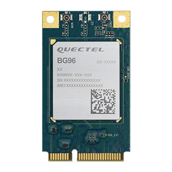
7.3. Top/Bottom View of the Module Figure 34: Top View of the Module Figure 35: Bottom View of the Module NOTE These are renderings of BG96 module. For authentic appearance, please refer to the module that you receive from Quectel. BG96_Hardware_Design 68 / 79... -
Page 70: Storage, Manufacturing And Packaging
Packaging 8.1. Storage BG96 is stored in a vacuum-sealed bag. It is rated at MSL 3, and its storage restrictions are listed below. 1. Shelf life in the vacuum-sealed bag: 12 months at <40º C/90%RH. 2. After the vacuum-sealed bag is opened, devices that will be subjected to reflow soldering or other high temperature processes must be: ... -
Page 71: Manufacturing And Soldering
LPWA Module Series BG96 Hardware Design 8.2. Manufacturing and Soldering Push the squeegee to apply the solder paste on the surface of stencil, thus making the paste fill the stencil openings and then penetrate to the PCB. The force on the squeegee should be adjusted properly so as to produce a clean stencil surface on a single pass. -
Page 72: Packaging
Max reflow cycle 8.3. Packaging BG96 is packaged in a vacuum-sealed bag which is ESD protected. The bag should not be opened until the devices are ready to be soldered onto the application. The reel is 330mm in diameter and each reel contains 250 modules. The following figures show the packaging details, measured in mm. - Page 73 LPWA Module Series BG96 Hardware Design 48.5 Cover tape Direction of feed +0.20 44.5 -0.00 Figure 38: Reel Dimensions Table 40: Reel Packaging Model Name MOQ for MP Minimum Package: 250pcs Minimum Package x 4=1000pcs Size: 370mm × 350mm × 56mm Size: 380mm ×...
-
Page 74: Appendix A References
Table 41: Related Documents Document Name Remark Quectel_UMTS<E_EVB_User_Guide UMTS<E EVB User Guide Quectel_BG96_AT_Commands_Manual BG96 AT Commands Manual Quectel_BG96_GNSS_AT_Commands_Manual BG96 GNSS AT Commands Manual Quectel_RF_Layout_Application_Note RF Layout Application Note Quectel_Module_Secondary_SMT_User_Guide Module Secondary SMT User Guide Table 42: Terms and Abbreviations Abbreviation Description... - Page 75 LPWA Module Series BG96 Hardware Design Electrostatic Discharge Frequency Division Duplex Full Rate GMSK Gaussian Minimum Shift Keying Global System for Mobile Communications Home Subscriber Server Input/Output Inorm Normal Current Light Emitting Diode Low Noise Amplifier Long Term Evolution Mobile Originated...
- Page 76 LPWA Module Series BG96 Hardware Design Transmitting Direction Uplink User Equipment Unsolicited Result Code (U)SIM (Universal) Subscriber Identity Module Vmax Maximum Voltage Value Vnorm Normal Voltage Value Vmin Minimum Voltage Value Maximum Input High Level Voltage Value Minimum Input High Level Voltage Value...
-
Page 77: Appendix B Gprs Coding Schemes
LPWA Module Series BG96 Hardware Design Appendix B GPRS Coding Schemes Table 43: Description of Different Coding Schemes CS-1 CS-2 CS-3 CS-4 Scheme Code Rate Pre-coded USF Radio Block excl.USF and BCS Tail Coded Bits Punctured Bits Data Rate Kb/s 9.05... -
Page 78: Appendix C Gprs Multi-Slot Classes
LPWA Module Series BG96 Hardware Design Appendix C GPRS Multi-slot Classes Twenty-nine classes of GPRS multi-slot modes are defined for MS in GPRS specification. Multi-slot classes are product dependent, and determine the maximum achievable data rates in both the uplink and downlink directions. - Page 79 LPWA Module Series BG96 Hardware Design BG96_Hardware_Design 78 / 79...
-
Page 80: Appendix D Edge Modulation And Coding Schemes
LPWA Module Series BG96 Hardware Design Appendix D EDGE Modulation and Coding Schemes Table 45: EDGE Modulation and Coding Schemes Coding Modulation Coding Family 1 Timeslot 2 Timeslot 4 Timeslot Schemes CS-1: GMSK 9.05kbps 18.1kbps 36.2kbps CS-2: GMSK 13.4kbps 26.8kbps 53.6kbps...
Need help?
Do you have a question about the BG96 and is the answer not in the manual?
Questions and answers