Sign In
Upload
Manuals
Brands
Alinx Manuals
Motherboard
KINTEX-7 FPGA
User Manuals: Alinx KINTEX-7 FPGA Development Board
Manuals and User Guides for Alinx KINTEX-7 FPGA Development Board. We have
3
Alinx KINTEX-7 FPGA Development Board manuals available for free PDF download: User Manual
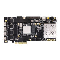
Alinx KINTEX-7 FPGA User Manual (54 pages)
Brand:
Alinx
| Category:
Motherboard
| Size: 2 MB
Table of Contents
Version Record
2
Table of Contents
3
Part 1: FPGA Development Board Introduction
6
Part 2: AC7K325 Core Board
9
Part 2.1: AC7K325 Core Board Introduction
9
Part 2.2: FPGA Chip
10
Part 2.3:DDR3 DRAM
11
Part 2.4: QSPI Flash
15
Part 2.5: Clock Configuration
17
Part 2.5.1: 200Mhz System Clock Source
17
Part 2.5.2: GTX Reference Clock
18
Part 2.6: LED Light
19
Part 2.7: Power Supply
20
Part 2.8: Size Dimension
23
Part 2.9: Board-To-Board Pin Definition
23
Part 3: Carrier Board
32
Part 3.1: Carrier Board Introduction
32
Part 3.2: SFP Interface
32
Part 3.3.: Pcie Card Slot
34
Part 3.4: HDMI Video Output Interface
36
Part 3.5: HDMI Input Interface
41
Part 3.6: SATA Interface
46
Part 3.7: USB to Serial Port
47
Part 3.8: SD Card Slot
48
Part 3.9: 40-Pin Expansion Port
49
Part 3.10: Keys and Leds
50
Part 3.11: JTAG Debug Port
52
Part 3.12: Power Supply
52
Advertisement
Alinx KINTEX-7 FPGA User Manual (45 pages)
Brand:
Alinx
| Category:
Motherboard
| Size: 2 MB
Table of Contents
Version Record
2
Table of Contents
3
Part 1: FPGA Development Board Introduction
5
Part 2: AC7K325 Core Board
8
Part 2.1: AC7K325 Core Board Introduction
8
Part 2.2: FPGA Chip
9
Part 2.3:DDR3 DRAM
10
Part 2.4: QSPI Flash
14
Part 2.5: Clock Configuration
16
Part 2.5.1: 200Mhz System Clock Source
16
Part 2.5.2: GTX Reference Clock
17
Part 2.6: LED Light
18
Part 2.7: Power Supply
19
Part 2.8: Size Dimension
22
Part 2.9: Board-To-Board Pin Definition
22
Part 3: Carrier Board
31
Part 3.1: Carrier Board Introduction
31
Part 3.2: SFP Interface
31
Part 3.3.: Pcie Card Slot
33
Part 3.4: SDI Output Interface
35
Part 3.5: SDI Input Interface
37
Part 3.6: USB to Serial Port
38
Part 3.7: SD Card Slot
38
Part 3.9: 40-Pin Expansion Port
39
Part 3.9: Keys and Leds
41
Part 3.10: JTAG Debug Port
43
Part 3.11: Power Supply
43
Part 3.12: Size Dimension
45
Alinx KINTEX-7 FPGA User Manual (41 pages)
Brand:
Alinx
| Category:
Motherboard
| Size: 1 MB
Table of Contents
Version Record
2
Table of Contents
3
Part 1: FPGA Development Board Introduction
5
Part 2: AC7K325B Core Board
8
Part 2.1: AC7K325 Core Board Introduction
8
Part 2.2: FPGA Chip
9
Part 2.3: DDR3 DRAM
10
Part 2.4: QSPI Flash
14
Part 2.5: Clock Configuration
15
Part 2.5.1: 200Mhz Active Differential Clock
15
Part 2.5.2: GTX Reference Clock
16
Part 2.6: LED Light on Core Board
17
Part 2.7: Power Supply
17
Part 2.8: Size Dimension
19
Part 2.9: Board to Board Connectors Pin Assignment
19
Part 3: Carrier Board
27
Part 3.1: Carrier Board Introduction
27
Part 3.2: SFP Interface
28
Part 3.3.: Pcie Card Slot
29
Part 3.4: SDI Output Interface
31
Part 3.5: SDI Input Interface
33
Part 3.6: USB to Serial Port
34
Part 3.7: SD Card Slot
34
Part 3.9: 40-Pin Expansion Port
35
Part 3.9: Keys and Leds
37
Part 3.10: JTAG Debug Port
39
Part 3.11: Power Supply
39
Part 3.12: Size Dimension
41
Advertisement
Advertisement
Related Products
Alinx KINTEX-7FPGA
Alinx Kosmo2
Alinx AC7010
Alinx AC7010C
Alinx AC7015
Alinx AC7020
Alinx AC7020C
Alinx AC7021
Alinx AC7021B
Alinx AC7100B
Alinx Categories
Motherboard
Computer Hardware
Control Unit
Single board computers
Digital Camera
More Alinx Manuals
Login
Sign In
OR
Sign in with Facebook
Sign in with Google
Upload manual
Upload from disk
Upload from URL