Table of Contents
Advertisement
Quick Links
Advertisement
Table of Contents

Subscribe to Our Youtube Channel
Related Manuals for Alinx AX301


Summary of Contents for Alinx AX301
- Page 1 FPGA Development Board AX301 User Manual...
-
Page 2: Version Record
FPGA Development Board AX301 User Manual Version Record Revision Date Release By Description Rev 1.0 2020-01-01 Rachel Zhou First Release Amazon Store: https://www.amazon.com/alinx 2 / 36... -
Page 3: Table Of Contents
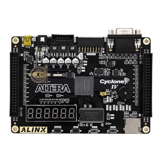
FPGA Development Board AX301 User Manual Table of Contents Version Record ..................2 Part 1: FPGA Development Board Introduction .......... 5 Part 2: Power Supply .................. 7 Part 3: FPGA ....................8 Part 3.1: JTAG Interface ..............9 Part 3.2: FPGA power and GND pins ..........10 Part 4: 50M Active Crystal ................ - Page 4 FPGA Development Board AX301 User Manual The ALINX AX301 development board is an entry-level product for ALTERA FPGAs and is primarily targeted at FPGA beginners. AX301 uses ALTERA's Cyclone IV series chip, the model is EP4CE6F17C8, and it is a 256-pin FBGA package.
-
Page 5: Part 1: Fpga Development Board Introduction
FPGA Development Board AX301 User Manual Part 1: FPGA Development Board Introduction The AX301 development board uses ALTERA's Cyclone IV series FPGA, the model is EP4CE6F17C8, and a 256-pin FBGA package. The resources of this FPGA are shown below: The main parameters as below:... - Page 6 50M active crystal on board, providing stable clock source for development board Two 40-pin ALINX standard expansion ports (2.54mm pitch), of which 34 IO ports, one 5V power supply, two 3.3V power supplies, and three GND. Two expansion modules can be connected at the same time, Amazon Store: https://www.amazon.com/alinx...
-
Page 7: Part 2: Power Supply
6 digits dynamically Part 2: Power Supply The AX301 development board is powered by USB. Use a MINI USB cable to connect the development board to the computer's USB and press the power switch to power the development board. The power supply design... -
Page 8: Part 3: Fpga
Figure 2-2: Test Points for Power supply on the Board Part 3: FPGA The FPGA model used by the AX301 development board is EP4CE6F17C8, which belongs to ALTERA's Cyclone IV. This model is a BGA package with 256 pins. The definition of FPGA pins is explained again. Many people use FPGAs that are non-BGA packages, such as 144-pin, 208-pin FPGA chips. -
Page 9: Part 3.1: Jtag Interface
FPGA Development Board AX301 User Manual Figure 3-1: The FPGA chip on the Board Part 3.1: JTAG Interface First of all, let's talk about the configuration and debugging interface of FPGA: JTAG interface. The function of the JTAG interface is to download the compiled program (.sof) into the FPGA or the FLASH configuration program... -
Page 10: Part 3.2: Fpga Power And Gnd Pins
FPGA Development Board AX301 User Manual development board. Figure 3-2: The JTAG port schematic The JTAG interface uses a 10-pin 2.54mm standard connector. Figure 3-3 is the JTAG interface on the development board. Figure 3-3: The JTAG port on the FPGA Board Part 3.2: FPGA power and GND pins... - Page 11 FPGA Development Board AX301 User Manual FPGA. Among them, VCCIO0 is the power supply pin of FPGA BANK0. Similarly, VCCIO1 ~ VCCIO3 are the power supply pins of FPGA BANK ~ BANK3 respectively. In the development board, VCCIO is connected to 3.3V voltage.
-
Page 12: Part 4: 50M Active Crystal
FPGA Development Board AX301 User Manual Figure 3-5: FPGA GND Pin Part 4: 50M Active Crystal Figure 4-1 is a 50M active crystal circuit that provides a clock source for the development board. Crystal output is connected to FPGA global input clock pin (CLK1 pin E1). -
Page 13: Part 5: Spi Flash
FPGA Pin Part 5: SPI Flash The AX301 FPGA development board is equipped with a 16Mbit SPI FLASH chip, model W25P16, which uses the 3.3V CMOS voltage standard and completely replaces the configuration chip EPCS16 of ALTERA. Due to its non-volatile characteristics, in use, SPI FLASH can be used as the boot image of the FPGA system. -
Page 14: Part 6: Sdram
DATA0 ASDO Part 6: SDRAM The AX301 FPGA development board has an SDRAM chip on board, model: HY57V2562GTR, capacity: 256Mbit (16M * 16bit), 16bit bus. SDRAM can be used for data buffering. For example, the data collected by the camera is temporarily stored in SDRAM and then displayed through the VGA interface. - Page 15 FPGA Development Board AX301 User Manual Figure 6-1: SDRAM schematic Figure 6-2: SDRAM on the FPGA Board Amazon Store: https://www.amazon.com/alinx 15 / 36...
- Page 16 FPGA Development Board AX301 User Manual SDRAM pin assignment: Pin Name FPGA Pin S_CLK S_CKE S_NCS S_NWE S_NCAS S_NRAS S_DQM<0> S_DQM<1> S_BA<0> S_BA<1> S_A<0> S_A<1> S_A<2> S_A<3> S_A<4> S_A<5> S_A<6> S_A<7> S_A<8> S_A<9> S_A<10> S_A<11> S_A<12> S_DB<0> S_DB<1> S_DB<2> S_DB<3>...
-
Page 17: Part 7: Eeprom 24Lc04
S_DB<15> Part 7: EEPROM 24LC04 AX301 FPGA development board contains an EEPROM, model 24LC04, and has a capacity of 4Kbit (2*256*8bit). It consists of two 256-byte blocks and communicates via the IIC bus. The EEPROM is generally used in the design of instruments and meters, and is used to store some parameters. -
Page 18: Part 8: Real-Time Clock Ds1302
FPGA Pin Part 8: Real-time clock DS1302 The AX301 FPGA development board contains a real-time clock RTC chip, model DS1302, which provides a calendar function up to 2099, with days, minutes, minutes, seconds and weeks. If time is needed in the system, then the RTC needs to be involved in the product. -
Page 19: Part 9: Usb To Serial Port
FPGA Development Board AX301 User Manual continuous time information. Figure 8-1 shows the design of the DS1302: Figure 8-1: DS1302 schematic Figure 8-12: DS1302 on the FPGA Board DS1302 interface pin assignment: Pin Name FPGA Pin RTC_SClK RTC_nRST RTC_DATA Part 9: USB to Serial Port The development board contains the Silicon Labs CP2102GM USB-UAR Amazon Store: https://www.amazon.com/alinx... - Page 20 FPGA Development Board AX301 User Manual chip. The USB interface uses the MINI USB interface. This USB interface implements the power supply function, and it can implement the USB to serial port function. You can use a USB cable to connect it to the USB port of the PC for serial data communication.
-
Page 21: Part 10: Vga Interface
FPGA Development Board AX301 User Manual At the same time, two led indicators (LED7, LED8) are set for the serial port signal. LED7 and LED8 will indicate whether there is data transmitted or received by the serial port, as shown in Figure 9-3. - Page 22 FPGA Development Board AX301 User Manual Figure 10-1: VGA video signal transmission diagram HSYNC and VSYNC are line data synchronization and frame data synchronization, respectively, and are TTL levels. FPGA can only output digital signals, and R, G, and B required by VGA are analog signals. The digital-to-analog signals of VGA are implemented by a simple resistor circuit.
- Page 23 FPGA Development Board AX301 User Manual Figure 10-2: VGA Interface Schematic Figure 10-3: VGA Interface on the FPGA Board VGA interface pin assignment Pin Name FPGA Pin Description BLUE[0] VGA_D[0] Amazon Store: https://www.amazon.com/alinx 23 / 36...
-
Page 24: Part 11: Sd Card Slot
FPGA Development Board AX301 User Manual BLUE[1] VGA_D[1] BLUE[2] VGA_D[2] BLUE[3] VGA_D[3] BLUE[4] VGA_D[4] GREEN[0] VGA_D[5] GREEN[1] VGA_D[6] GREEN[2] VGA_D[7] GREEN[3] VGA_D[8] GREEN[4] VGA_D[9] GREEN[5] VGA_D[10] RED[0] VGA_D[11] RED[1] VGA_D[12] RED[2] VGA_D[13] RED[3] VGA_D[14] RED[4] VGA_D[15] Line sync signal VGA_HS... - Page 25 FPGA Development Board AX301 User Manual Figure 11-1: SD card slot schematic Figure 11-2: SD card slot on the FPGA Board SD card slot pin assignment SD Mode FPGA Pin Pin Name SD_NCS SD_DIN SD_CLK SD_DOUT Amazon Store: https://www.amazon.com/alinx 25 / 36...
-
Page 26: Part 12: Leds
FPGA Development Board AX301 User Manual Part 12: LEDs The AX301 FPGA development board has 4 user LEDs on board. The schematic diagram of the four user LEDs is shown in Figure 12-1. When the FPGA pin output is logic 0, the LEDs will off. When the output is logic 1, the LED is lit. -
Page 27: Part 13: User Keys
FPGA Development Board AX301 User Manual Part 13: User Keys The development board has 4 independent keys, 3 user keys (KEY1 ~ KEY3), and 1 function key (RESET). Press the key to low level (0), release The schematic diagram of the four keys is shown in Figure to high level (1). -
Page 28: Part 14: Camera Module Interface
FPGA Development Board AX301 User Manual Part 14: Camera Module interface The development board includes an 18-pin CMOS camera interface, which can be connected to the OV5640 camera module to implement the video capture function. After the capture, the display can be connected to the display through a TFT LCD screen or a VGA interface. -
Page 29: Part 15: Digital Tube
FPGA Development Board AX301 User Manual Camera interface pin assignment: Pin Number FPGA Pin OV5640 camera module PIN1 +3.3V +3.3V PIN2 PIN3 CMOS_SCL PIN4 CMOS_SDA PIN5 CMOS_PCLK PIN6 CMOS_VSYNC PIN7 CMOS_D3 PIN8 CMOS_D2 PIN9 CMOS_D7 PIN10 CMOS_D6 PIN 11 CMOS_XCLK... - Page 30 FPGA Development Board AX301 User Manual Figure 15-1: Digital tube segment structure We use a common anode digital tube. When the pin corresponding to a field is low, the corresponding field is lit, and when the pin corresponding to a field is high, the corresponding field is not lit.
- Page 31 FPGA Development Board AX301 User Manual Figure 15-2: Digital tube schematic Figure 15-3: Digital tube on the FPGA Board Amazon Store: https://www.amazon.com/alinx 31 / 36...
-
Page 32: Part 16: Buzzer
FPGA Development Board AX301 User Manual Digital tube pin assignment Pin Name FPGA Pin Description Corresponding section A DIG[0] Corresponding section B DIG[1] Corresponding section C DIG[2] Corresponding section D DIG[3] Corresponding section E DIG[4] Corresponding section F DIG[5] Corresponding section G... -
Page 33: Part 17: Expansion Ports
FPGA Development Board AX301 User Manual Figure 16.-2 is the buzzer on the FPGA Development board. The yellow is the jumper connected to the buzzer and the FPGA pins. If you do not want the buzzer to sound, unplug it. - Page 34 FPGA Development Board AX301 User Manual Figure 17-1: Expansion header J1 schematic Figure 17-2: Expansion header J2 schematic Figure 17-3 is the J1 and J2 expansion ports on the FPGA Development Board. Pin1, Pin2 and Pin39, Pin40 of the expansion ports have been marked on the board.
- Page 35 FPGA Development Board AX301 User Manual Figure 17-3: J1 and J2 expansion ports J1 Expansion Header Pin Assignment Pin Number FPGA Pin Pin Number FPGA Pin VCC5V Amazon Store: https://www.amazon.com/alinx 35 / 36...
- Page 36 FPGA Development Board AX301 User Manual D3V3 D3V3 J2 Expansion Header Pin Assignment Pin Number FPGA Pin Pin Number FPGA Pin VCC5V D3V3 D3V3 Amazon Store: https://www.amazon.com/alinx 36 / 36...
Need help?
Do you have a question about the AX301 and is the answer not in the manual?
Questions and answers