Table of Contents
Advertisement
Advertisement
Table of Contents

Related Manuals for Alinx ZYNQ UltraScale+ AXU9EGB


Summary of Contents for Alinx ZYNQ UltraScale+ AXU9EGB
- Page 1 ZYNQ UltraScale+ FPGA Development Board AXU9EGB User Manual...
-
Page 2: Version Record
AXU9EGB User Manual Version Record Version Date Release By Description Rev 1.1 2021-07-21 Rachel Zhou First Release 2 / 66 www.alinx.com... -
Page 3: Table Of Contents
Part 3.9: CAN Communication Interface ..........50 Part 3.10: 485 Communication Interface ........... 50 Part 3.11: MIPI Camera Interface ............51 Part 3.12: FMC Interface ..............53 Part 3.13: 40-Pin Expansion Headers ..........58 Part 3.14: JTAG Debug Port ...............59 3 / 66 www.alinx.com... - Page 4 Part 3.16: EEPROM and Temperature Sensor ........60 Part 3.17: User LEDs ................61 Part 3.18: Keys ................... 62 Part 3.19: DIP Switch Configuration ...........63 Part 3.20: Power Supply ..............64 Part 3.21: ALINX Customized Fan ............. 65 Part 3.22: Carrier Board Size Dimension ...........66 4 / 66 www.alinx.com...
- Page 5 It is a "professional" ZYNQ development platform. For high-speed data transmission and exchange, pre-verification and post-application of data processing is possible. This product is very suitable for students, engineers and other groups engaged in MPSoCs development. 5 / 66 www.alinx.com...
- Page 6 AXU9EGB User Manual 6 / 66 www.alinx.com...
-
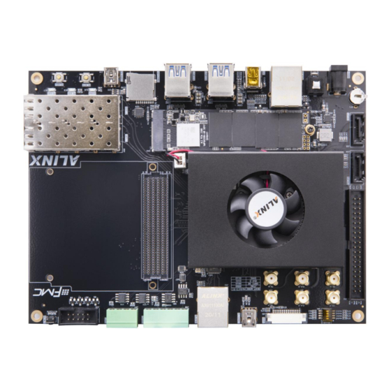
Page 7: Part 1: Fpga Development Board Introduction
Ethernet interfaces, 2 SFP Interfaces, 2 SATA Interfaces, 2 UART, 1 SD card slot, 1 FMC Interface, 2-Channel CAN bus interfaces, 2-Channel RS485 bus interfaces, 1 MIPI Camera Interface, 40-pin expansion ports and some keys and LEDs. The following figure shows the structure of the entire development system: 7 / 66 www.alinx.com... - Page 8 PS system, and a differential 200MHz crystal oscillator for the PL logic DDR reference clock. M.2 Interface 1 PCIEx1 standard M.2 interface, used to connect M.2 SSD solid state drives, with a communication speed of up to 6Gbps. DP Output Interface 8 / 66 www.alinx.com...
- Page 9 1 Micro SD card holder, used to store operating system image and file system. FMC Expansion Interface 1 standard FMC LPC expansion port, which can be connected to various FMC modules of XILINX or ALINX (HDMI input and output modules, binocular camera modules, high-speed AD modules, etc.). 9 / 66 www.alinx.com...
- Page 10 2 Lane MIPI camera input interfaces, used to connect MIPI camera module (AN5641). 40-pin Expansion Header The 40-pin 2.54mm pitch expansion port use for external ALINX modules (binocular camera, TFT LCD screen, high-speed AD module, etc.). The expansion port includes 1 channel of 5V power supply, 2 channels of 3.3V power supply, 3 channels of ground, and 34 channels...
- Page 11 There are 1 power indicator and on the core board. There are 1 power indicator,1 DONE Configuration indicator and 2 user indicators on the carrier board. KEYs 3 KEYs, include 1 Rest KEY and 2 User KEYs. 11 / 66 www.alinx.com...
-
Page 12: Part 2: Acu9Eg Core Board
IO ports on the PL side (HP I/O: 96, HD I/O: 84). The wiring between the XCZU9EG chip and the interface has been processed with equal length and differential, and the core board size is only 3.15*2.36 (inch), which is very suitable for secondary development. 12 / 66 www.alinx.com... -
Page 13: Part 2.2: Zynq Chip
PCIE Gen2, USB3.0, SATA 3.1, DisplayPort; it also supports USB2.0, Gigabit Ethernet, SD/SDIO, I2C, CAN, UART, GPIO and other interfaces. The PL end contains a wealth of programmable logic units, DSP and internal RAM. . Figure 2-2-1 detailed the Overall Block Diagram of the ZU9EG Chip. 13 / 66 www.alinx.com... - Page 14 External storage interface, support 32/64bit DDR4/3/3L, LPDDR4/3 interface Static storage interface, support NAND, 2xQuad-SPI FLASH. High-speed connection interface, support PCIe Gen2 x 4, 2 x USB3.0, Sata 3.1, Display Port, 4 x Tri-mode, Gigabit Ethernet 14 / 66 www.alinx.com...
-
Page 15: Part 2.3: Ddr4 Dram
2GB. The maximum operating speed of the DDR4 SDRAM on the PS side can reach 1200MHz (data rate 2400Mbps), and the 4 DDR4 storage systems are directly connected to the memory interface of the PS BANK504. The 15 / 66 www.alinx.com... - Page 16 The hardware connection of DDR4 SDRAM on the PS Side is shown in Figure 2-3-1: Figure 2-3-1: DDR3 DRAM schematic diagram The hardware connection of DDR4 SDRAM on the Pl Side is shown in Figure 2-3-2: 16 / 66 www.alinx.com...
- Page 17 PS_DDR4_DQS3_N PS_DDR_DQS_N3_504 AH23 PS_DDR4_DQS3_P PS_DDR_DQS_P3_504 AH22 PS_DDR4_DQS4_N PS_DDR_DQS_N4_504 AH29 PS_DDR4_DQS4_P PS_DDR_DQS_P4_504 AH28 PS_DDR4_DQS5_N PS_DDR_DQS_N5_504 AE29 PS_DDR4_DQS5_P PS_DDR_DQS_P5_504 AE28 PS_DDR4_DQS6_N PS_DDR_DQS_N6_504 AK32 PS_DDR4_DQS6_P PS_DDR_DQS_P6_504 AJ32 PS_DDR4_DQS7_N PS_DDR_DQS_N7_504 AE33 PS_DDR4_DQS7_P PS_DDR_DQS_P7_504 AE32 PS_DDR4_DQ0 PS_DDR_DQ0_504 AP20 PS_DDR4_DQ1 PS_DDR_DQ1_504 AP18 17 / 66 www.alinx.com...
- Page 18 PS_DDR4_DQ26 PS_DDR_DQ26_504 AG24 PS_DDR4_DQ27 PS_DDR_DQ27_504 AG23 PS_DDR4_DQ28 PS_DDR_DQ28_504 AK22 PS_DDR4_DQ29 PS_DDR_DQ29_504 AJ21 PS_DDR4_DQ30 PS_DDR_DQ30_504 AJ22 PS_DDR4_DQ31 PS_DDR_DQ31_504 AK23 PS_DDR4_DQ32 PS_DDR_DQ32_504 AG31 PS_DDR4_DQ33 PS_DDR_DQ33_504 AG30 PS_DDR4_DQ34 PS_DDR_DQ34_504 AG29 PS_DDR4_DQ35 PS_DDR_DQ35_504 AG28 PS_DDR4_DQ36 PS_DDR_DQ36_504 AJ30 PS_DDR4_DQ37 PS_DDR_DQ37_504 AK29 18 / 66 www.alinx.com...
- Page 19 PS_DDR4_DQ62 PS_DDR_DQ62_504 AD34 PS_DDR4_DQ63 PS_DDR_DQ63_504 AD33 PS_DDR4_DM0 PS_DDR_DM0_504 AG20 PS_DDR4_DM1 PS_DDR_DM0_504 AN17 PS_DDR4_DM2 PS_DDR_DM1_504 AM21 PS_DDR4_DM3 PS_DDR_DM2_504 AK19 PS_DDR4_DM4 PS_DDR_DM3_504 AH24 PS_DDR4_DM5 PS_DDR_DM4_504 AH31 PS_DDR4_DM6 PS_DDR_DM5_504 AE30 PS_DDR4_DM7 PS_DDR_DM6_504 AJ31 PS_DDR4_A0 PS_DDR_A0_504 AP29 PS_DDR4_A1 PS_DDR_A1_504 AP30 19 / 66 www.alinx.com...
- Page 20 PS_DDR_PARITY_504 AF20 PS_DDR4_RESET_B PS_DDR_RST_N_504 AF21 PS_DDR4_CLK0_P PS_DDR_CK0_504 AN26 PS_DDR4_CLK0_N PS_DDR_CK_N0_504 AN27 PS_DDR4_CKE0 PS_DDR_CKE0_504 AN29 PL Side DDR4 DRAM pin assignment: Signal Name Pin Name Pin Number PL_DDR4_DQS0_N IO_L22N_T3U_N7_DBC_AD0N_65 PL_DDR4_DQS0_P IO_L22P_T3U_N6_DBC_AD0P_65 PL_DDR4_DQS1_N IO_L16N_T2U_N7_QBC_AD3N_65 PL_DDR4_DQS1_P IO_L16P_T2U_N6_QBC_AD3P_65 PL_DDR4_DQS2_N IO_L10N_T1U_N7_QBC_AD4N_65 20 / 66 www.alinx.com...
- Page 21 PL_DDR4_DQ18 IO_L11P_T1U_N8_GC_65 PL_DDR4_DQ19 IO_L12N_T1U_N11_GC_65 PL_DDR4_DQ20 IO_L9P_T1L_N4_AD12P_65 PL_DDR4_DQ21 IO_L8N_T1L_N3_AD5N_65 PL_DDR4_DQ22 IO_L12P_T1U_N10_GC_65 PL_DDR4_DQ23 IO_L11N_T1U_N9_GC_65 PL_DDR4_DQ24 IO_L3P_T0L_N4_AD15P_65 AE12 PL_DDR4_DQ25 IO_L5N_T0U_N9_AD14N_65 PL_DDR4_DQ26 IO_L2N_T0L_N3_65 AH11 PL_DDR4_DQ27 IO_L6N_T0U_N11_AD6N_65 PL_DDR4_DQ28 IO_L2P_T0L_N2_65 AH12 PL_DDR4_DQ29 IO_L5P_T0U_N8_AD14P_65 AG10 PL_DDR4_DQ30 IO_L3N_T0L_N5_AD15N_65 AF12 PL_DDR4_DQ31 IO_L6P_T0U_N10_AD6P_65 AD10 PL_DDR4_DM0 IO_L19P_T3L_N0_DBC_AD9P_65 21 / 66 www.alinx.com...
-
Page 22: Part 2.4: Qspi Flash
Part 2.4: QSPI Flash The FPGA core board ACU9EG is equipped with two 256MBit Quad-SPI FLASH chip to form an 8-bit bandwidth data bus, the flash model is MT25QU256ABA1EW9, which uses the 1.8V CMOS voltage standard. Due to 22 / 66 www.alinx.com... - Page 23 PS ports need to be configured as the QSPI FLASH interface. Figure 2-4-1 shows the QSPI Flash in the schematic. Figure 2-4-1: QSPI Flash in the schematic Configure chip pin assignments: Signal Name Pin Name Pin Number MIO5_QSPI0_SS_B PS_MIO5_500 AM15 23 / 66 www.alinx.com...
-
Page 24: Part 2.5: Emmc Flash
PS part of the ZYNQ UltraScale+. In the system design, it is necessary to configure the GPIO port function of the PS side as an EMMC interface. Figure 2-5-1 shows the part of eMMC Flash in the schematic diagram. 24 / 66 www.alinx.com... -
Page 25: Part 2.6: Clock Configuration
The core board provides reference clock and RTC real-time clock for PS system and PL logic respectively, so that PS system and PL logic can work independently. The schematic diagram of the clock circuit design is shown in Figure 2-6-1: 25 / 66 www.alinx.com... - Page 26 PS system. The crystal is connected to the PS_PADI_503 and PS_PADO_503 pins of BANK503 of the ZYNQ chip. The schematic diagram is shown in Figure 2-6-2: Figure 2-6-2: Passive Crystal Oscillator for RTC Clock pin assignment: Signal Name PS_PADI_503 PS_PADO_503 26 / 66 www.alinx.com...
- Page 27 (MRCC) of PL BANK64. This global clock can be used to drive the DDR4 controller and user logic circuits in the FPGA. The schematic diagram of this clock source is shown in Figure 2-6-4 27 / 66 www.alinx.com...
-
Page 28: Part 2.7: Power Supply
XCZU9EG with 0.85V. In addition, a PMIC chip TPS6508640 is used to generate all other power supplies required by the XCZU9EG chip. For the TPS6508640 power supply design, please refer to the power supply chip manual. The design block diagram is as follows : 28 / 66 www.alinx.com... - Page 29 AXU9EGB User Manual 29 / 66 www.alinx.com...
-
Page 30: Part 2.8: Acu9Eg Core Board Size Dimension
J29 connects the IO of BANK66, BANK67 and the GTX signal of BANK228; the level standard of BANK66, 67 is determined by the VCCO_66 and VCCO_67 power supply of the carrier board, the carrier board provides +1.8V by default. Pin assignment of board to board connector J29 30 / 66 www.alinx.com... - Page 31 B66_L19_N B66_L11_P B67_L16_P B67_L6_P B67_L16_N B67_L6_N B67_L19_N B66_L14_N B67_L19_P B66_L14_P B66_L9_P B66_L21_P B66_L9_N B66_L21_N B67_L8_P B67_L21_N B67_L8_N B67_L21_P B67_L5_P B67_L24_N B67_L5_N B67_L24_P B66_L22_N B66_L13_P B66_L22_P B66_L13_N B66_L24_N B67_L4_P B66_L24_P B67_L4_N B67_L20_P B67_L22_P B67_L20_N B67_L22_N B67_L23_N B67_L17_P 31 / 66 www.alinx.com...
- Page 32 J30 is connected to the transceiver signal of BANK505 MGT, MIO of PS, VCCO_66, VCCO_67 and +12V power supply. The MIO level of PS is 1.8V standard J29 Pin Signal Name J29 Pin Signal Name Number Number 505_TX0_P AB29 505_CLK0_P AA27 505_TX0_N AB30 505_CLK0_N AA28 32 / 66 www.alinx.com...
- Page 33 505_CLK3_P 505_TX1_N 505_CLK3_N 505_TX1_P PS_MIO26 USB_STP PS_MIO35 USB_DIR PS_MIO28 USB_CLK PS_MIO37 USB_NXT PS_MIO39 USB_DATA0 PS_MIO27 USB_DATA1 PS_MIO40 USB_DATA2 PS_MIO30 USB_DATA3 PS_MIO34 USB_DATA4 PS_MIO29 USB_DATA5 PS_MIO31 USB_DATA6 PS_MIO32 USB_DATA7 PS_MIO42 PHY1_MDC PS_MIO36 PHY1_MDIO PS_MIO33 PHY1_TXD0 PS_MIO38 PHY1_TXD1 33 / 66 www.alinx.com...
- Page 34 BANK66, 67 is determined by the VCCO_66 and VCCO_67 power supply of the carrier board, the carrier board provides +1.8V by default. J31 Pin Signal Name J31 Pin Signal Name Number Number FPGA_TCK POWER_SW FPGA_TMS PS_MODE3 FPGA_TDO PS_MODE2 FPGA_TDI 34 / 66 www.alinx.com...
- Page 35 B44_L11_P AF15 B44_L6_N AL12 B44_L1_N AP14 B44_L2_N AN13 B44_L1_P AN14 B44_L2_P AM14 B44_L3_N AP12 B44_L3_P AN12 B44_L4_N AM13 B44_L4_P AL13 B44_L10_P AG14 B44_L10_N AG13 B50_L8_N B44_L9_N AF13 B50_L8_P B44_L9_P AE13 B50_L7_N B50_L6_P B50_L7_P B50_L6_N B50_L5_N B50_L5_P 35 / 66 www.alinx.com...
- Page 36 J32 connects the IO of BANK47, 48, 49 and the transceiver signal of BANK128, 129, 130. J32 Pin Signal Name Pin Number J32 Pin Signal Name Pin Number B48_L5_P B48_L10_N B48_L5_N B48_L10_P B48_L11_P B49_L9_N B48_L11_N B49_L9_P B49_L8_N B47_L12_N B49_L8_P B47_L12_P B47_L11_N B49_L4_N B47_L11_P B49_L4_P 36 / 66 www.alinx.com...
- Page 37 130_TX3_N 130_RX2_N 130_TX3_P 130_RX2_P 130_RX0_N 130_RX1_N 130_RX0_P 130_RX1_P 130_TX0_N 130_TX1_N 130_TX0_P 130_TX1_P 130_CLK0_N 130_CLK1_N 130_CLK0_P 130_CLK1_P 129_TX3_N 129_RX3_N 129_TX3_P 129_RX3_P 129_RX1_N 129_TX2_N 129_RX1_P 129_TX2_P 129_TX1_N 129_RX2_N 129_TX1_P 129_RX2_P 129_RX0_N 129_TX0_N 129_RX0_P 129_TX0_P 129_CLK0_N 129_CLK1_N 129_CLK0_P 129_CLK1_P 37 / 66 www.alinx.com...
- Page 38 AXU9EGB User Manual 128_TX3_N 128_RX3_N 128_TX3_P 128_RX3_P 128_TX2_N 128_RX1_P 128_TX2_P 128_RX1_N 128_TX0_N 128_RX0_P 128_TX0_P 128_RX0_N 128_TX1_N 128_RX2_P 128_TX1_P 128_RX2_N 128_CLK0_N 128_CLK1_P 128_CLK0_P 128_CLK1_N 38 / 66 www.alinx.com...
-
Page 39: Part 3: Carrier Board
6Gbps. The M.2 interface uses the M key slot, which only supports PCI-E, not SATA. When users choose SSD solid state drives, they need to choose PCIE type SSD solid state drives. 39 / 66 www.alinx.com... -
Page 40: Part 3.3: Dp Interface
505_PCIE_REFCLK_N 505_CLK0_N AA28 PCIE Reference Clock Negative PCIE_RSTn_MIO37 PS_MIO37 PCIE Reset Signal Part 3.3: DP Interface The AXU9EGB FPGA development board has a standard DisplayPort output display interface for video image display. The interface supports VESA 40 / 66 www.alinx.com... - Page 41 505_TX3_P Transmit Positive Low bits of DP Data GT0_DP_TX_N 505_TX3_N Transmit Negative High bits of DP Data GT1_DP_TX_P 505_TX2_P Transmit Positive High bits of DP Data GT1_DP_TX_N 505_TX2_N Transmit Negative DP Reference Clock 505_DP_CLKP 505_CLK2_P Positive 41 / 66 www.alinx.com...
-
Page 42: Part 3.4: Usb3.0 Interface
USB Slave peripherals (such as USB mouse, keyboard or U disk) at the same time. The schematic diagram of USB3.0 connection is shown as 3-4-1: Figure 3-4-1: USB3.0 Interface Schematic 42 / 66 www.alinx.com... -
Page 43: Part 3.5: Gigabit Ethernet Interface
JL2121-N040I chip supports 10/100/1000 Mbps network transmission rate, and communicates with the MAC layer of the ZU9EG system through the RGMII interface. JL2121-N040I supports MDI/MDX adaptation, various speed adaptation, Master/Slave adaptation, and MDIO bus for PHY register management. 43 / 66 www.alinx.com... - Page 44 When the network is connected to 100M Ethernet, the data transmission of ZYNQ and PHY chip JL2121-N040I is communicated through RMII bus, and the transmission clock is 25Mhz. Data is sampled on the rising edge and falling samples of the clock. 44 / 66 www.alinx.com...
- Page 45 PHY1_RXD3 PS_MIO74 Ethernet 1 Receive Data Bit3 PHY1_RXCTL PS_MIO75 Ethernet 1 Receive Enable Signal PHY1_MDC PS_MIO76 Ethernet 1 MDIO Clock Management PHY1_MDIO PS_MIO77 Ethernet 1 MDIO Management Data PL Gigabit Ethernet pin assignment is as follows 45 / 66 www.alinx.com...
-
Page 46: Part 3.6: Usb To Serial Port
PC's USB port for serial data communication. The schematic diagram of the USB Uart circuit design is shown in the figure below: The schematic diagram of the USB Uart circuit design is shown in Figure 3-6-1: 46 / 66 www.alinx.com... -
Page 47: Part 3.7: Sd Card Slot Interface
ZU9EG. Since the VCCMIO of the BANK is set to 1.8V, but the data level of the SD card is 3.3V, connected through the TXS02612 level shifter. The schematic of the ZU9EG PS and SD card connector is shown in Figure 3-7-1: 47 / 66 www.alinx.com... -
Page 48: Part 3.8: Sfp Interface
GNK transceiver of ZYNQ BANK228, and the data rate of each TX transmission and RX reception is up to 12.5Gb/s. The reference clock of the GTH transceiver is provided by the 125M differential clock of the core board. The SFP Schematic detailed is shown in Figure 3-8-1: 48 / 66 www.alinx.com... - Page 49 SFP1_TX_DIS B50_L8_N High Level (Positive) Enable Optical Module 2 Light Emission Prohibited, SFP2_TX_DIS B50_L7_N High Level (Positive) Enable Optical Module 1 Receive LOSS SFP1_LOSS B50_L8_P Detect Signal Optical Module 2 Receive LOSS SFP2_LOSS B50_L7_P Detect Signal 49 / 66 www.alinx.com...
-
Page 50: Part 3.9: Can Communication Interface
PS_CAN2_TX PS_MIO40 CAN2 Transmitter PS_CAN2_RX PS_MIO41 CAN2 Receiver Part 3.10: 485 Communication Interface There are two 485 communication interfaces on the AXU9EGB carrier board. The 485 communication port 1 is connected to the IO interface of 50 / 66 www.alinx.com... -
Page 51: Part 3.11: Mipi Camera Interface
Part 3.11: MIPI Camera Interface The AXU9EGB carrier board includes a MIPI camera interface, which can be used to connect with the ALINX Brand MIPI OV5640 camera module AN5641. MIPI interface 15PIN FPC connector, 2 LANE data and 1 pair of clock,... - Page 52 MIPI Input Date LANE0 Positive MIPI_LAN0_N B67_L2_N MIPI Input Date LANE0 Negative MIPI_LAN1_P B67_L3_P MIPI Input Date LANE1 Positive MIPI_LAN1_N B67_L3_N MIPI Input Date LANE1 Negative CAM_GPIO B44_L6_P AK13 GPIO Control of Camera CAM_CLK B44_L6_N AL12 Clock Input of Camera 52 / 66 www.alinx.com...
-
Page 53: Part 3.12: Fmc Interface
Part 3.12: FMC Interface The AXU9EGB FPGA Carrier board has a standard FMC HPC expansion port that can be connected to various FMC modules of XILINX or ALINX (HDMI input and output modules, binocular camera modules, high-speed AD modules, etc.). The FMC expansion port contains 36 pairs of differential IO signals and 8 pairs of GTX Transceivers. - Page 54 FMC Transceiver Data Transmission 4 FMC_DP4_C2M_N 129_TX0_N Negative FMC Transceiver Data Transmission 5 FMC_DP5_C2M_P 129_TX1_P Positive FMC Transceiver Data Transmission 5 FMC_DP5_C2M_N 129_TX1_N Negative FMC Transceiver Data Transmission 6 FMC_DP6_C2M_P 129_TX2_P Positive FMC Transceiver Data Transmission 6 FMC_DP6_C2M_N 129_TX2_N Negative 54 / 66 www.alinx.com...
- Page 55 FMC Transceiver Data Receive 6 FMC_DP6_M2C_P 129_RX2_P Positive FMC Transceiver Data Receive 6 FMC_DP6_M2C_N 129_RX2_N Negative FMC Transceiver Data Receive 7 FMC_DP7_M2C_P 129_RX3_P Positive FMC Transceiver Data Receive 7 FMC_DP7_M2C_N 129_RX3_N Negative FMC_CLK0_P B67_L14_P FMC Reference 1 Clock P 55 / 66 www.alinx.com...
- Page 56 Data N FMC_LA14_P B67_L21_P FMC Reference 14 Data P FMC_LA14_N B67_L21_N FMC Reference 14 Data N FMC_LA15_P B67_L5_P FMC Reference 15 Data P FMC_LA15_N B67_L5_N FMC Reference 15 Data N FMC_LA16_P B67_L16_P FMC Reference 16 Data P 56 / 66 www.alinx.com...
- Page 57 Data N FMC_LA32_P B66_L20_P FMC Reference 32 Data P FMC_LA32_N B66_L20_N FMC Reference 32 Data N FMC_LA33_P B66_L15_P FMC Reference 33 Data P FMC_LA33_N B66_L15_N FMC Reference 33 Data N FMC_PRSNT B50_L3_P FMC Module Exist Signal 57 / 66 www.alinx.com...
-
Page 58: Part 3.13: 40-Pin Expansion Headers
Part 3.13: 40-Pin Expansion Headers The carrier board is reserved with one 0.1inch spacing standard 40-pin expansion ports J50, which is used to connect the ALINX modules or the external circuit designed by the user. The expansion port has 40 signals, of which 1-channel 5V power supply, 2-channel 3.3 V power supply, 3-channle... -
Page 59: Part 3.14: Jtag Debug Port
External need to connect a 32.768KHz passive clock to provide an accurate clock source to the internal clock circuit, so that the RTC can accurately provide 59 / 66 www.alinx.com... -
Page 60: Part 3.16: Eeprom And Temperature Sensor
Semiconductor. The temperature accuracy of the LM75 chip is 0.5 degrees. The EEPROM and temperature sensor are mounted on the Bank500 MIO of ZYNQ UltraScale+ through the I2C bus. Figure 3-16-1 is the schematic diagram of EEPROM and temperature sensor 60 / 66 www.alinx.com... -
Page 61: Part 3.17: User Leds
1 DONE indicator, 1 PS control indicator, and 1 PL control indicator. The user can control the on and off through the program. The schematic diagram of the user's LED light hardware connection is shown in Figure 3-17-1: 61 / 66 www.alinx.com... -
Page 62: Part 3.18: Keys
One user KEY is connected to the MIO of the PS, and one is connected to the IO of the PL. The reset KEY and the user KEYs are both low-level active. The connection diagram of the user key is shown in Figure 3-18-1: 62 / 66 www.alinx.com... -
Page 63: Part 3.19: Dip Switch Configuration
The user can select different startup modes through the DIP switch SW1 on the expansion board. The SW1 startup mode configuration is shown in the following table 3-19-1. MODE[3:0] Start mode Dial Position (1, 2, 3, 4) 0000 PS JTAG ON,ON,ON,ON 63 / 66 www.alinx.com... -
Page 64: Part 3.20: Power Supply
Figure 3-20-1: Figure 3-20-1: Carrier Board Power Schematic The functions of each power distribution are shown in the following table: Power Function +5.0V USB power supply +1.8V Ethernet, USB2.0, BANK66,67 of Core Board 64 / 66 www.alinx.com... -
Page 65: Part 3.21: Alinx Customized Fan
Ethernet, USB2.0, SD, DP, CAN, RS485 +1.2V Ethernet Part 3.21: ALINX Customized Fan Because ZU9EG generates a lot of heat when it works normally, we add a heat sink and fan to the chip on the board to prevent the chip from overheating. -
Page 66: Part 3.22: Carrier Board Size Dimension
AXU9EGB User Manual Part 3.22: Carrier Board Size Dimension Figure 3-22-1: Top View 66 / 66 www.alinx.com...
Need help?
Do you have a question about the ZYNQ UltraScale+ AXU9EGB and is the answer not in the manual?
Questions and answers