Table of Contents
Advertisement
Quick Links
Advertisement
Table of Contents

Related Manuals for Alinx KINTEX-7 FPGA


Summary of Contents for Alinx KINTEX-7 FPGA
- Page 1 KINTEX-7 FPGA Development Board AV7K300 User Manual...
-
Page 2: Version Record
KINTEX-7 FPGA Development Board AV7K300 User Manual Version Record Version Date Release By Rev 1.1 2022-09-07 2 / 41 www.alinx.com... -
Page 3: Table Of Contents
KINTEX-7 FPGA Development Board AV7K300 User Manual Table of Contents Version Record ..................... 2 Part 1: FPGA Development Board Introduction ...........5 Part 2: AC7K325B Core Board ..............8 Part 2.1: AC7K325 Core Board Introduction ........8 Part 2.2: FPGA Chip ................9 Part 2.3: DDR3 DRAM ................ - Page 4 KINTEX-7 FPGA Development Board AV7K300 User Manual The AV7K300 FPGA development board, it is the XILINX KINTEX-7 FPGA development platform. The AV7K300 FPGA development platform uses XILINX's KINTEX-7 chip XC7K325 solution. The FPGA development board mounts four pieces of 512MB high-speed DDR3 SDRAM chips, and a 128Mb QSPI FLASH chip.
-
Page 5: Part 1: Fpga Development Board Introduction
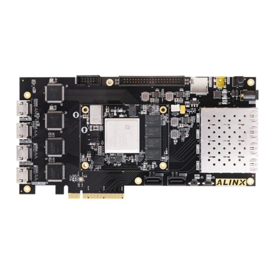
KINTEX-7 FPGA Development Board AV7K300 User Manual Part 1: FPGA Development Board Introduction The entire structure of the development board is designed by inheriting our usual core board + expansion board model. Use high-speed inter-board connectors to connect between the core board and the expansion board. - Page 6 KINTEX-7 FPGA Development Board AV7K300 User Manual Through this diagram, you can see the interfaces and functions that the AV7K300 FPGA Development Board contains: FPGA Core Board The smallest system consisting of XC7K325 + 4 DDR3 + QSPI FLASH,...
- Page 7 KINTEX-7 FPGA Development Board AV7K300 User Manual 1 Uart to USB interface, used for communication with computer, convenient for users to debug. The serial port chip adopts Silicon Labs CP2102GM USB-UART chip, and the USB interface adopts MINI USB interface.
-
Page 8: Part 2: Ac7K325B Core Board
KINTEX-7 FPGA Development Board AV7K300 User Manual Part 2: AC7K325B Core Board Part 2.1: AC7K325 Core Board Introduction AC7K325B (core board model, the same below) FPGA core board, it is based on XILINX Kintex-7 XC7K325 series chip XC7K325TFFG900100T. The core board uses 4 Micron's 512MB DDR3 chips MT41J256M16HA-125, with a total capacity of 2GB. -
Page 9: Part 2.2: Fpga Chip
Xilinx's KINTEX-7 series. The speed grade is 2, and the temperature grade is industry grade. This model is a FGG900 package with 900 pins. Xilinx KINTEX-7 FPGA chip naming rules as below Figure 2.2-1: The Specific Chip Model Definition of Kintex-7 Series Figure 2.2-2: FPGA chip on board... -
Page 10: Part 2.3: Ddr3 Dram
KINTEX-7 FPGA Development Board AV7K300 User Manual Part 2.3: DDR3 DRAM The FPGA core board AC7K325B is equipped with four Micron 4Gbit (512MB) DDR3 chips, model MT41J256M16HA-125 (compatible with MT41K256M16HA-125). Four DDR3 SDRAMs make up a 64-bit bus width. Because 4 DDR3 chips are connected to the HP port of the FPGA, the maximum operating speed of DDR3 SDRAM can reach 800MHz (data rate 1600Mbps). - Page 11 KINTEX-7 FPGA Development Board AV7K300 User Manual Net Name FPGA PIN Name FPGA P/N DDR3_D0 IO_L13P_T2_MRCC_32 AD18 DDR3_D1 IO_L16N_T2_32 AB18 DDR3_D2 IO_L14P_T2_SRCC_32 AD17 DDR3_D3 IO_L17P_T2_32 AB19 DDR3_D4 IO_L14N_T2_SRCC_32 AD16 DDR3_D5 IO_L17N_T2_32 AC19 DDR3_D6 IO_L13N_T2_MRCC_32 AE18 DDR3_D7 IO_L18P_T2_32 AB17 DDR3_D8 IO_L8P_T1_32...
- Page 12 KINTEX-7 FPGA Development Board AV7K300 User Manual DDR3_D34 IO_L22P_T3_34 DDR3_D35 IO_L19P_T3_34 DDR3_D36 IO_L24N_T3_34 DDR3_D37 IO_L23N_T3_34 DDR3_D38 IO_L24P_T3_34 DDR3_D39 IO_L20N_T3_34 DDR3_D40 IO_L10P_T1_34 DDR3_D41 IO_L8N_T1_34 DDR3_D42 IO_L11P_T1_SRCC_34 DDR3_D43 IO_L8P_T1_34 DDR3_D44 IO_L12P_T1_MRCC_34 DDR3_D45 IO_L10N_T1_34 DDR3_D46 IO_L11N_T1_SRCC_34 DDR3_D47 IO_L7N_T1_34 DDR3_D48 IO_L13P_T2_MRCC_34 DDR3_D49 IO_L16N_T2_34 DDR3_D50...
- Page 13 KINTEX-7 FPGA Development Board AV7K300 User Manual DDR3_DM5 IO_L7P_T1_34 DDR3_DM6 IO_L18P_T2_34 DDR3_DM7 IO_L1P_T0_34 DDR3_DQS0_P IO_L15P_T2_DQS_32 DDR3_DQS0_N IO_L15N_T2_DQS_32 DDR3_DQS1_P IO_L9P_T1_DQS_32 AJ18 DDR3_DQS1_N IO_L9N_T1_DQS_32 AK18 DDR3_DQS2_P IO_L3P_T0_DQS_32 AH16 DDR3_DQS2_N IO_L3N_T0_DQS_32 AJ16 DDR3_DQS3_P IO_L21P_T3_DQS_32 AC16 DDR3_DQS6_N IO_L15N_T2_DQS_34 DDR3_DQS7_P IO_L3P_T0_DQS_34 DDR3_DQS7_N IO_L3N_T0_DQS_34 DDR3_A0 IO_L1P_T0_33...
-
Page 14: Part 2.4: Qspi Flash
KINTEX-7 FPGA Development Board AV7K300 User Manual DDR3_CKE0 IO_L12P_T1_MRCC_33 AD12 DDR3_ODT IO_L12N_T1_MRCC_33 AD11 DDR3_CLK0_P IO_L13P_T2_MRCC_33 AG10 DDR3_CLK0_N IO_L13N_T2_MRCC_33 AH10 DDR3_RESET IO_L4P_T0_33 Part 2.4: QSPI Flash The FPGA core board AX7K325 is equipped with one 128MBit QSPI FLASH, and the model is W25Q128A, which uses the 3.3V CMOS voltage standard. -
Page 15: Part 2.5: Clock Configuration
KINTEX-7 FPGA Development Board AV7K300 User Manual Net Name FPGA PIN Name FPGA P/N FPGA_CCLK CCLK_0 FLASH_CE_B IO_L6P_T0_FCS_B_14 FLASH_D0 IO_L1P_T0_D00_MOSI_14 FLASH_D1 IO_L1N_T0_D01_DIN_14 FLASH_D2 IO_L2P_T0_D02_14 FLASH_D3 IO_L2N_T0_D03_14 Part 2.5: Clock Configuration The AC7K325B core board is equipped with two Sitime active differential crystals, one is 200MHz, the model is SiT9102-200.00MHz, the system main... -
Page 16: Part 2.5.2: Gtx Reference Clock
KINTEX-7 FPGA Development Board AV7K300 User Manual Figure 2.5-2: System clock source 200Mhz Differential Clock Pin Assignment Signal Name FPGA PIN SYS_CLK_P AE10 SYS_CLK_N AF10 Part 2.5.2: GTX Reference Clock G2 in Figure 2.5-3 is the 125Mhz active differential crystal. The reference clock is connected to the reference clock input REFCLK1P / REFCLK1N of BANK117. -
Page 17: Part 2.6: Led Light On Core Board
KINTEX-7 FPGA Development Board AV7K300 User Manual Net Name FPGA PIN BANK117_CLK1_P BANK117_CLK1_N Part 2.6: LED Light on Core Board There are 2 red LED lights on the AC7K325B FPGA core board, one of which is the power indicator light (PWR), one is the configuration LED light (DONE). - Page 18 KINTEX-7 FPGA Development Board AV7K300 User Manual Figure 2.7-1: Power Interface in Schematic + 5V generates + 1.0V FPGA core power through the DCDC power chip MYMGK1R820FRSR. The output current of the MYMGK1R820FRSR is as high as 20A, which far meets the core voltage current demand. The + 5V power is generated by the DCDC chip ETA1471 to generate four power sources: + 1.5V, + 3.3V, +1.8V,+ 1.5V and MGTAVTT.
-
Page 19: Part 2.8: Size Dimension
KINTEX-7 FPGA Development Board AV7K300 User Manual standards. Because the power supply of the FPGA requires the power-on sequence, in the circuit design, according to the power requirements of the chip, the power-on sequence is + 1.0V-> + 1.8V-> (+ 1.5 V, + 3.3V, VCCIO17, VCCIO18, Ensure that the chip works properly. - Page 20 KINTEX-7 FPGA Development Board AV7K300 User Manual and BANK16, J32 is connected to the IO of BANK12 and BANK13 and + 5V power. Pin assignment of J29 connector J29 Pin Signal Name FPGA Pin J29 Pin Signal Name FPGA Pin...
- Page 21 KINTEX-7 FPGA Development Board AV7K300 User Manual BANK117_TX0_N BANK118_TX0_N BANK117_TX0_P BANK118_TX0_P BANK117_RX0_N BANK118_RX0_N BANK117_RX0_P BANK118_RX0_P BANK117_TX1_N BANK118_TX1_N BANK117_TX1_P BANK118_TX1_P BANK117_RX1_N BANK118_RX1_N BANK117_RX1_P BANK118_RX1_P BANK117_TX2_N BANK118_TX2_N BANK117_TX2_P BANK118_TX2_P BANK117_RX2_N BANK118_RX2_N BANK117_RX2_P BANK118_RX2_P BANK117_TX3_N BANK118_TX3_N BANK117_TX3_P BANK118_TX3_P BANK117_RX3_N BANK118_RX3_N BANK117_RX3_P BANK118_RX3_P BANK117_CLK0_N...
- Page 22 KINTEX-7 FPGA Development Board AV7K300 User Manual B18_L5_N B18_L3_N B18_L6_P B18_L2_P B18_L6_N B18_L2_N B18_L7_P B18_L1_P B18_L7_N B18_L1_N B18_L8_P B18_L4_P B18_L8_N B18_L4_N B18_L9_P B18_L12_P B18_L9_N B18_L12_N B18_L16_P B18_L10_P B18_L16_N B18_L10_N B18_L18_P B18_L20_P B18_L18_N B18_L20_N B18_L15_P B18_L11_P B18_L15_N B18_L11_N B18_L23_P B18_L21_P B18_L23_N...
- Page 23 KINTEX-7 FPGA Development Board AV7K300 User Manual B17_L22_P B17_L21_N B17_L8_P B17_L13_P B17_L8_N B17_L13_N B17_L24_P B17_L23_N B17_L24_N B17_L23_P B17_L18_N B17_L12_P B17_L18_P B17_L12_N B17_L19_N B17_L11_N B17_L19_P B17_L11_P B17_L10_N B17_L9_N B17_L10_P B17_L9_P B17_L16_N B17_L7_P B17_L16_P B17_L7_N B17_L2_N B17_L3_N B17_L2_P B17_L3_P B17_L4_N FPGA_TCK B17_L4_P...
- Page 24 KINTEX-7 FPGA Development Board AV7K300 User Manual B16_L11_N B16_L7_N B16_L11_P B16_L7_P B16_L13_N B16_L18_N B16_L13_P B16_L18_P B16_L21_P B16_L14_N B16_L21_N B16_L14_P B16_L20_N B16_L22_N B16_L20_P B16_L22_P B16_L9_P B16_L5_P B16_L9_N B16_L5_N B16_L15_P B16_L24_N B16_L15_N B16_L24_P B16_L19_N B16_L23_N B16_L19_P B16_L23_P B16_L1_N B16_L17_P B16_L1_P B16_L17_N B16_L2_P...
- Page 25 KINTEX-7 FPGA Development Board AV7K300 User Manual B15_L2_N B15_L21_N B15_L2_P B15_L21_P B15_L13_P B15_L12_N B15_L13_N B15_L12_P B15_L22_N B15_L20_N B15_L22_P B15_L20_P B15_L15_N B15_L9_N B15_L15_P B15_L9_P B15_L19_N B15_L5_N B15_L19_P B15_L5_P B15_L17_N B15_L6_N B15_L17_P B15_L6_P B15_L11_N B15_L16_N B15_L11_P B15_L16_P B15_L23_N B15_L4_P B15_L23_P B15_L4_N Pin assignment of J32 connector...
- Page 26 KINTEX-7 FPGA Development Board AV7K300 User Manual B13_L21_N AG28 B13_L8_P B13_L21_P AG27 B13_L8_N AA30 B13_L15_N AK30 B13_L11_N AD28 B13_L15_P AK29 B13_L11_P AD27 B13_L17_N AJ29 B13_L7_N AC30 B13_L17_P AJ28 B13_L7_P AC29 B13_L20_N AK28 B13_L12_N AC27 B13_L20_P AJ27 B13_L12_P AB27 B13_L22_N AH27...
-
Page 27: Part 3: Carrier Board
KINTEX-7 FPGA Development Board AV7K300 User Manual B12_L20_N AH22 B12_L10_N AE21 B12_L20_P AG22 B12_L10_P AD21 B12_L19_N AF21 B12_L3_P AB22 B12_L19_P AF20 B12_L3_N AB23 B12_L11_N AF23 B12_L5_P AC20 B12_L11_P AE23 B12_L5_N AC21 Part 3: Carrier Board Part 3.1: Carrier Board Introduction... -
Page 28: Part 3.2: Sfp Interface
KINTEX-7 FPGA Development Board AV7K300 User Manual Part 3.2: SFP Interface The AV7K300 FPGA development board has four optical interfaces. Users can purchase SFP optical modules (1.25G, 2.5G, 10G optical modules on the market) and insert them into these four optical interfaces for optical data communication. -
Page 29: Part 3.3.: Pcie Card Slot
KINTEX-7 FPGA Development Board AV7K300 User Manual SFP2_TX_N BANK117_TX1_N SFP 2 Data Transmitter (Negative) SFP2_RX_P BANK117_RX1_P SFP 2 Data Receiver (Positive) SFP2_RX_N BANK117_RX1_N SFP 2 Data Receiver (Negative) SFP3_TX_P BANK117_TX2_P SFP 3 Data Transmitter (Positive) SFP3_TX_N BANK117_TX2_N SFP 3 Data Transmitter (Negative) - Page 30 KINTEX-7 FPGA Development Board AV7K300 User Manual Figure 3-3-1: PCIe Slot Design Schematic PCIex8 Interface Pin Assignment: Signal Name FPGA Pin Description Number PCIE_RX0_P BANK116_RX3_P PCIE Channel 0 Data Receive Positive PCIE_RX0_N BANK116_RX3_N PCIE Channel 0 Data Receive Negative PCIE_RX1_P...
-
Page 31: Part 3.4: Sdi Output Interface
KINTEX-7 FPGA Development Board AV7K300 User Manual PCIE_RX5_P BANK115_RX2_P PCIE Channel 5 Data Receive Positive PCIE_RX5_N BANK115_RX2_N PCIE Channel 5 Data Receive Negative PCIE_RX6_P BANK115_RX1_P PCIE Channel 6 Data Receive Positive PCIE_RX6_N BANK115_RX1_N PCIE Channel 6 Data Receive Negative PCIE_RX7_P... - Page 32 KINTEX-7 FPGA Development Board AV7K300 User Manual GTX transceiver TX of FPGA BANK118 to realize high-speed SDI video output. The hardware connection diagram of GV8500 chip and FPGA is shown in Figure 3-4-1: Figure 3-4-1: SDI Output Interface Schematic The pin assignment of the 1...
-
Page 33: Part 3.5: Sdi Input Interface
KINTEX-7 FPGA Development Board AV7K300 User Manual Part 3.5: SDI Input Interface There are 2 SDI input interfaces on the carrier board, used GV8500 SDI equalizer chips, which supports different formats of data input HDcctv 1.0, HD-SDI (ST 292), 3G_SDI (ST-424) and SD_SDI (ST259). The input interface is adaptive to video reception at three rates. -
Page 34: Part 3.6: Usb To Serial Port
KINTEX-7 FPGA Development Board AV7K300 User Manual Signal Name FPGA Pin Description Number SDI2_3G_RXN BANK118_RX1_N SDI Input Differential Signal Negative SDI2_3G_RXP BANK118_RX1_P SDI Input Differential Signal Positive Part 3.6: USB to Serial Port The AV7K300 carrier board is equipped with a Uart to USB interface for system debugging. -
Page 35: Part 3.9: 40-Pin Expansion Port
KINTEX-7 FPGA Development Board AV7K300 User Manual interface to provide users with access to SD card memory for storing pictures, music or other user data files. SDIO signal is connected with FPGA IO signal, supports SPI mode and SD mode, the SD card used is MicroSD card. The schematic diagram of FPGA and SD card connector is shown in Figure 3-7-1. - Page 36 KINTEX-7 FPGA Development Board AV7K300 User Manual spacing standard 40-pin expansion port J18, J33, which are used to connect the ALINX modules or the external circuit designed by the user. The expansion port has 40 signals, of which 1-channel 5V power supply, 2-channel 3.3 V power supply, 3-channle ground and 34 IOs.
-
Page 37: Part 3.9: Keys And Leds
KINTEX-7 FPGA Development Board AV7K300 User Manual J33 Expansion Header Pin Assignment J33 Pin Signal Name J33 Pin Signal Name Number Number IO2_1N IO2_1P IO2_2N IO2_2P IO2_3N IO2_3P IO2_4N IO2_4P IO2_5N IO2_5P IO2_6N IO2_6P IO2_7N IO2_7P IO2_8N IO2_8P IO2_9N IO2_9P... - Page 38 KINTEX-7 FPGA Development Board AV7K300 User Manual user LED will be extinguished. In addition, there are 4 user buttons on the board. The default button signal is high. When the button is pressed, the button level is low. The hardware connection diagram of user LED lights and buttons is...
-
Page 39: Part 3.10: Jtag Debug Port
KINTEX-7 FPGA Development Board AV7K300 User Manual KEY1 B12_L19_N User KEY1 AF21 KEY2 B12_11_N User KEY2 AF23 B12_L3_P KEY3 User KEY3 AB22 KEY4 B12_L5_P User KEY4 AC20 Part 3.10: JTAG debug port A JTAG interface is reserved JTAG interface one the AV7K300 FPGA development board for downloading FPGA programs or firmware to FLASH. - Page 40 KINTEX-7 FPGA Development Board AV7K300 User Manual into +5V, +3.3V two-way power supply through 1 way DC/DC power chip TPS54620 and 1 way DC/DC power chip MP1482. Because the +5V power supply supplies power to the core board through the inter-board connector, the current output of the DCDC power supply is 6A, and the current output of the other 3.3V is 2A.
-
Page 41: Part 3.12: Size Dimension
KINTEX-7 FPGA Development Board AV7K300 User Manual Part 3.12: Size Dimension Figure 3-12-1: Carrier Board Size Dimension 41 / 41 www.alinx.com...
Need help?
Do you have a question about the KINTEX-7 FPGA and is the answer not in the manual?
Questions and answers