Table of Contents
Advertisement
Quick Links
Advertisement
Table of Contents

Related Manuals for Alinx ZYNQ UltraScale+ AXU5EV-E


Summary of Contents for Alinx ZYNQ UltraScale+ AXU5EV-E
- Page 1 ZYNQ UltraScale+ FPGA Development Board AXU5EV-E User Manual...
-
Page 2: Version Record
ZYNQ Ultrascale + FPGA Board AXU5EV-E User Manual Version Record Version Date Release By Description Rev 1.1 2021-04-23 Rachel Zhou First Release Amazon Store: https://www.amazon.com/alinx 2 / 56... -
Page 3: Table Of Contents
Part 3.7: SD Card Slot Interface............... 44 Part 3.8: 40-Pin Expansion Header............45 Part 3.9: CAN communication interface..........47 Part 3.10: 485 communication interface..........48 Part 3.11: MIPI camera interface..............49 Part 3.12: JTAG Debug Port..............50 Part 3.13: Real-time clock................51 Amazon Store: https://www.amazon.com/alinx 3 / 56... - Page 4 Part 3.14: EEPROM and Temperature sensor........51 Part 3.15: User LEDs..................52 Part 3.16: Keys.................... 53 Part 3.17: DIP Switch Configuration............54 Part 3.18: Power Supply................54 Part 3.19: ALINX Customized Fan............55 Part 3.20: Carrier Board Size Dimension..........56 Amazon Store: https://www.amazon.com/alinx 4 / 56...
- Page 5 It is a "professional" ZYNQ development platform. For high-speed data transmission and exchange, pre-verification and post-application of data processing is possible. This product is very suitable for students, engineers and other groups engaged in MPSoCs development. Amazon Store: https://www.amazon.com/alinx 5 / 56...
-
Page 6: Part 1: Fpga Development Board Introduction
Ethernet interfaces, 1 SD card slot, 2-Channel 40-pin expansion header, 2-Channel CAN bus interfaces, 2-Channel RS485 bus interfaces, 1 MIPI Camera Interface and some keys and LEDs. The following figure shows the structure of the entire development system: Amazon Store: https://www.amazon.com/alinx 6 / 56... - Page 7 1 PCIEx1 standard M.2 interface, used to connect M.2 SSD solid state drives, with a communication speed of up to 6Gbps. DP Output Interface 1 standard Display Port output display interface, used for video image display. Supports up to 4K@30Hz or 1080P@60Hz output Amazon Store: https://www.amazon.com/alinx 7 / 56...
- Page 8 40-pin expansion port 2 40-pin 0.1-inch pitch expansion port can be connected to various ALINX modules (binocular camera, TFT LCD screen, high-speed AD module, etc.). The expansion port contains 1-channel 5V power supply, 2-channel 3.3V power supply, 3-channel way ground, 34 IOs port.
- Page 9 1 power indicator on the carrier board. There are 1 power indicator and 2 user indicators on the carrier board. KEYs 3 KEYs, include 1 Rest KEY and 2 User KEYs. Amazon Store: https://www.amazon.com/alinx 9 / 56...
-
Page 10: Part 2: Acu5Ev Core Board
PL side (HP I/O: 96, HD I/O: 84). The wiring between the XCZU5EV chip and the interface has been processed with equal length and differential, and the core board size is only 3.15*2.36 (inch), which is very suitable for secondary development. Amazon Store: https://www.amazon.com/alinx 10 / 56... -
Page 11: Part 2.2: Zynq Chip
Ethernet, SD/SDIO, I2C, CAN, UART, GPIO and other interfaces. The PL end contains a wealth of programmable logic units, DSP and internal RAM. . Figure 2-2-1 detailed the Overall Block Diagram of the ZU5EV Chip. Amazon Store: https://www.amazon.com/alinx 11 / 56... - Page 12 Image Video Processor Mali-400 MP2, speed up to 677MHz, 64KB level 2 cache External storage interface, support 32/64bit DDR4/3/3L, LPDDR4/3 interface Static storage interface, support NAND, 2xQuad-SPI FLASH. High-speed connection interface, support PCIe Gen2 x 4, 2 x USB3.0, Amazon Store: https://www.amazon.com/alinx 12 / 56...
-
Page 13: Part 2.3: Ddr4 Dram
MT40A512M16LY-062E, of which 4 DDR4 chips are mounted on the PS side to form a 64-bit data bus bandwidth and 4GB capacity. One DDR4 chip is mounted on the PL end, which is a 16-bit data bus width and a capacity Amazon Store: https://www.amazon.com/alinx 13 / 56... - Page 14 PCB design to ensure high-speed and stable operation of DDR4. The hardware connection of DDR4 SDRAM on the PS Side is shown in Figure 2-3-1: Figure 2-3-1: DDR3 DRAM schematic diagram Amazon Store: https://www.amazon.com/alinx 14 / 56...
- Page 15 PS_DDR_DQS_N0_504 AG21 PS_DDR4_DQS1_P PS_DDR_DQS_P1_504 AF23 PS_DDR4_DQS1_N PS_DDR_DQS_N1_504 AG23 PS_DDR4_DQS2_P PS_DDR_DQS_P2_504 AF25 PS_DDR4_DQS2_N PS_DDR_DQS_N2_504 AF26 PS_DDR4_DQS3_P PS_DDR_DQS_P3_504 AE27 PS_DDR4_DQS3_N PS_DDR_DQS_N3_504 AF27 PS_DDR4_DQS4_P PS_DDR_DQS_P4_504 PS_DDR4_DQS4_N PS_DDR_DQS_N4_504 PS_DDR4_DQS5_P PS_DDR_DQS_P5_504 PS_DDR4_DQS5_N PS_DDR_DQS_N5_504 PS_DDR4_DQS6_P PS_DDR_DQS_P6_504 PS_DDR4_DQS6_N PS_DDR_DQS_N6_504 PS_DDR4_DQS7_P PS_DDR_DQS_P7_504 Amazon Store: https://www.amazon.com/alinx 15 / 56...
- Page 16 AH26 PS_DDR4_DQ23 PS_DDR_DQ23_504 AG25 PS_DDR4_DQ24 PS_DDR_DQ24_504 AH27 PS_DDR4_DQ25 PS_DDR_DQ25_504 AH28 PS_DDR4_DQ26 PS_DDR_DQ26_504 AF28 PS_DDR4_DQ27 PS_DDR_DQ27_504 AG28 PS_DDR4_DQ28 PS_DDR_DQ28_504 AC27 PS_DDR4_DQ29 PS_DDR_DQ29_504 AD27 PS_DDR4_DQ30 PS_DDR_DQ30_504 AD28 PS_DDR4_DQ31 PS_DDR_DQ31_504 AC28 PS_DDR4_DQ32 PS_DDR_DQ32_504 PS_DDR4_DQ33 PS_DDR_DQ33_504 PS_DDR4_DQ34 PS_DDR_DQ34_504 Amazon Store: https://www.amazon.com/alinx 16 / 56...
- Page 17 PS_DDR4_DQ56 PS_DDR_DQ56_504 PS_DDR4_DQ57 PS_DDR_DQ57_504 PS_DDR4_DQ58 PS_DDR_DQ58_504 PS_DDR4_DQ59 PS_DDR_DQ59_504 PS_DDR4_DQ60 PS_DDR_DQ60_504 PS_DDR4_DQ61 PS_DDR_DQ61_504 PS_DDR4_DQ62 PS_DDR_DQ62_504 PS_DDR4_DQ63 PS_DDR_DQ63_504 PS_DDR4_DM0 PS_DDR_DM0_504 AG20 PS_DDR4_DM1 PS_DDR_DM1_504 AE23 PS_DDR4_DM2 PS_DDR_DM2_504 AE25 PS_DDR4_DM3 PS_DDR_DM3_504 AE28 PS_DDR4_DM4 PS_DDR_DM4_504 PS_DDR4_DM5 PS_DDR_DM5_504 PS_DDR4_DM6 PS_DDR_DM6_504 Amazon Store: https://www.amazon.com/alinx 17 / 56...
- Page 18 PS_DDR4_BA1 PS_DDR_BA1_504 PS_DDR4_BG0 PS_DDR_BG0_504 PS_DDR4_CS0_B PS_DDR_CS_N0_504 PS_DDR4_ODT0 PS_DDR_ODT0_504 PS_DDR4_PARITY PS_DDR_PARITY_504 PS_DDR4_RESET_B PS_DDR_RST_N_504 PS_DDR4_CLK0_P PS_DDR_CK0_P_504 PS_DDR4_CLK0_N PS_DDR_CK0_N_504 PS_DDR4_CKE0 PS_DDR_CKE0_504 PL Side DDR4 DRAM pin assignment: Signal Name Pin Name Pin Number PL_DDR4_DQS0_P IO_L22P_T3U_N6_DBC_AD0P_64 PL_DDR4_DQS0_N IO_L22N_T3U_N7_DBC_AD0N_64 Amazon Store: https://www.amazon.com/alinx 18 / 56...
- Page 19 PL_DDR4_DM1 IO_L13P_T2L_N0_GC_QBC_64 PL_DDR4_A0 IO_L8N_T1L_N3_AD5N_64 PL_DDR4_A1 IO_L3P_T0L_N4_AD15P_64 PL_DDR4_A2 IO_L8P_T1L_N2_AD5P_64 PL_DDR4_A3 IO_L3N_T0L_N5_AD15N_64 PL_DDR4_A4 IO_L11P_T1U_N8_GC_64 PL_DDR4_A5 IO_L4P_T0U_N6_DBC_AD7P_64 PL_DDR4_A6 IO_L9N_T1L_N5_AD12N_64 PL_DDR4_A7 IO_L2P_T0L_N2_64 PL_DDR4_A8 IO_L9P_T1L_N4_AD12P_64 PL_DDR4_A9 IO_L1P_T0L_N0_DBC_64 PL_DDR4_A10 IO_L4N_T0U_N7_DBC_AD7N_64 PL_DDR4_A11 IO_L7N_T1L_N1_QBC_AD13N_64 PL_DDR4_A12 IO_L6N_T0U_N11_AD6N_64 PL_DDR4_A13 IO_L1N_T0L_N1_DBC_64 PL_DDR4_BA0 IO_T1U_N12_64 PL_DDR4_BA1 IO_L5N_T0U_N9_AD14N_64 Amazon Store: https://www.amazon.com/alinx 19 / 56...
-
Page 20: Part 2.4: Qspi Flash
ZYNQ chip. In the system design, the GPIO port functions of these PS ports need to be configured as the QSPI FLASH interface. Figure 2-4-1 shows the QSPI Flash in the schematic. Amazon Store: https://www.amazon.com/alinx 20 / 56... -
Page 21: Part 2.5: Emmc Flash
The specific models and related parameters of eMMC FLASH are shown in Table 2-5-1. Position Model Capacity Factory MTFC8GAKAJCN-4M 8G Byte Micron Table 2-5-1: eMMC FLASH Specification Amazon Store: https://www.amazon.com/alinx 21 / 56... - Page 22 Pin Number MMC_DAT0 PS_MIO13_500 AH18 MMC_DAT1 PS_MIO14_500 AG18 MMC_DAT2 PS_MIO15_500 AE18 MMC_DAT3 PS_MIO16_500 AF18 MMC_DAT4 PS_MIO17_500 AC18 MMC_DAT5 PS_MIO18_500 AC19 MMC_DAT6 PS_MIO19_500 AE19 MMC_DAT7 PS_MIO20_500 AD19 MMC_CMD PS_MIO21_500 AC21 MMC_CCLK PS_MIO22_500 AB20 MMC_RSTN PS_MIO23_500 AB18 Amazon Store: https://www.amazon.com/alinx 22 / 56...
-
Page 23: Part 2.6: Clock Configuration
PS system. The crystal is connected to the PS_PADI_503 and PS_PADO_503 pins of BANK503 of the ZYNQ chip. The schematic diagram is shown in Figure 2-6-2: Figure 2-6-2: Passive Crystal Oscillator for RTC Amazon Store: https://www.amazon.com/alinx 23 / 56... - Page 24 (MRCC) of PL BANK64. This global clock can be used to drive the DDR4 controller and user logic circuits in the FPGA. The schematic diagram of this clock source is shown in Figure 2-6-4 Amazon Store: https://www.amazon.com/alinx 24 / 56...
-
Page 25: Part 2.7: Led
FPGA configuration program, the configuration LED light will light up. The LED Schematic in the Core Board is shown in Figure 2-7-1: Figure 2-7-1: LED Schematic in the Core Board Amazon Store: https://www.amazon.com/alinx 25 / 56... -
Page 26: Part 2.8: Power Supply
The core board uses a PMIC chip TPS6508641 to generate all the power required by the XCZU5EV chip. For the TPS6508641 power supply design, please refer to the power supply chip manual. The design block diagram is as follows: Amazon Store: https://www.amazon.com/alinx 26 / 56... -
Page 27: Part 2.9: Acu5Ev Core Board Size Dimension
The connectors used is Panasonic AXK5A2137YG, and the corresponding connector model in the carrier board is Panasonic AXK6A2337YG. Among them, J29 is connected to the IO of BANK65 and BANK66, J30 is connected to Amazon Store: https://www.amazon.com/alinx 27 / 56... - Page 28 Pin Number B65_L2_N B65_L22_P B65_L2_P B65_L22_N B65_L4_N B65_L20_P B65_L4_P B65_L20_N B65_L1_N B65_L6_N B65_L1_P B65_L6_P B65_L7_P B65_L17_P B65_L7_N B65_L17_N B65_L15_P B65_L9_P B65_L15_N B65_L9_N B65_L16_P B65_L3_N B65_L16_N B65_L3_P B65_L14_P B65_L19_P B65_L14_N B65_L19_N B65_L5_N B65_L18_P B65_L5_P B65_L18_N Amazon Store: https://www.amazon.com/alinx 28 / 56...
- Page 29 B66_L1_N B65_L13_P B66_L6_P B65_L21_P B66_L6_N B65_L21_N B66_L16_P B65_L23_P B66_L16_N B65_L23_N B66_L15_P B66_L5_N B66_L15_N B66_L5_P B66_L4_P B66_L2_P B66_L4_N B66_L2_N B66_L11_P B66_L20_P B66_L11_N B66_L20_N B66_L12_P B66_L7_P B66_L12_N B66_L7_N B66_L13_N B66_L10_P B66_L13_P B66_L10_N B66_L8_N B66_L9_P B66_L8_P B66_L9_N Amazon Store: https://www.amazon.com/alinx 29 / 56...
- Page 30 B66_L24_P B66_L17_P B66_L24_N B66_L17_N B66_L23_N B25_L9_P B66_L23_P B25_L9_N B25_L5_N B25_L10_P B25_L5_P B25_L10_N B66_L18_N B25_L12_P B66_L18_P B25_L12_N B25_L4_N B25_L11_P B25_L4_P B25_L11_N B26_L11_P B25_L6_N B26_L11_N B25_L6_P B26_L10_N B26_L6_N B26_L10_P B26_L6_P B26_L7_N B26_L3_N B26_L7_P B26_L3_P B26_L9_N B26_L2_N Amazon Store: https://www.amazon.com/alinx 30 / 56...
- Page 31 Pin assignment of board to board connector J31 J31 Pin Signal Name Pin Number J31 Pin Signal Name Pin Number B24_L10_P B24_L7_P AA13 B24_L10_N B24_L7_N AB13 B24_L6_P AC14 B44_L6_P AC12 B24_L6_N AC13 B44_L6_N AD12 Amazon Store: https://www.amazon.com/alinx 31 / 56...
- Page 32 B44_L3_N AH11 B24_L11_N B44_L1_N AH10 B24_L11_P B44_L1_P AG10 B24_L9_N B24_L4_P AE13 B24_L9_P B24_L4_N AF13 B24_L8_P AB15 B44_L5_P AE12 B24_L8_N AB14 B44_L5_N AF12 B44_L2_N AG11 B44_L4_N AF10 B44_L2_P AF11 B44_L4_P AE10 VBAT_IN B44_L11_P B44_L11_N PS_POR_B Amazon Store: https://www.amazon.com/alinx 32 / 56...
- Page 33 Pin assignment of board to board connector J32 J32 Pin Signal Name Pin Number J32 Pin Signal Name Pin Number PS_MIO35 PS_MIO30 PS_MIO29 PS_MIO31 PS_MIO58 PS_MIO53 PS_MODE0 PS_MIO52 PS_MODE1 PS_MIO55 PS_MODE2 PS_MIO56 PS_MODE3 PS_MIO57 PS_MIO36 PS_MIO54 PS_MIO37 PS_MIO27 Amazon Store: https://www.amazon.com/alinx 33 / 56...
- Page 34 PS_MIO65 PS_MIO40 PS_MIO66 PS_MIO44 PS_MIO67 PS_MIO45 PS_MIO68 PS_MIO47 PS_MIO64 PS_MIO48 PS_MIO69 PS_MIO41 PS_MIO74 PS_MIO32 PS_MIO73 PS_MIO46 PS_MIO72 PS_MIO50 PS_MIO71 PS_MIO49 PS_MIO75 PS_MIO34 PS_MIO70 PS_MIO26 PS_MIO43 PS_MIO24 AB19 PS_MIO51 PS_MIO25 AB21 PS_MIO42 PS_MIO33 VCCO_65 VCCO_66 Amazon Store: https://www.amazon.com/alinx 34 / 56...
- Page 35 ZYNQ Ultrascale + FPGA Board AXU5EV-E User Manual VCCO_65 VCCO_66 VCCO_65 VCCO_66 +12V +12V +12V +12V +12V +12V +12V +12V +12V +12V +12V +12V +12V +12V Amazon Store: https://www.amazon.com/alinx 35 / 56...
-
Page 36: Part 3: Carrier Board
2-Channel 10/100M/1000M Ethernet RJ-45 interface 2-Channel USB Uart Interfaces 1-Channel Micro SD card slot 1-Channel MIPI camera interface 2-Channel 40-pin expansion port 2-Channel CAN communication interfaces 2-Channel 485 communication interfaces Amazon Store: https://www.amazon.com/alinx 36 / 56... -
Page 37: Part 3.2: M.2 Interface
LANE1 of MGT in a differential signal mode. The PCIE clock is provided by the Si5332 chip, the frequency is 100Mhz, and the schematic diagram of the M.2 circuit design is shown in Figure 3-2-1: Figure 3-2-1: M.2 Interface Schematic Amazon Store: https://www.amazon.com/alinx 37 / 56... -
Page 38: Part 3.3: Dp Interface
MGT are connected to the DP connector in a differential signal mode. The DisplayPort auxiliary channel is connected to the MIO pin of the PS. The schematic diagram of the DP output interface design is shown in Figure 3-3-1: Amazon Store: https://www.amazon.com/alinx 38 / 56... - Page 39 505_CLK1_P 505_CLK2_P Positive DP Reference Clock 505_CLK1_N 505_CLK2_N Negative DP_AUX_OUT PS_MIO27 DP Auxiliary Data Output DP_AUX_IN PS_MIO30 DP Auxiliary Data Input DP_OE PS_MIO29 DP Auxiliary Data Output Enable DP_HPD PS_MIO28 DP Insertion Signal Detection Amazon Store: https://www.amazon.com/alinx 39 / 56...
-
Page 40: Part 3.4: Usb3.0 Interface
Pin Name Pin Number Description USB_SSTXP 505_TX1_P USB3.0 Data Transmit Positive USB_SSTXN 505_TX1_N USB3.0 Data Transmit Negative USB_SSRXP 505_RX1_P USB3.0 Data Receive Positive USB_SSRXN 505_RX1_N USB3.0 Data Receive Negative USB_DATA0 PS_MIO56 USB2.0 Data Bit0 Amazon Store: https://www.amazon.com/alinx 40 / 56... -
Page 41: Part 3.5: Gigabit Ethernet Interface
Enable 125Mhz clock output selection Enable LED_MODE LED light mode configuration Single LED light mode 10/100/1000 adaptive, compatible Link adaptation and full duplex MODE0~MODE3 with full-duplex, half-duplex configuration Table 3-5-1: PHY chip default configuration value Amazon Store: https://www.amazon.com/alinx 41 / 56... - Page 42 PS_MIO66 Ethernet 1 Transmit data bit1 PHY1_TXD2 PS_MIO67 Ethernet 1 Transmit data bit2 PHY1_TXD3 PS_MIO68 Ethernet 1 Transmit data bit3 PHY1_TXCTL PS_MIO69 Ethernet 1 Transmit Enable Signal PHY1_RXCK PS_MIO70 Ethernet 1 RGMII Receive Clock Amazon Store: https://www.amazon.com/alinx 42 / 56...
-
Page 43: Part 3.6: Usb To Serial Port
PC's USB port for serial data communication. The schematic diagram of the USB Uart circuit design is shown in the figure below: The schematic diagram of the USB Uart circuit design is shown in Figure 3-6-1: Amazon Store: https://www.amazon.com/alinx 43 / 56... -
Page 44: Part 3.7: Sd Card Slot Interface
ZU5EV. Since the VCCMIO of the BANK is set to 1.8V, but the data level of the SD card is 3.3V, connected through the TXS02612 level shifter. The schematic of the Zynq7000 PS and SD card connector is shown in Figure 3-7-1: Amazon Store: https://www.amazon.com/alinx 44 / 56... -
Page 45: Part 3.8: 40-Pin Expansion Header
Part 3.8: 40-Pin Expansion Header The AXU5EV-E board is reserved with two 0.1-inch standard pitch 40-pin expansion ports J45 and J46, which are used to connect the ALINX modules or the external circuit designed by the user. The expansion port has 40 signals, of which 1-channel 5V power supply, 2-channel 3.3 V power supply, 3-channle... - Page 46 J46 Pin Signal Name Pin Number B43_L2_N AG11 B43_L2_P AF11 B44_L8_N AB14 B44_L8_P AB15 B44_L9_N B44_L9_P B44_L11_N B44_L11_P B43_L10_N B43_L10_P B43_L12_N B43_L12_P AB10 B44_L3_N AH13 B44_L3_P AG13 B44_L12_N AA12 B44_L12_P B44_L1_N AE14 B44_L1_P AE15 Amazon Store: https://www.amazon.com/alinx 46 / 56...
-
Page 47: Part 3.9: Can Communication Interface
The CAN transceiver chip selected TI's SN65HVD232C chip for user CAN communication services. The connection of the CAN transceiver chip on the PS side is show as Figure 3-9-1 Figure 3-9-1: Connection diagram of CAN transceiver chip on PS side Amazon Store: https://www.amazon.com/alinx 47 / 56... -
Page 48: Part 3.10: 485 Communication Interface
Figure 3-3-1 is the connection diagram of the 485 transceiver chip on the PL side Figure 3-3-1: 485 Communication on the PL Side The 485 communication pins are assigned as follows: Signal Name Pin Name Pin Number Description PL_485_TXD1 B43_L1_N AH10 The 1 Channel 485 Transceiver Amazon Store: https://www.amazon.com/alinx 48 / 56... -
Page 49: Part 3.11: Mipi Camera Interface
Part 3.11: MIPI camera interface The AXU5EV-E carrier board includes a MIPI camera interface, which can be used to connect with the ALINX Brand MIPI OV5640 camera module AN5641. MIPI interface 15PIN FPC connector, 2 LANE data and 1 pair of clock, connected to the differential IO pin of BANK65, the level standard is 1.2V;... -
Page 50: Part 3.12: Jtag Debug Port
JTAG signal to ensure that the signal voltage is within the range accepted by the FPGA and avoid damage to the ZYNQ UltraScale+ chip. Figure 3-12-1: JTAG Interface Schematic Amazon Store: https://www.amazon.com/alinx 50 / 56... -
Page 51: Part 3.13: Real-Time Clock
EEPROM is 24LC04, and the capacity is: 4Kbit (2 * 256 * 8bit), which is connected to the PS terminal through the I2C bus. A high-precision, low-power, digital temperature sensor chip is installed on the AXU5EV-E FPGA development board, and the model is LM75 from ON Amazon Store: https://www.amazon.com/alinx 51 / 56... -
Page 52: Part 3.15: User Leds
When the IO voltage of the connected user LED light is low, the user LED light is off, and when the connected IO voltage is high, the user LED will be lit. The schematic diagram of the user's LED light hardware connection is shown in Figure 3-15-1: Amazon Store: https://www.amazon.com/alinx 52 / 56... -
Page 53: Part 3.16: Keys
One user KEY is connected to the MIO of the PS, and one is connected to the IO of the PL. The reset KEY and the user KEYs are both low-level active. The connection diagram of the user key is shown in Figure 3-16-1: Figure 3-16-1: Rest keys connection diagram Amazon Store: https://www.amazon.com/alinx 53 / 56... -
Page 54: Part 3.17: Dip Switch Configuration
MP1482. In addition, the Carrier board generates +1.2V through LDO to supply power to the core board BANK65, and the power supply of BANK66 is +1.8V. The schematic diagram of the power supply design on the board is Amazon Store: https://www.amazon.com/alinx 54 / 56... -
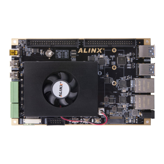
Page 55: Part 3.19: Alinx Customized Fan
Ethernet, USB2.0, SD, DP, CAN, RS485 +1.2V BANK65 of Core Board Part 3.19: ALINX Customized Fan Because AXU5EV-E generates a lot of heat when it works normally, we add a heat sink and fan to the chip on the board to prevent the chip from overheating. -
Page 56: Part 3.20: Carrier Board Size Dimension
The power of the fan is connected to the socket of J24. The red is positive and the black is negative. Part 3.20: Carrier Board Size Dimension Figure 3-20-1: Top View Amazon Store: https://www.amazon.com/alinx 56 / 56...
Need help?
Do you have a question about the ZYNQ UltraScale+ AXU5EV-E and is the answer not in the manual?
Questions and answers