Sign In
Upload
Download
Table of Contents
Contents
Add to my manuals
Delete from my manuals
Share
URL of this page:
HTML Link:
Bookmark this page
Add
Manual will be automatically added to "My Manuals"
Print this page
×
Bookmark added
×
Added to my manuals
Manuals
Brands
Alinx Manuals
Motherboard
AXU2CGA
User manual
Alinx AXU2CGA User Manual
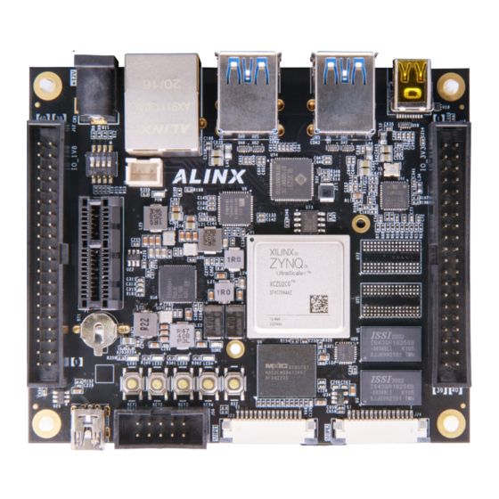
Zynq ultrascale+ fpga development board
Hide thumbs
1
2
Table Of Contents
3
4
5
6
7
8
9
10
11
12
13
14
15
16
17
18
19
20
21
22
23
24
25
26
27
28
29
page
of
29
Go
/
29
Contents
Table of Contents
Bookmarks
Table of Contents
Version Record
Table of Contents
Part 1: AXU2CGA/B Introduction
Part 2: ZYNQ Chip
Part 3: DDR4 DRAM
Part 4: QSPI Flash
Part 5: Emmc Flash (Only for AXU2CGB)
Part 6: EEPROM
Part 7: DP Display Interface
Part 8: USB 3.0 Interface
Part 9: Gigabit Ethernet Interface
Part 10: USB to Serial Port
Part 11: SD Card Slot Interface
Part 12: PCIE Interface
Part 13: 40-Pin Expansion Header
Part 14: MIPI Camera Interface
Part 15: JTAG Debug Port
Part 16: DIP Switch Configuration
Part 17: Leds
Part 18: System Clock
Part 19: ALINX Customized Fan Interface
Part 20: Power Input
Part 21: Board Size Dimension
Advertisement
Quick Links
1
Version Record
2
Part 1: Axu2Cga/B Introduction
3
Part 8: Usb 3.0 Interface
4
Part 12: Pcie Interface
5
Part 14: Mipi Camera Interface
Download this manual
ZYNQ UltraScale+
FPGA Development Board
AXU2CGA/B
User Manual
Table of
Contents
Previous
Page
Next
Page
1
2
3
4
5
Advertisement
Table of Contents
Need help?
Do you have a question about the AXU2CGA and is the answer not in the manual?
Ask a question
Questions and answers
Related Manuals for Alinx AXU2CGA
Motherboard Alinx AXU4EV-E User Manual
Zynq ultrascale+ fpga development board (58 pages)
Motherboard Alinx AXU2CGB User Manual
Zynq ultrascale+ fpga development board (29 pages)
Motherboard Alinx ZYNQ UltraScale+ AXU5EV-E User Manual
Fpga development board (56 pages)
Motherboard Alinx ZYNQ UltraScale+ User Manual
Fpga development board (66 pages)
Motherboard Alinx ZYNQ UltraScale+ User Manual
Fpga development board (66 pages)
Motherboard Alinx AXU7EV User Manual
Zynq ultrascale + fpga board (68 pages)
Motherboard Alinx AXU5EV-P User Manual
Fpga development board (66 pages)
Motherboard Alinx ZYNQ UltraScale+ AXU2CG-E User Manual
Fpga development board (56 pages)
Motherboard Alinx AXU2CGB-E User Manual
Zynq ultrascale+ mpsoc fpga development board (57 pages)
Motherboard Alinx ZYNQ UltraScale+ AXU9EGB User Manual
Fpga development board (66 pages)
Motherboard Alinx ZYNQUltraScale+ AXU3EGB User Manual
Fpga development board (58 pages)
Motherboard Alinx AXU4EVB-E User Manual
Zynq ultrascale+ mpsoc fpga development board (59 pages)
Motherboard Alinx ZYNQ UltraScale+ AXU3EG User Manual
Fpga development board (57 pages)
Motherboard Alinx Cyclone IV FPGA User Manual
(52 pages)
Motherboard Alinx AX7035 User Manual
Xilinx artix-7 fpga (42 pages)
Motherboard Alinx AX7325 User Manual
Kintex-7fpga development board (48 pages)
This manual is also suitable for:
Axu2cgb
Table of Contents
Print
Rename the bookmark
Delete bookmark?
Delete from my manuals?
Login
Sign In
OR
Sign in with Facebook
Sign in with Google
Upload manual
Upload from disk
Upload from URL


Need help?
Do you have a question about the AXU2CGA and is the answer not in the manual?
Questions and answers