Table of Contents
Advertisement
Quick Links
Advertisement
Table of Contents

Related Manuals for Alinx Cyclone IV FPGA


Summary of Contents for Alinx Cyclone IV FPGA
- Page 1 Cyclone IV FPGA Development Board AX515 User Manual...
- Page 2 Cyclone IV FPGA Development Board AX515 User Manual Version Record Version Date Release By Description Rev 1.0 2019-04-30 Rachel Zhou First Release 2 / 52 Contact Email: rachel.zhou@alinx.com.cn...
-
Page 3: Table Of Contents
Cyclone IV FPGA Development Board AX515 User Manual Table of Contents Part 1: FPGA Development Board Introduction .......... 5 Part 2: Structure Diagram ................8 Part 3: Power ....................9 Part 4: FPGA Chip ..................11 Part 4.1: FPGA resources ..........12 Part 4.2: JTAG Interface .......... - Page 4 Cyclone IV FPGA Development Board AX515 User Manual Part 20: 7-segment displays ..............50 4 / 52 Contact Email: rachel.zhou@alinx.com.cn...
-
Page 5: Part 1: Fpga Development Board Introduction
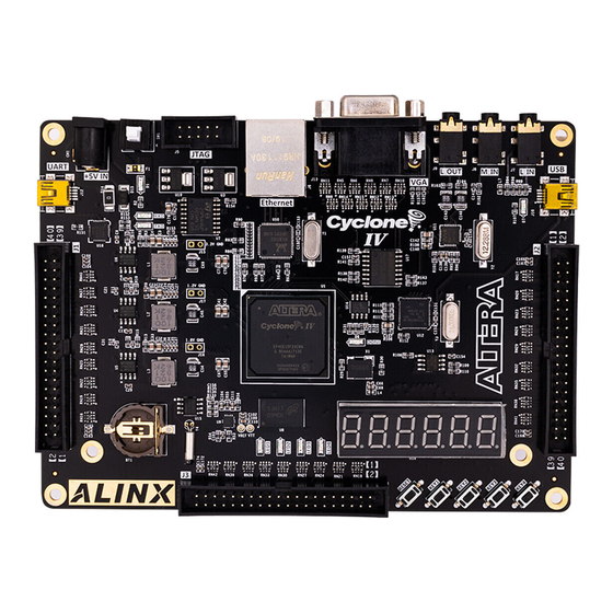
Cyclone IV FPGA Development Board AX515 User Manual The FPGA development board (AX515) is an entry-level product, mainly for FPGA beginners. The FPGA development board uses the ALTERA CYCLONE IV family chips, model EP4CE15F23C8, in a 484-pin FBGA package. The AX515 FPGA development board has a wealth of hardware resources and peripheral interfaces. - Page 6 Cyclone IV FPGA Development Board AX515 User Manual Table 1-1: The Feature Summary of FPGA Device The main resources and features are listed (see Table 1-2): Parameter Value Logic elements (LEs) 15408 Embedded memory (Kbits) Embedded 18 x18 multipliers General-purpose PLLs...
- Page 7 Cyclone IV FPGA Development Board AX515 User Manual 电源 开关 千兆 65535色 音频接口 电源 网口 VGA接口 接口 电源 USB接 指示灯 口 USB转 128Mbit 千兆以太 串口 64Mbit FLASH 网芯片 音频芯片 配置芯片 3.3V电源 EEPROM FPGA 24LC04 1.2V电源 EP4CE15F23C8 USB2.0 芯片 晶振 1.8V电源...
-
Page 8: Part 2: Structure Diagram
On-board 50M active crystal oscillator provides stable clock source for FPGA development board 3-Way 40-pin ALINX expansion port (0.1 inch), each expansion port with 34 IO ports, one 5V power supply, two 3.3V power supplies, three GND. Two expansion modules can be connected at the same time, such as expansion modules such as 4.3-inch TFT module and AD/DA module. -
Page 9: Part 3: Power
Cyclone IV FPGA Development Board AX515 User Manual Figure 2-1: Structure Diagram Part 3: Power The power supply voltage of the AX515 FPGA development board is DC5V, and Figure 3-1 is the power supply schematic: 5V 电源 输入 3.3V/2A FPGA/GPHY... - Page 10 Cyclone IV FPGA Development Board AX515 User Manual The FPGA development board is powered by +5V, and is converted into +3.3V, +1.2V, +1.8V three-way power supply through three-way DC/DC power supply chip MP1482, and generates +2.5V power supply and VCCIO (2.5V) through two LDO LT1117.
-
Page 11: Part 4: Fpga Chip
Cyclone IV FPGA Development Board AX515 User Manual In the PCB design, the 6-layer PCB is used, and a separate power supply layer and GND layer are reserved, so that the power supply of the entire development board has very good stability. Test points for each power supply are reserved on the PCB so that the user can confirm the voltage on the board. -
Page 12: Part 4.1: Fpga Resources
Cyclone IV FPGA Development Board AX515 User Manual Part 4.1: FPGA Resources The EP4CE15F23C8 chip contains logic resources, built-in RAM, multiplier, phase-locked loop, global clock network and IO port. The resources between different types of FPGAs will be different. The resources of the FPGA model on the AX515 development board are shown in Figure 3-2 below Figure 4-2:FPGA internal resources... -
Page 13: Part 4.3: Fpga Power Supply
Cyclone IV FPGA Development Board AX515 User Manual signals TCK, TDO, TMS, TDI. Figure 4-3: JTAGE Schematic The JTAG interface uses a 10-pin 2.54mm standard connector, and Figure 3-4 shows the JTAG interface on the FPGA development board. Figure 4-4: JTAG Connector on the FPGA board Part 4.3: FPGA Power Supply... -
Page 14: Part 5: 50Mhz Clock
Cyclone IV FPGA Development Board AX515 User Manual can choose the voltage according to our own needs, the default is 3.3V. Change the resistance of R158 to R159 and change the BANK7 voltage to 2.5V. If there are other requirements, different voltages can be achieved by replacing the power supply chip U19. -
Page 15: Part 6: Spi Flash Configuration Chip
Cyclone IV FPGA Development Board AX515 User Manual Figure 5-1: 50Mhz Crystal Oscillator Figure 5-2: 50Mhz crystal oscillator on the FPGA Development Board Clock Pin Assignment Net Name FPGA PIN Part 6: SPI Flash Configuration chip A 64Mbit configuration chip is used on the development board, the model is M25P64. - Page 16 Cyclone IV FPGA Development Board AX515 User Manual Due to its non-volatile nature, the configuration chip can be used as a storage device for storing configuration information of the FPGA system during use, and can also save information content when power is off. When power is restored, the configuration chip EPCS64 transfers the configuration information to the FPGA and then runs.
-
Page 17: Part 7: Qspi Flash
Cyclone IV FPGA Development Board AX515 User Manual Figure 6-2: EPCS64(M25P64) on the FPGA board Configure chip pin assignments: Pin Name FPGA Pin ASDO DCLK nCSO DATA0 Part 7: QSPI Flash The AX515 FPGA development board is equipped with a 128MBit Quad-SPI FLASH chip, model W25Q128, which uses the 3.3V CMOS voltage... - Page 18 Cyclone IV FPGA Development Board AX515 User Manual parameters of QSPI FLASH are shown in Table 7-1. Position Model Capacity Factory W25Q128BV 128M Bit Winbond Table 7-1: QSPI FLASH Specification Figure 7-1: QSPI Flash Schematic 18 / 52 Contact Email: rachel.zhou@alinx.com.cn...
-
Page 19: Part 8: Ddr2 Dram
Cyclone IV FPGA Development Board AX515 User Manual Figure 7-2: QSPI Flash chip on the FPGA board Configure chip pin assignments: Pin Name FPGA Pin QSPI_CLK QSPI_CS QSPI_MISO0 QSPI_MISO1 QSPI_MISO2 QSPI_MISO3 Part 8: DDR2 DRAM The development board contains a high-speed DDR2 DRAM, model: MT47H64M16HR-3IT, capacity: 1Gbit (64M*16bit), 16bit bus. - Page 20 Cyclone IV FPGA Development Board AX515 User Manual DDR2 is up to 166.7MHz, and the data frequency is up to 333MHz. The hardware design of DDR2 requires strict consideration of signal integrity. In the circuit design and PCB design, the matching resistor/terminal resistor, trace impedance control, and trace length control have been fully considered to ensure the high-speed stability of DDR2.
- Page 21 Cyclone IV FPGA Development Board AX515 User Manual Figure 8-2: DDR2 DRAM on the FPGA Board DDR2 DRAM Pin Assignment: Pin Name FPGA Pin DDR2_DQS[0] DDR2_DQS[1] DDR2_DQ[0] DDR2_DQ [1] DDR2_DQ [2] DDR2_DQ [3] DDR2_DQ [4] DDR2_DQ [5] DDR2_DQ [6] DDR2_DQ [7]...
- Page 22 Cyclone IV FPGA Development Board AX515 User Manual DDR2_DQ [12] DDR2_DQ [13] DDR2_DQ [14] DDR2_DQ [15] DDR2_DM[1] DDR2_DM[0] DDR2_A[0] DDR2_A [1] DDR2_A [2] DDR2_A [3] DDR2_A [4] DDR2_A [5] DDR2_A [6] DDR2_A [7] DDR2_A [8] DDR2_A [9] DDR2_A [10] DDR2_A [11]...
-
Page 23: Part 9: Eeprom 24Lc04
Cyclone IV FPGA Development Board AX515 User Manual Part 9: EEPROM 24LC04 The development board contains an EEPROM, model 24LC04, and its capacity is 4Kbit (2*256*8bit). It consists of two 256-byte blocks and communicates via the IIC bus. The onboard EEPROM is to learn the communication method of the IIC bus. -
Page 24: Part 10:Real-Time Clock
Cyclone IV FPGA Development Board AX515 User Manual Figure 9-2: EEPROM on the AX515 FPGA board EEPROM PIN assignment: Net Name FPGA PIN EEPROM_I2C_SDA EEPROM_I2C_SCL Part 10:Real-Time Clock DS1302 The FPGA development board contains a real-time clock RTC chip, model DS1302. - Page 25 Cyclone IV FPGA Development Board AX515 User Manual powered or not, the DS1302 will operate normally without interruption and provide continuous time information. Figure 10-1 shows the schematic of the DS1302: Figure 10-1 RTC Hardware Design Figure 10-2: DS1302 Circuit on FPGA board 25 / 52 Contact Email: rachel.zhou@alinx.com.cn...
-
Page 26: Part 11: Gigabit Ethernet Interface
Cyclone IV FPGA Development Board AX515 User Manual DS1302 Interface Pin Assignment: Net Name FPGA PIN RTC_SIO RTC_RESET RTC_SCLK Part 11: Gigabit Ethernet Interface The AX515 FPGA development board provides network communication services to users through the Realtek RTL8211EG Ethernet PHY chip. The RTL8211EG chip supports 10/100/1000 Mbps network transmission rate and communicates with the FPGA through the GMII interface. - Page 27 Cyclone IV FPGA Development Board AX515 User Manual transmission clock is 125Mhz. The receive clock E_RXC is provided by the PHY chip, the transmit clock E_GTXC is provided by the FPGA, and the data is sampled on the rising edge of the clock.
- Page 28 Cyclone IV FPGA Development Board AX515 User Manual Gigabit Ethernet pin assignments are as follows: Signal Name FPGA Pin Description Ethernet GMII transmit clock E_GCLK Ethernet Transmit Data bit0 E_TXD0 Ethernet Transmit Data bit1 E_TXD1 Ethernet Transmit Data bit2 E_TXD2...
-
Page 29: Part 12: Usb To Serial Port
Cyclone IV FPGA Development Board AX515 User Manual Part 12: USB to Serial Port The AX515 FPGA development board includes the USB-UAR chip of Silicon Labs CP2102GM. The USB interface uses the MINI USB interface. It can be connected to the USB port of the upper PC for serial data communication with a USB cable. - Page 30 Cyclone IV FPGA Development Board AX515 User Manual At the same time, two LED indicators LED7 (RXD) and LED8 (TXD) are set for the serial port signal, and the silkscreen on the PCB is TX and RX, indicating that the serial port has data transmission or reception, as shown in the following...
-
Page 31: Part 13: Vga Port
Cyclone IV FPGA Development Board AX515 User Manual Part 13: VGA Port VGA interface, I believe many friends will not be unfamiliar, because this interface is the most important interface on the computer monitor. From the era of huge CRT monitors, the VGA interface has been used, and it has been used until now, and the VGA interface is also called For the D-Sub interface. - Page 32 Cyclone IV FPGA Development Board AX515 User Manual interface hardware design. Figure 13-2: VGA Interface Hardware Design Figure 13-3: VGA Interface on board VGA Interface Pin Assignment Pin Name FPGA Pin Description BLUE[0] VGA_B[0] BLUE[1] VGA_B[1] BLUE[2] VGA_B[2] BLUE[3] VGA_B[3]...
-
Page 33: Part 14: Usb 2.0 Interface
Cyclone IV FPGA Development Board AX515 User Manual GREEN[2] VGA_G[2] GREEN[3] VGA_G[3] GREEN[4] VGA_G[4] GREEN[5] VGA_G[5] RED[0] VGA_R[0] RED[1] VGA_R[1] RED[2] VGA_R[2] RED[3] VGA_R[3] RED[4] VGA_R[4] Horizontal sync signal VGA_HS Vertical sync signal VGA_VS Part 14: USB 2.0 interface The FPGA development board uses Cypress CY7C68013A USB2.0 controller chip to realize high-speed data communication between PC and FPGA. - Page 34 Cyclone IV FPGA Development Board AX515 User Manual Figure 14-1: FPGA and CY7C68013A connection diagram Figure 14-2 is a USB2.0 interface schematic, U12 is CY7C68013A, J10 is a USB interface. Figure 14-2: USB2.0 interface on the FPGA Board 34 / 52...
- Page 35 Cyclone IV FPGA Development Board AX515 User Manual USB2.0 Pin Assignment: Pin Name FPGA Pin Description 12-, 24- or 48 MHz clock output USB_CLKOUT Synchronous Communication Clock USB_IFCLK Signal Status Output Signal USB_FLAGA Status Output Signal USB_FLAGB Status Output Signal...
-
Page 36: Part 15: Audio Interface
Cyclone IV FPGA Development Board AX515 User Manual Part 15: Audio Interface The AX515 development board uses the Wolfon WM8731 audio codec (CODEC) chip to provide users with a high-quality audio interface. The chip supports microphone input, line input and line output port, and the sampling rate is adjustable from 8kHz to 96kHz. -
Page 37: Part 16: Sd Card Slot
Cyclone IV FPGA Development Board AX515 User Manual Figure 15-2: Audio interface on the FPGA board Audio WM8731 Pin Assignment: Pin Name FPGA Pin Description VM_I2C_SCLK WM8731 IIC Clock VM_I2C_SDAT WM8731 IIC Clock VM_BCLK Audio data clock signal Audio data output... - Page 38 Cyclone IV FPGA Development Board AX515 User Manual the United States conducted substantial research and development. In 2000, these companies initiated the establishment of the SD Association (Secure Digital Association, SDA), which has a strong lineup and attracted a large number of manufacturers.
-
Page 39: Part 17: Expansion Header
Cyclone IV FPGA Development Board AX515 User Manual Figure 16-2: SD Cart Slot on AX515 FPGA Board SD Card Slot Pin Assignment SD Mode FPGA Pin Pin name SD_CLK SD_CMD SD_DAT0 SD_DAT1 SD_DAT2 SD_DAT3 Part 17: Expansion Header The AX515 FPGA development board is reserved with three 0.1inch spacing standard 40-pin expansion headers J1, J2, J3. -
Page 40: Part 17.1: Expansion Header J1
Cyclone IV FPGA Development Board AX515 User Manual supply, 3-channle ground and 34 IOs. Do not directly connect the IO directly to the 5V device to avoid burning the FPGA. If you want to connect 5V equipment, you need to connect level conversion chip. - Page 41 Cyclone IV FPGA Development Board AX515 User Manual Figure 17-2: Expansion header J1 on the FPGA Board J1 Expansion Header Pin Assignment Pin Number FPGA Pin Pin Number FPGA Pin VCC5V 41 / 52 Contact Email: rachel.zhou@alinx.com.cn...
-
Page 42: Part 17.2: Expansion Header J2
Cyclone IV FPGA Development Board AX515 User Manual VCC3V3 VCC3V3 Part 17.2: Expansion header J2 Figure 17-3 shows the J2 expansion port connection diagram. Pin1, Pin37, Pin38 are GND, Pin2 is +5V, and Pin39 and Pin40 are +3.3V. In addition to Pin33 and Pin34, the signals of J2 are connected to the Bank7 of the FPGA in differential pairs. - Page 43 Cyclone IV FPGA Development Board AX515 User Manual Figure 17-4 shows the differential trace of the J2 expansion port PCB. The differential line implements strict isometric, equidistant and impedance 100 ohm control. Figure 17-4: J2 expansion port PCB trace The IO port of the J2 expansion port is connected FPGA Bank7, and the default level is 3.3V.
- Page 44 Cyclone IV FPGA Development Board AX515 User Manual Figure 17-5: Power supply of J2 expansion port Figure 17-6: J2 expansion port on the FPGA Board 44 / 52 Contact Email: rachel.zhou@alinx.com.cn...
- Page 45 Cyclone IV FPGA Development Board AX515 User Manual J2 Expansion Header Pin Assignment Pin Number FPGA Pin Pin Number FPGA Pin VCC5V VCC3V3 VCC3V3 VCC3V3 VCC3V3 45 / 52 Contact Email: rachel.zhou@alinx.com.cn...
-
Page 46: Part 17.3: Expansion Header J3
Cyclone IV FPGA Development Board AX515 User Manual Part 17.3: Expansion header J3 Figure 17-7: Expansion header J3 schematic Figure 17-8: Expansion header J3 on the FPGA Board 46 / 52 Contact Email: rachel.zhou@alinx.com.cn... -
Page 47: Part 18: Led
Cyclone IV FPGA Development Board AX515 User Manual J3 Expansion Header Pin Assignment Pin Name FPGA Pin Pin Name FPGA Pin VCC5V VCC3V3 VCC3V3 Part 18: LED There are six red LEDs on the AX515 FPGA development board, one of which is the power indicator (PWR), four are users LED lights (LED1~LED4). -
Page 48: Part 19: Buttons
Cyclone IV FPGA Development Board AX515 User Manual Figure 18-1: User LEDs Schematic Figure 18-2: User LEDs on the FPGA Board User LEDs Pin Assignment: Pin Name FPGA Pin LED1 LED2 LED3 LED4 Part 19: Keys The AX515 FPGA development board has five independent buttons, 48 / 52 Contact Email: rachel.zhou@alinx.com.cn... - Page 49 Cyclone IV FPGA Development Board AX515 User Manual including four user buttons (KEY1~KEY4) and one reset button RESET. The buttons are active low, and the schematic diagram of the four user buttons is shown in Figure 19-1 Figure 19-1: Four User Button Schematic The reset button is connected to the normal IO of FPGA for reset FPGA program.
- Page 50 Cyclone IV FPGA Development Board AX515 User Manual Keys Pin Assignment Button Name FPGA Pin Key name KEY 1 KEY1 KEY 2 KEY2 KEY 3 KEY3 KEY 4 KEY4 RESET RESET Part 20: 7-segment displays The digital tube is a very common display device. It is generally divided into a seven-segment digital tube and an eight-segment digital tube.
- Page 51 Cyclone IV FPGA Development Board AX515 User Manual The six-in-one digital tube is a dynamic display. Due to the persistence of human vision and the afterglow effect of the LED, although the digital tubes are not lit at the same time, as long as the scanning speed is fast enough, the impression is a group, stable display data, no flickering.
- Page 52 Cyclone IV FPGA Development Board AX515 User Manual Figure 20-3: 7-segment displays on the FPGA board 7-segment displays Pin Assignments: Pin Name FPGA Pin Description Corresponding segment DP SMG_Data[7] Corresponding segment G SMG_Data[6] Corresponding segment F SMG_Data[5] Corresponding segment E...
Need help?
Do you have a question about the Cyclone IV FPGA and is the answer not in the manual?
Questions and answers