Table of Contents
Advertisement
Quick Links
www.dalsemi.com
FEATURES
Complete E1 (CEPT) PCM-30/ISDN-PRI
transceiver functionality
Onboard long and short haul line interface
for clock/data recovery and waveshaping
32-bit or 128-bit crystal-less jitter attenuator
Frames to FAS, CAS, CCS, and CRC4
formats
Integral HDLC controller with 64-byte
buffers configurable for Sa Bits, DS0 or sub
DS0 operation
Dual two–frame elastic store slip buffers that
can connect to asynchronous backplanes up
to 8.192 MHz
Interleaving PCM Bus Operation
8–bit parallel control port that can be used
directly on either multiplexed or non–
multiplexed buses (Intel or Motorola)
Extracts and inserts CAS signaling
Detects and generates remote and AIS alarms
Programmable output clocks for Fractional
E1, H0, and H12 applications
Fully independent transmit and receive
functionality
Full access to Si and Sa bits aligned with
CRC-4 multiframe
Four separate loopback functions for testing
functions
DESCRIPTION
The DS21354/554 Single–Chip Transceiver (SCT) contains all of the necessary functions for connection to E1
lines. The device is an upward compatible version of the DS2153 and DS2154 SCTs. The onboard clock/data
recovery circuitry coverts the AMI/HDB3 E1 waveforms to an NRZ serial stream. The DS21354/554
automatically adjusts to E1 22AWG (0.6 mm) twisted–pair cables from 0 to over 2km in length. The device can
generate the necessary G.703 waveshapes for both 75 ohm coax and 120 ohm twisted cables. The onboard jitter
attenuator (selectable to either 32 bits or 128 bits) can be placed in either the transmit or receive data paths. The
framer locates the frame and multiframe boundaries and monitors the data stream for alarms. It is also used for
extracting and inserting signaling data, Si, and Sa bit information. The onboard HDLC controller can be used
for Sa bit links or DS0s. The device contains a set of internal registers which the user can access and control
the operation of the unit. Quick access via the parallel control port allows a single controller to handle many E1
lines. The device fully meets all of the latest E1 specifications including ITU-T G.703,G.704, G.706, G.823,
G.732, and I.431, ETS 300 011, 300 233, and 300 166, as well as CTR12 and CTR4.
DS21354 (3.3V) and DS21554 (5V)
E1 Single Chip Transceivers (SCT)
Large counters for bipolar and code
violations, CRC4 code word errors, FAS
word errors, and E bits
IEEE 1149.1 JTAG-Boundary Scan
Architecture
Pin compatible with DS2154/52/352/552 SCTs
3.3V (DS21354) or 5V (DS21554) supply;
low power CMOS
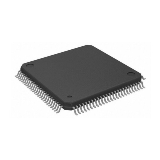
100–pin LQFP package (14mm X 14mm)
100
ORDERING INFORMATION
DS21354L
DS21354LN (-40
DS21554L
DS21554LN (-40
1 of 117
1
0
0
(0
C to 70
C)
0
0
C to +85
C)
0
0
(0
C to 70
C)
0
0
C to +85
C)
020100
Advertisement
Table of Contents

Related Manuals for Dallas Semiconductor DS21354L


Summary of Contents for Dallas Semiconductor DS21354L
- Page 1 Detects and generates remote and AIS alarms Programmable output clocks for Fractional E1, H0, and H12 applications Fully independent transmit and receive ORDERING INFORMATION functionality DS21354L C to 70 Full access to Si and Sa bits aligned with DS21354LN (-40 C to +85 CRC-4 multiframe...
-
Page 2: Table Of Contents
DS21354 & DS21554 TABLE OF CONTENTS LIST OF FIGURES ........................5 LIST OF TABLES ........................6 INTRODUCTION......................... 7 Functional Description ......................8 Document Revision History...................... 9 PIN DESCRIPTION ........................11 Pin Function Description ......................15 4.1.1 Transmit Side Pins......................15 4.1.2 Receive Side Pins ...................... - Page 3 DS21354 & DS21554 SIGNALING OPERATION....................... 48 10.1 Processor Based Signaling ......................48 10.2 Hardware Based Signaling...................... 51 10.2.1 Receive Side ........................51 10.2.2 Transmit Side......................... 51 PER-CHANNEL CODE GENERATION AND LOOPBACK..........52 11.1 Transmit Side Code Generation....................52 11.1.1 Simple Idle Code Insertion and Per-Channel Loopback ..........52 11.1.2 Per-Channel Code Insertion ..................
- Page 4 DS21354 & DS21554 INTERLEAVED PCM BUS OPERATION ................86 18.1 Channel Interleave ........................87 18.2 Frame Interleave........................87 FUNCTIONAL TIMING DIAGRAMS ..................88 19.1 Receive............................ 88 19.2 Transmit ..........................94 OPERATING PARAMETERS ....................103 AC TIMING PARAMETERS AND DIAGRAMS ..............104 21.1 Multiplexed Bus AC Characteristics..................
-
Page 5: List Of Figures
DS21354 & DS21554 1 LIST OF FIGURES Figure 3-1 DS2135/554 BLOCK DIAGRAM ................10 Figure 16-1 BASIC EXTERNAL ANALOG CONNECTIONS ............71 Figure 16-2 OPTIONAL CRYSTAL CONNECTION..............72 Figure 16-3 JITTER TOLERANCE ....................72 Figure 16-4 JITTER ATTENUATION..................... 73 Figure 16-5 TRANSMIT WAVEFORM TEMPLATE .............. -
Page 6: List Of Tables
DS21354 & DS21554 2 LIST OF TABLES Table 4-1 PIN DESCRIPTION SORTED BY PIN NUMBER ............. 11 Table 4-2 PIN DESCRIPTION BY SYMBOL ................13 Table 5-1 REGISTER MAP SORTED BY ADDRESS ..............25 Table 6-1 DEVICE ID BIT MAP ....................29 Table 6-2 SYNC/RESYNC CRITERIA .................. -
Page 7: Introduction
DS21354 & DS21554 3 INTRODUCTION The DS21354/554 is a superset version of the popular DS2153 and DS2154 SCTs offering the new features listed below. All of the original features of the DS2153 and DS2154 have been retained and software created for the original devices is transferable into the DS21354/554. New Features in the DS21354 and DS21554 FEATURE SECTION... -
Page 8: Functional Description
DS21354 & DS21554 3.1 Functional Description The analog AMI/HDB3 waveform off of the E1 line is transformer coupled into the RRING and RTIP pins of the DS21354/554. The device recovers clock and data from the analog signal and passes it through the jitter attenuation mux to the receive side framer where the digital serial stream is analyzed to locate the framing/multi-frame pattern. -
Page 9: Document Revision History
DS21354 & DS21554 3.2 DOCUMENT REVISION HISTORY Date Notes 1-27-99 Initial release 1-28-99 Corrected TSYSCLK and RSYSCLK timing and added 4.096 MHz and 8.192 MHz timing 2-3-99 Corrected definition and label of TUDR bit in the THIR register. 2-11-99 Correct address of IBO register in text. 4-1-99 Add Receive Monitor Mode section 4-15-99... - Page 10 RCLK RLOS/LOTC 8.192MHz Clock HDLC/BOC 8MCLK Synthesizer Controller RLINK Sa / DS0 RLCLK LIUC RCHBLK RCHCLK VCO / PLL RSIGF Timing RSIG Signaling Receive Side Control 32.768MHz RSER Buffer Framer RSYSCLK DATA Interleave RRING RSYSCLK Elastic CLOCK Store RSYNC RTIP SYNC RMSYNC RFSYNC...
-
Page 11: Pin Description
DS21354 & DS21554 4 PIN DESCRIPTION PIN DESCRIPTION SORTED BY PIN NUMBER Table 4-1 SYMBOL TYPE DESCRIPTION RCHBLK Receive Channel Block JTMS IEEE 1149.1 Test Mode Select 8MCLK 8.192 MHz Clock JTCLK IEEE 1149.1 Test Clock Signal JTRST* IEEE 1149.1 Test Reset Receive Carrier Loss JTDI IEEE 1149.1 Test Data Input... - Page 12 DS21354 & DS21554 SYMBOL TYPE DESCRIPTION DVDD – Digital Positive Supply DVSS – Digital Signal Ground TCLK Transmit Clock TSER Transmit Serial Data TSIG Transmit Signaling Input TESO Transmit Elastic Store Output TDATA Transmit Data TSYSCLK Transmit System Clock TSSYNC Transmit System Sync TCHCLK Transmit Channel Clock...
- Page 13 DS21354 & DS21554 SYMBOL TYPE DESCRIPTION RNEGO Receive Negative Data Output RPOSO Receive Positive Data Output RCHCLK Receive Channel Clock RSIGF Receive Signaling Freeze Output RSIG Receive Signaling Output RSER Receive Serial Data RMSYNC Receive Multiframe Sync RFSYNC Receive Frame Sync RSYNC Receive Sync RLOS/LOTC...
- Page 14 DS21354 & DS21554 SYMBOL TYPE DESCRIPTION JTCLK IEEE 1149.1 Test Clock Signal JTDI IEEE 1149.1 Test Data Input JTDO IEEE 1149.1 Test Data Output JTMS IEEE 1149.1 Test Mode Select JTRST* IEEE 1149.1 Test Reset LIUC Line Interface Connect MCLK Master Clock Input Bus Operation –...
-
Page 15: Pin Function Description
DS21354 & DS21554 SYMBOL TYPE DESCRIPTION TCLKI Transmit Clock Input TCLKO Transmit Clock Output TDATA Transmit Data TESO Transmit Elastic Store Output TEST Test TLCLK Transmit Link Clock TLINK Transmit Link Data TNEGI Transmit Negative Data Input TNEGO Transmit Negative Data Output TPOSI Transmit Positive Data Input TPOSO... - Page 16 DS21354 & DS21554 Signal Name: TCHBLK Signal Description: Transmit Channel Block Signal Type: Output A user programmable output that can be forced high or low during any of the 32 E1 channels. Synchronous with TCLK when the transmit side elastic store is disabled. Synchronous with TSYSCLK when the transmit side elastic store is enabled.
- Page 17 DS21354 & DS21554 Signal Name: TESO Signal Description: Transmit Elastic Store Data Output Signal Type: Output Updated on the rising edge of TCLK with data out of the transmit side elastic store whether the elastic store is enabled or not. This pin is normally tied to TDATA. Signal Name: TDATA Signal Description:...
-
Page 18: Receive Side Pins
DS21354 & DS21554 4.1.2 Receive Side Pins Signal Name: RLINK Signal Description: Receive Link Data Signal Type: Output Updated with the full recovered E1 data stream on the rising edge of RCLK. Signal Name: RLCLK Signal Description: Receive Link Clock Signal Type: Output 4 kHz to 20 kHz clock (Sa bits) for the RLINK output. - Page 19 DS21354 & DS21554 Signal Name: RFSYNC Signal Description: Receive Frame Sync Signal Type: Output An extracted 8 kHz pulse, one RCLK wide, is output at this pin which identifies frame boundaries. Signal Name: RMSYNC Signal Description: Receive Multiframe Sync Signal Type: Output If the receive side elastic store is enabled, an extracted pulse, one RSYSCLK wide, is output at this pin which identifies multiframe boundaries.
-
Page 20: Parallel Control Port Pins
DS21354 & DS21554 Signal Name: 8MCLK Signal Description: 8 MHz Clock Signal Type: Output An 8.192MHz clock output that is referenced to the clock that is output at the RCLK pin. Signal Name: RPOSO Signal Description: Receive Positive Data Input Signal Type: Output Updated on the rising edge of RCLKO with bipolar data out of the line interface. - Page 21 DS21354 & DS21554 Signal Name: Signal Description: Framer Mode Select Signal Type: Input Selects the DS2154 mode when high or the DS21354/554 mode when low. If high, the JTRST* is internally pulled low. If low, JTRST* has normal JTAG functionality. This pin has a 10k pull up resistor.
-
Page 22: Jtag Test Access Port Pins
DS21354 & DS21554 Signal Name: ALE(AS)/a7 Signal Description: Address Latch Enable(Address Strobe) or A7 Signal Type: Input In non–multiplexed bus operation (MUX = 0), serves as the upper address bit. In multiplexed bus operation (MUX = 1), serves to de-multiplex the bus on a positive–going edge. Signal Name: WR*(R/W*) Signal Description:... -
Page 23: Interleave Bus Operation Pins
DS21354 & DS21554 4.1.5 Interleave Bus Operation Pins Signal Name: Signal Description: Carry In Signal Type: Input A rising edge on this pin causes RSER and RSIG to come out of high Z state and TSER and TSIG to start sampling on the next rising edge of RSYSCLK/TSYSCLK beginning an I/O sequence of 8 or 256 bits of data. -
Page 24: Supply Pins
DS21354 & DS21554 Signal Name: TTIP & TRING Signal Description: Transmit Tip and Ring Signal Type: Output Analog line driver outputs. These pins connect via a step–up transformer to the E1 line. See Section 0 for details. 4.1.7 Supply Pins Signal Name: DVDD Signal Description:... -
Page 25: Register Map
DS21354 & DS21554 5.1 REGISTER MAP REGISTER MAP SORTED BY ADDRESS Table 5-1 ADDRESS REGISTER NAME REGISTER ABBREVIATION BPV or Code Violation Count 1 VCR1 BPV or Code Violation Count 2 VCR2 CRC4 Error Count 1 / FAS Error Count 1 CRCCR1 CRC4 Error Count 2 CRCCR2... - Page 26 DS21354 & DS21554 ADDRESS REGISTER NAME REGISTER ABBREVIATION Transmit Idle Definition TIDR Receive Channel Blocking 1 RCBR1 Receive Channel Blocking 2 RCBR2 Receive Channel Blocking 3 RCBR3 Receive Channel Blocking 4 RCBR4 Receive Align Frame Receive Signaling 1 Receive Signaling 2 Receive Signaling 3 Receive Signaling 4 Receive Signaling 5...
- Page 27 DS21354 & DS21554 ADDRESS REGISTER NAME REGISTER ABBREVIATION Transmit Sa8 Bits TSa8 Receive Si bits Align Frame RSiAF Receive Si bits Non-Align Frame RSiNAF Receive Remote Alarm Bits Receive Sa4 Bits RSa4 Receive Sa5 Bits RSa5 Receive Sa6 Bits RSa6 Receive Sa7 Bits RSa7 Receive Sa8 Bits...
- Page 28 DS21354 & DS21554 ADDRESS REGISTER NAME REGISTER ABBREVIATION Receive Channel 5 Receive Channel 6 Receive Channel 7 Receive Channel 8 Receive Channel 9 Receive Channel 10 RC10 Receive Channel 11 RC11 Receive Channel 12 RC12 Receive Channel 13 RC13 Receive Channel 14 RC14 Receive Channel 15 RC15...
-
Page 29: Control, Id, And Test Registers
DS21354 & DS21554 ADDRESS REGISTER NAME REGISTER ABBREVIATION HDLC Status Register HDLC Interrupt Mask Register HIMR Receive HDLC Information Register RHIR Receive HDLC FIFO Register RHFR Interleave Bus Operation Register Transmit HDLC Information Register THIR Transmit HDLC FIFO Register THFR Receive HDLC DS0 Control Register 1 RDC1 Receive HDLC DS0 Control Register 2... -
Page 30: Power-Up Sequence
DS21354 & DS21554 The Test registers at addresses 09, 15, 19, and AC hex are used by the factory in testing the DS21354/554. On power-up, the Test registers should be set to 00h in order for the DS21354/554 to operate properly. 6.1 Power–Up Sequence On power–up, after the supplies are stable the DS21354/554 should be configured for operation by writing to all of the internal registers (this includes setting the Test Registers to 00h) since the contents of... -
Page 31: Synchronizatrion And Re-Synchronization
DS21354 & DS21554 SYMBOL POSITION NAME AND DESCRIPTION – RCR1.3 Not Assigned. Should be set to zero when written. RCR1.2 Frame Resync Criteria. 0 = resync if FAS received in error 3 consecutive times 1 = resync if FAS or bit 2 of non–FAS is received in error 3 consecutive times SYNCE RCR1.1... - Page 32 DS21354 & DS21554 RCR2: RECEIVE CONTROL REGISTER 2 (Address=11 Hex) (MSB) (LSB) Sa8S Sa7S Sa6S Sa5S Sa4S RBCS RESE – SYMBOL POSITION NAME AND DESCRIPTION Sa8S RCR2.7 Sa8 Bit Select. Set to one to have RLCLK pulse at the Sa8 bit position; set to zero to force RLCLK low during Sa8 bit position.
- Page 33 DS21354 & DS21554 SYMBOL POSITION NAME AND DESCRIPTION TSiS TCR1.3 Transmit International Bit Select. 0 = sample Si bits at TSER pin 1 = source Si bits from TAF and TNAF registers (in this mode, TCR1.6 must be set to 0) TSA1 TCR1.2 Transmit Signaling All Ones.
-
Page 34: Framer Loopback
DS21354 & DS21554 CCR1: COMMON CONTROL REGISTER 1 (Address=14 Hex) (MSB) (LSB) THDB3 TG802 TCRC4 RHDB3 RG802 RCRC4 SYMBOL POSITION NAME AND DESCRIPTION CCR1.7 Framer Loopback. 0 = loopback disabled 1 = loopback enabled THDB3 CCR1.6 Transmit HDB3 Enable. 0 = HDB3 disabled 1 = HDB3 enabled TG802 CCR1.5... -
Page 35: Automatic Alarm Generation
DS21354 & DS21554 CCR2: COMMON CONTROL REGISTER 2 (Address=1A Hex) (MSB) (LSB) ECUS VCRFS AAIS RSERC LOTCMC SYMBOL POSITION NAME AND DESCRIPTION ECUS CCR2.7 Error Counter Update Select. See Section 8 for details. 0 = update error counters once a second 1 = update error counters every 62.5 ms (500 frames) VCRFS CCR2.6... - Page 36 DS21354 & DS21554 RAI generation conforms to ETS 300 011 specifications and a constant Remote Alarm will be transmitted if the DS21354/554 cannot find CRC4 multiframe synchronization within 400 ms as per G.706. CCR3: COMMON CONTROL REGISTER 3 (Address=1B Hex) (MSB) (LSB) TESE...
-
Page 37: Remote Loopback
DS21354 & DS21554 SYMBOL POSITION NAME AND DESCRIPTION CCR4.6 Local Loopback. 0 = loopback disabled 1 = loopback enabled LIAIS CCR4.5 Line Interface AIS Generation Enable. 0 = allow normal data from TPOSI/TNEGI to be transmitted at TTIP and TRING 1 = force unframed all ones to be transmitted at TTIP and TRING at the MCLK rate TCM4... - Page 38 DS21354 & DS21554 SYMBOL POSITION NAME AND DESCRIPTION Should be toggled after RSYSCLK has been applied and is stable. Must be cleared and set again for a subsequent align. See Section 13 for details. TESA CCR5.5 Transmit Elastic Store Align. Setting this bit from a zero to a one may force the transmit elastic store’s write/read pointers to a minim separation of half a frame.
-
Page 39: Status And Information Registers
DS21354 & DS21554 SYMBOL POSITION NAME AND DESCRIPTION – CCR6.4 Not Assigned. Should be set to zero when written. – CCR6.3 Not Assigned. Should be set to zero when written. TCLKSRC CCR6.2 Transmit Clock Source Select. This function allows the user to internally select RCLK as the clock source for the transmit side formatter. - Page 40 DS21354 & DS21554 The SR1, SR2, and HSR registers have the unique ability to initiate a hardware interrupt via the INT* output pin. Each of the alarms and events in the SR1, SR2, and HSR can be either masked or unmasked from the interrupt pin via the Interrupt Mask Register 1 (IMR1), Interrupt Mask Register 2 (IMR2), and HDLC Interrupt Mask Register (HIMR) respectively.
-
Page 41: Crc4 Sync Counter
DS21354 & DS21554 SSR: SYNCHRONIZER STATUS REGISTER (Address=1E Hex) (MSB) (LSB) CSC5 CSC4 CSC3 CSC2 CSC0 FASSA CASSA CRC4SA SYMBOL POSITION NAME AND DESCRIPTION CSC5 SSR.7 CRC4 Sync Counter Bit 5. MSB of the 6–bit counter. CSC4 SSR.6 CRC4 Sync Counter Bit 4. CSC3 SSR.5 CRC4 Sync Counter Bit 3. - Page 42 DS21354 & DS21554 SYMBOL POSITION NAME AND DESCRIPTION SR1.1 Receive Carrier Loss. Set when 255 (or 2048 if CCR3.0=1) consecutive zeros have been detected at RTIP and RRING. (note: a receiver carrier loss based on data received at RPOSI and RNEGI is available in the HSR register) RLOS SR1.0...
- Page 43 DS21354 & DS21554 SYMBOL POSITION NAME AND DESCRIPTION SR2.3 Transmit Align Frame. Set every 250 ns at the beginning of align frames. Used to alert the host that the TAF and TNAF registers need to be updated. LOTC SR2.2 Loss of Transmit Clock. Set when the TCLK pin has not transitioned for one channel time (or 3.9 ns).
-
Page 44: Error Count Registers
DS21354 & DS21554 IMR2: INTERRUPT MASK REGISTER 2 (Address=17 Hex) (MSB) (LSB) LOTC RCMF TSLIP SYMBOL POSITION NAME AND DESCRIPTION IMR2.7 Receive CAS Multiframe. 0 = interrupt masked 1 = interrupt enabled IMR2.6 Receive Align Frame. 0 = interrupt masked 1 = interrupt enabled IMR2.5 Transmit Multiframe. -
Page 45: Crc4 Error Counter
DS21354 & DS21554 In most applications, the framer should be programmed to count BPVs when receiving AMI code and to count CVs when receiving HDB3 code. This counter increments at all times and is not disabled by loss of sync conditions. The counter saturates at 65,535 and will not rollover. The bit error rate on an E1 line would have to be greater than 10**–2 before the VCR would saturate. -
Page 46: Fas Error Counter
DS21354 & DS21554 EBCR1: E–BIT COUNT REGISTER 1 (Address=04 Hex) EBCR2: E–BIT COUNT REGISTER 2 (Address=05 Hex) (MSB) (LSB) (note 1) (note 1) (note 1) (note 1) (note 1) (note 1) EBCR1 EBCR2 SYMBOL POSITION NAME AND DESCRIPTION EBCR1.1 MSB of the 10–Bit E–Bit Error Count EBCR2.0 LSB of the 10–Bit E–Bit Error Count NOTE:... - Page 47 DS21354 & DS21554 For example, if DS0 channel 6 in the transmit direction and DS0 channel 15 in the receive direction needed to be monitored, then the following values would be programmed into CCR5 and CCR6: TCM4 = 0 RCM4 = 0 TCM3 = 0 RCM3 = 1 TCM2 = 1...
-
Page 48: Signaling Operation
DS21354 & DS21554 CCR5: COMMON CONTROL REGISTER 5 (Address=AA Hex) [Repeated here from section 6 for convenience] (MSB) (LSB) LIRST RESALGN TESALGN RCM4 RCM3 RCM2 RCM1 RCM0 SYMBOL POSITION NAME AND DESCRIPTION LIRST CCR5.7 Line Interface Reset. RESALGN CCR5.6 Receive Elastic Store Align. TESALGN CCR5.5 Transmit Elastic Store Align. - Page 49 DS21354 & DS21554 For example, voice channel 1 is associated with timeslot 1 (Channel 2) and voice channel 30 is associated with timeslot 31 (Channel 32). There is a set of 16 registers for the receive side (RS1 to RS16) and 16 registers on the transmit side (TS1 to TS16).
- Page 50 DS21354 & DS21554 TS1 TO TS16: TRANSMIT SIGNALING REGISTERS (Address=40 to 4F Hex) (MSB) (LSB) TS1 (40) A(1) B(1) C(1) D(1) A(16) B(16) C(16) D(16) TS2 (41) A(2) B(2) C(2) D(2) A(17) B(17) C(17) D(17) TS3 (42) A(3) B(3) C(3) D(3) A(18) B(18)
-
Page 51: Hardware Based Signaling
DS21354 & DS21554 10.2 Hardware Based Signaling 10.2.1 Receive Side In the receive side of the hardware based signaling, there are two operating modes for the signaling buffer; signaling extraction and signaling re–insertion. Signaling extraction involves pulling the signaling bits from the receive data stream and buffering them over a four multiframe buffer and outputting them in a serial PCM fashion on a channel–by–channel basis at the RSIG output. -
Page 52: Per-Channel Code Generation And Loopback
DS21354 & DS21554 TCBR1/TCBR2/TCBR3/TCBR4: DEFINITION WHEN CCR3.6=1 (MSB) (LSB) CH18 CH17 CH16 TCBR1(22) CH22 CH21 CH20 CH19 TCBR2(23) CH26 CH11 CH25 CH10 CH24 CH23 TCBR3(24) CH30 CH15 CH29 CH14 CH28 CH13 CH27 CH12 TCBR4(25) * these bits should be set to one to allow the internal TS1 register to create the CAS Multiframe Alignment Word and Spare/Remote Alarm bits. -
Page 53: Per-Channel Code Insertion
DS21354 & DS21554 One method to accomplish this would be to tie RCLK to TCLK and RFSYNC to TSYNC. There are no restrictions on which channels can be looped back or on how many channels can be looped back. TIR1/TIR2/TIR3: TRANSMIT IDLE REGISTERS (Address=26 to 29 Hex) [Also used for Per–Channel Loopback] (MSB) (LSB) -
Page 54: Receive Side Code Generation
DS21354 & DS21554 TCC1/TCC2/TCC3/TCC4: TRANSMIT CHANNEL CONTROL REGISTER (Address=A0 to A3 Hex) (MSB) (LSB) TCC1 (A0) CH16 CH15 CH14 CH13 CH12 CH11 CH10 TCC2 (A1) CH24 CH23 CH22 CH21 CH20 CH19 CH18 CH17 TCC3 (A2) CH32 CH31 CH30 CH29 CH28 CH27 CH26 CH25... - Page 55 DS21354 & DS21554 When the appropriate bits are set to a one, the RCHBLK and TCHBLK pin will be held high during the entire corresponding channel time. See the timing in Section 19 for an example. The TCBRs have alternate mode of use. Via the CCR3.6 bit, the user has the option to use the TCBRs to determine on a channel by channel basis, which signaling bits are to be inserted via the TSRs (the corresponding bit in the TCBRs = 1) and which are to be sourced from the TSER or TSIG pins (the corresponding bit in the TCBR = 0).
-
Page 56: Elastic Stores Operation
DS21354 & DS21554 13 ELASTIC STORES OPERATION The DS21354/554 contains dual two–frame (512 bits) elastic stores, one for the receive direction, and one for the transmit direction. These elastic stores have two main purposes. First, they can be used to rate convert the E1 data stream to 1.544 Mbps (or a multiple of 1.544 Mbps) which is the T1 rate. -
Page 57: Hardware Scheme
DS21354 & DS21554 14.1 Hardware Scheme On the receive side, all of the received data is reported at the RLINK pin. Via RCR2, the user can control the RLCLK pin to pulse during any combination of Sa bits. This allows the user to create a clock that can be used to capture the needed Sa bits. - Page 58 DS21354 & DS21554 RNAF: RECEIVE NON–ALIGN FRAME REGISTER (Address=1F Hex) (MSB) (LSB) SYMBOL POSITION NAME AND DESCRIPTION RNAF.7 International Bit. RNAF.6 Frame Non–Alignment Signal Bit. RNAF.5 Remote Alarm. RNAF.4 Additional Bit 4. RNAF.3 Additional Bit 5. RNAF.2 Additional Bit 6. RNAF.1 Additional Bit 7.
-
Page 59: Internal Register Scheme Based On Crc4 Multiframe
DS21354 & DS21554 Note: Bit 2 of the TNAF register must be programmed to one; the DS21354/554 does not automatically set this 14.3 Internal Register Scheme Based On CRC4 Multiframe On the receive side, there is a set of eight registers (RSiAF, RSiNAF, RRA, RSa4 to RSa8) that report the Si and Sa bits as they are received. -
Page 60: Hdlc Controller For The Sa Bits Or Ds0
DS21354 & DS21554 SYMBOL POSITION NAME AND DESCRIPTION SiNAF TSaCR.6 International Bit in Non–Align Frame Insertion Control Bit. 0 = do not insert data from the TSiNAF register into the transmit data stream 1 = insert data from the TSiNAF register into the transmit data stream TSaCR.5 Remote Alarm Insertion Control Bit. -
Page 61: Hdlc Status Registers
DS21354 & DS21554 HDLC CONTROLLER REGISTER LIST Table 15-1 NAME FUNCTION HDLC Control Register (HCR) general control over the HDLC controller HDLC Status Register (HSR) key status information for both transmit and receive HIMR Interrupt Mask Register (HIMR) directions allows/stops status bits to/from causing an interrupt Receive HDLC Information register (RHIR) status information on receive HDLC controller... -
Page 62: Basic Operation Details
DS21354 & DS21554 Like the SR1 and SR2 status registers, the HSR register has the unique ability to initiate a hardware interrupt via the INT* output pin. Each of the events in the HSR can be either masked or unmasked from the interrupt pin via the HDLC Interrupt Mask Register (HIMR). -
Page 63: Hdlc Register Description
DS21354 & DS21554 15.4 HDLC Register Description HCR: HDLC CONTROL REGISTER (Address=B0 Hex) (MSB) (LSB) – TABT TEOM TZSD TCRCD SYMBOL POSITION NAME AND DESCRIPTION – HCR.7 Not Assigned. Should be set to zero when written. HCR.6 Receive HDLC Reset. A 0 to 1 transition will reset the HDLC controller. Must be cleared and set again for a subsequent reset. - Page 64 DS21354 & DS21554 SYMBOL POSITION NAME AND DESCRIPTION RHALF HSR.4 Receive FIFO Half Full. Set when the receive 64–byte FIFO fills beyond the half way point. The setting of this bit prompts the user to read the RHIR register for details. HSR.3 Receive FIFO Not Empty.
- Page 65 DS21354 & DS21554 SYMBOL POSITION NAME AND DESCRIPTION TMEND HIMR.0 Transmit Message End. 0 = interrupt masked 1 = interrupt enabled RHIR: RECEIVE HDLC INFORMATION REGISTER (Address=B3 Hex) (MSB) (LSB) RABT RCRCE ROVR REMPTY CBYTE OBYTE SYMBOL POSITION NAME AND DESCRIPTION RABT RHIR.7 Abort Sequence Detected.
- Page 66 DS21354 & DS21554 THIR: TRANSMIT HDLC INFORMATION REGISTER (Address=B6 Hex) (MSB) (LSB) – – – – – TEMPTY TFULL TUDR SYMBOL POSITION NAME AND DESCRIPTION – THIR.7 Not Assigned. Could be any value when read. – THIR.6 Not Assigned. Could be any value when read. –...
- Page 67 DS21354 & DS21554 SYMBOL POSITION NAME AND DESCRIPTION 1 = route DS0 channels into the HDLC controller. RDC1.5 is used to determine how the DS0 channels are selected. RDS0M RDC1.5 DS0 Selection Mode. 0 = utilize the RD0 to RD4 bits to select which single DS0 channel to use. 1 = utilize the RCHBLK control registers to select which DS0 channels to use.
-
Page 68: Line Interface Functions
DS21354 & DS21554 SYMBOL POSITION NAME AND DESCRIPTION TDS0M TDC1.5 DS0 Selection Mode. 0 = utilize the TD0 to TD4 bits to select which single DS0 channel to use. 1 = utilize the TCHBLK control registers to select which DS0 channels to use. -
Page 69: Receive Clock And Data Recovery
DS21354 & DS21554 SYMBOL POSITION NAME AND DESCRIPTION LICR.3 Jitter Attenuator Select. 0 = place the jitter attenuator on the receive side 1 = place the jitter attenuator on the transmit side JABDS LICR.2 Jitter Attenuator Buffer Depth Select. 0 = 128 bits 1 = 32 bits (use for delay sensitive applications) LICR.1 Disable Jitter Attenuator. - Page 70 DS21354 & DS21554 LINE BUILD OUT SELECT IN LICR FOR THE DS21554 Table 16-1 APPLICATION TRANSFORMER RETURN LOSS 75 ohm normal 1:1.15 step–up 0 ohms 120 ohm normal 1:1.15 step–up 0 ohms 75 ohm w/ protection resistors 1:1.15 step–up 8.2 ohms 120 ohm w/ protection resistors 1:1.15 step–up 8.2 ohms...
-
Page 71: Jitter Attenuator
DS21354 & DS21554 16.3 Jitter Attenuator The DS21354/554 contains an onboard jitter attenuator that can be set to a depth of either 32 or 128 bits via the JABDS bit in the Line Interface Control Register (LICR). The 128–bit mode is used in applications where large excursions of wander are expected. - Page 72 DS21354 & DS21554 OPTIONAL CRYSTAL CONNECTION Figure 16-2 DS21554/354 XTALD 2.048 MHz MCLK JITTER TOLERANCE Figure 16-3 DS21354/ DS21554 Tolerance Minimum Tolerance Level as per ITU G.823 2.4K 100K FREQUENCY (Hz) 72 of 117...
- Page 73 DS21354 & DS21554 JITTER ATTENUATION Figure 16-4 ITU G.7XX Prohibited Area -20dB ETS 300 011 & TBR12 Prohibited Area -40dB -60dB 100K FREQUENCY (Hz) TRANSMIT WAVEFORM TEMPLATE Figure 16-5 269ns G.703 194ns Template 219ns -0.1 -0.2 -250 -200 -150 -100 TIME (ns) 73 of 117...
-
Page 74: Protected Interfaces
For more information on line interface design, consult the E1 Line Interface Design Criteria and Secondary Over Voltage Protection application notes. These application notes are available from Dallas Semiconductor’s web site. PROTECTED INTERFACE EXAMPLE FOR THE DS21554 Figure 16-6 DS21554 +5.0V... - Page 75 DS21354 & DS21554 COMPONET DESCRIPTION D1 – D4 Schottky Diode, International Rectifier 11DQ04 0.1uf ceramic in parallel with 10uf tantalum .47 uf, non polarized ceramic construction Semtech LC01-6, 6V low capacitance TVS Fuse For more information on the selection of these components see the separate application notes on Secondary Over Voltage Protection and T1 Network Interface Design Criteria.
-
Page 76: Receive Monitor Mode
DS21354 & DS21554 COMPONENT DESCRIPTION D1 – D4 Schottky Diode, International Rectifier 11DQ04 0.1uf ceramic in parallel with 10uf tantalum .47 uf, non polarized ceramic construction Fuse 1.25A slo-blo, Littlefuse V2301.25 Semtech LC01-6, 6V low capacitance TVS X1, X2 Transpower PT314, Low DCR 16.5 Receive Monitor Mode When connecting to a monitor port a large resistive loss is incurred due to the voltage divider between the E1 line termination resistors (Rt) and the monitor port isolation resistors (Rm) as shown in the Figure 16-... -
Page 77: Jtag-Voundary Scan Architecture And Test Access Port
DS21354 & DS21554 17 JTAG-BOUNDARY SCAN ARCHITECTURE AND TEST ACCESS PORT 17.1 Description The DS21354/554 IEEE 1149.1 design supports the standard instruction codes SAMPLE/PRELOAD, BYPASS, and EXTEST. Optional public instructions included are HIGHZ, CLAMP, and IDCODE. See Figure 17-1. The device contains the following as required by IEEE 1149.1 Standard Test Access Port and Boundary Scan Architecture. -
Page 78: Tap Controller State Machine
DS21354 & DS21554 JTAG FUNCTIONAL BLOCK DIAGRAM Figure 17-1 B oundary Scan R egister Identification R egister B ypass R egister M U X Instruction R egister Select Test Access Port O utput Enable C ontroller JTR ST JTD O JTD I JTM S JTC LK... - Page 79 DS21354 & DS21554 Capture-DR Data may be parallel-loaded into the test data registers selected by the current instruction. If the instruction does not call for a parallel load or the selected register does not allow parallel loads, the test register will remain at its current value. On the rising edge of JTCLK, the controller will go to the Shift- DR state if JTMS is LOW or it will go to the Exit1-DR state if JTMS is HIGH.
- Page 80 DS21354 & DS21554 Shift-IR In this state, the shift register in the instruction register is connected between JTDI and JTDO and shifts data one stage for every rising edge of JTCLK towards the serial output. The parallel register, as well as all test registers, remain at their previous states.
-
Page 81: Instruction Register
DS21354 & DS21554 TAP CONTROLLER STATE DIAGRAM Figure 17-2 Test Logic Reset Run Test/ Select Select Idle DR-Scan IR-Scan Capture DR Capture IR Shift DR Shift IR Exit DR Exit IR Pause DR Pause IR Exit2 DR Exit2 IR Update DR Update IR 17.3 Instruction Register The instruction register contains a shift register as well as a latched parallel output and is 3 bits in length. - Page 82 DS21354 & DS21554 SAMPLE/PRELOAD This is a mandatory instruction for the IEEE 1149.1 specification. This instruction supports two functions. The digital I/Os of the device can be sampled at the boundary scan register without interfering with the normal operation of the device by using the Capture-DR state. SAMPLE/PRELOAD also allows the device to shift data into the boundary scan register via JTDI using the Shift-DR state.
-
Page 83: Test Registers
DS21354 & DS21554 17.4 Test Registers IEEE 1149.1 requires a minimum of two test registers; the bypass register and the boundary scan register. An optional test register has been included with the DS21354/554 design. This test register is the identification register and is used in conjunction with the IDCODE instruction and the Test-Logic-Reset state of the TAP controller. - Page 84 DS21354 & DS21554 SYMBOL TYPE CONTROL BIT DESCRIPTION – – TTIP TVSS – TVDD – TRING TCHBLK TLCLK TLINK – TSYNC.cntl – 0 = TSYNC an input 1 = TSYNC an output TSYNC TPOSI TNEGI TCLKI TCLKO TNEGO TPOSO DVDD –...
- Page 85 DS21354 & DS21554 SYMBOL TYPE CONTROL BIT DESCRIPTION ALE(AS)/A7 RD*(DS*) WR*(R/W*) RLINK RLCLK DVSS – DVDD RCLK DVDD – DVSS – RDATA RPOSI RNEGI RCLKI RCLKO RNEGO RPOSO RCHCLK RSIGF RSIG RSER RMSYNC RFSYNC – RSYNC.cntl – 0 = RSYNC an input 1 = RSYNC an output RSYNC RLOS/LOTC...
-
Page 86: Interleaved Pcm Bus Operation
DS21354 & DS21554 18 INTERLEAVED PCM BUS OPERATION In many architectures, the outputs of individual framers are combined into higher speed serial buses to simplify transport across the system. The DS21354/554 can be configured to allow data and signaling buses to be multiplexed into higher speed data and signaling buses eliminating external hardware saving board space and cost. -
Page 87: Channel Interleave
DS21354 & DS21554 IBO BASIC CONFIGURATION USING 4 SCTS Figure 18-1 RSYSCLK RSYSCLK TSYSCLK TSYSCLK RSYNC RSYNC TSSYNC TSSYNC MASTER SLAVE #2 RSIG RSIG TSIG TSIG TSER TSER RSER RSER 8.192MHz System Clock In System 8KHz Frame Sync In PCM Signaling Out PCM Signaling In PCM Data In PCM Data Out... -
Page 88: Functional Timing Diagrams
DS21354 & DS21554 19 FUNCTIONAL TIMING DIAGRAMS 19.1 Receive RECEIVE SIDE TIMING Figure 19-1 FRAM E# 10 11 12 13 14 15 16 1 RFSYNC RSYNC RSYNC RLCLK RLINK Notes: 1. RSYNC in frame mode (RCR1.6 = 0) 2. RSYNC in multiframe mode (RCR1.6 = 1) 3. - Page 89 DS21354 & DS21554 RECEIVE SIDE BOUNDARY TIMING (with elastic store disabled) Figure 19-2 RCLK CHANNEL 32 CHANNEL 1 CHANNEL 2 A Sa4 Sa5 Sa6 Sa7 Sa8 RSER RSYNC RFSYNC CHANNEL 32 CHANNEL 1 CHANNEL 2 RSIG Note 4 RCHCLK RCHBLK RLCLK Sa4 Sa5 Sa6 Sa7 Sa8 RLINK...
- Page 90 DS21354 & DS21554 RECEIVE SIDE 1.544 MHz BOUNDARY TIMING (with elastic store enabled) Figure 19-3 RSYSCLK CHANNEL 23/31 CHANNEL 24/32 CHANNEL 1/2 RSER RSYNC RMSYNC RSYNC RCHCLK RCHBLK Notes: 1. Data from the E1 channels 1. 5. 9, 13, 17, 21, 25, and 29 is dropped (channel 2 from the E1 link is (mapped to channel 1 of the T1 link, etc.) and the F-bit position is added (forced to on1) 2.
- Page 91 DS21354 & DS21554 RECEIVE SIDE 2.048 MHz BOUNDARY TIMING (with elastic store enabled) Figure 19-4 RSYSCLK CHANNEL 31 CHANNEL 32 CHANNEL 1 LSB MSB LSB MSB RSER RSYNC RMSYNC RSYNC CHANNEL 1 CHANNEL 31 CHANNEL 32 RSIG Note 4 RCHCLK RCHBLK Notes: 1.
- Page 92 DS21354 & DS21554 RECEIVE SIDE INTERLEAVE BUS OPERATION, BYTE MODE Figure 19-5 RSYNC FR1 CH32 FR0 CH1 FR1 CH1 FR0 CH2 FR1 CH2 R SER FR1 CH32 FR0 CH1 FR1 CH1 FR0 CH2 FR1 CH2 R SIG FR2 CH32 FR3 CH32 FR0 CH1 FR1 CH1 FR2 CH1 FR3 CH1...
- Page 93 DS21354 & DS21554 RECEIVE SIDE INTERLEAVE BUS OPERATION, FRAME MODE Figure 19-6 RSYNC FR1 CH1-32 FR0 CH1-32 FR1 CH1-32 FR0 CH1-32 FR1 CH1-32 R S E R FR1 CH1-32 FR0 CH1-32 FR1 CH1-32 FR0 CH1-32 FR1 CH1-32 R S IG FR2 CH1-32 FR3 CH1-32 FR0 CH1-32 FR1 CH1-32 FR2 CH1-32 FR3 CH1-32 FR0 CH1-32 FR1 CH1-32 FR2 CH1-32 FR3 CH1-32 R S E R FR2 CH1-32 FR3 CH1-32 FR0 CH1-32 FR1 CH1-32 FR2 CH1-32 FR3 CH1-32 FR0 CH1-32 FR1 CH1-32 FR2 CH1-32 FR3 CH1-32...
-
Page 94: Transmit
DS21354 & DS21554 19.2 Transmit TRANSMIT SIDE TIMING Figure 19-7 FRAME# 1 2 3 4 5 6 7 8 9 10 11 12 13 14 15 16 1 2 3 4 5 6 7 8 9 10 14 15 16 TSYNC TSSYNC TSYNC... - Page 95 DS21354 & DS21554 TRANSMIT SIDE BOUNDARY TIMING (with elastic store disabled) Figure 19-8 TCLK CHANNEL 1 CHANNEL 2 A Sa4 Sa5 Sa6 Sa7 Sa8 LSB MSB TSER TSYNC TSYNC CHANNEL 1 CHANNEL 2 TSIG TCHCLK TCHBLK TLCLK DON'T CARE DON'T CARE TLINK Notes: 1.
- Page 96 DS21354 & DS21554 TRANSMIT SIDE 1.544 MHz BOUNDARY TIMING (with elastic store enabled) Figure 19-9 TSYSCLK CHANNEL 23 CHANNEL 24 CHANNEL 1 LSB MSB F MSB TSER TSSYNC TCHCLK TCHBLK Notes: 1. The F bit position in the TSER data is ignored 2.
- Page 97 DS21354 & DS21554 TRANSMIT SIDE 2.048 MHz BOUNDARY TIMING (with elastic store enabled) Figure 19-10 TSYSCLK CHANNEL 31 CHANNEL 32 CHANNEL 1 LSB MSB TSER TSSYNC CHANNEL 31 CHANNEL 32 CHANNEL 1 TSIG TCHCLK TCHBLK Notes: 1. TCHBLK is programmed to block channel 31 97 of 117...
- Page 98 DS21354 & DS21554 TRANSMIT SIDE INTERLEAVE BUS OPERATION, BYTE MODE Figure 19-11 TSYNC FR1 CH32 FR0 CH1 FR1 CH1 FR0 CH2 FR1 CH2 TSER FR1 CH32 FR0 CH1 FR1 CH1 FR0 CH2 FR1 CH2 TSIG FR2 CH32 FR3 CH32 FR0 CH1 FR1 CH1 FR2 CH1 FR3 CH1...
- Page 99 DS21354 & DS21554 TRANSMIT SIDE INTERLEAVE BUS OPERATION, FRAME MODE Figure 19-12 TSYNC FR1 CH1-32 FR0 CH1-32 FR1 CH1-32 FR0 CH1-32 FR1 CH1-32 TSER FR1 CH1-32 FR0 CH1-32 FR1 CH1-32 FR0 CH1-32 FR1 CH1-32 TSIG FR2 CH1-32 FR3 CH1-32 FR0 CH1-32 FR1 CH1-32 FR2 CH1-32 FR3 CH1-32 FR0 CH1-32 FR1 CH1-32 FR2 CH1-32 FR3 CH1-32 TSER FR2 CH1-32 FR3 CH1-32 FR0 CH1-32 FR1 CH1-32 FR2 CH1-32 FR3 CH1-32 FR0 CH1-32 FR1 CH1-32 FR2 CH1-32 FR3 CH1-32 TSIG...
- Page 100 DS21354 & DS21554 G.802 TIMING Figure 19-13 31 32 1 2 3 4 5 6 7 8 9 10 11 12 13 14 15 16 17 18 19 20 21 22 23 24 25 26 27 28 29 30 31 TS # RSYNC TSYNC...
- Page 101 DS21354 & DS21554 DS21354/554 FRAMER SYNCHRONIZATION FLOWCHART Figure 19-14 P ow er U p R LO S = 1 FA S Search FA S S A = 1 R LO S = 1 FA S S ync C riteria M et R esync if FA S SA = 0 R C R 1.0 = 0...
- Page 102 DS21354 & DS21554 DS21354/554 TRANSMIT DATA FLOW Figure 19-15 TS ER H D LC & E N G IN E TD A TA TN AF.0-4 S a Data Source D S0 D ata M U X Source M U X (TD C 1) (TD C1/2) R S E R...
-
Page 103: Operating Parameters
RECOMMENDED DC OPERATING CONDITIONS (0° ° ° ° C to 70° ° ° ° C; V = 3.3V ± ± ± ± 5% for DS21354L; 0° ° ° ° C to 70° ° ° ° C; V = 5.0V ± ± ± ± 5% for DS21554L;... -
Page 104: Ac Timing Parameters And Diagrams
[See Figure 21-1 to Figure 21-3] (0° ° ° ° C to 70° ° ° ° C; V = 3.3V ± ± ± ± 5% for DS21354L; 0° ° ° ° C to 70° ° ° ° C; V = 5.0V ± ± ± ± 5% for DS21554L;... - Page 105 DS21354 & DS21554 INTEL BUS READ AC TIMING (BTS=0 / MUX = 1) Figure 21-1 t CYC t ASD ASED t ASD t DDR AD0-AD7 INTEL BUS WRITE TIMING (BTS=0 / MUX=1) Figure 21-2 t CYC t ASD ASED t ASD AD0-AD7 105 of 117...
- Page 106 DS21354 & DS21554 MOTOROLA BUS AC TIMING (BTS = 1 / MUX = 1) Figure 21-3 PW EH t ASED t ASD PW EL t CYC t RWS R/W* AD0-AD7 (read) t CH t CS t ASL AD0-AD7 (write) 106 of 117...
-
Page 107: Non-Multiplexed Bus Ac Characteristics
[See Figure 21-4 to Figure 21-7] (0° ° ° ° C to 70° ° ° ° C; V = 3.3V ± ± ± ± 5% for DS21354L; 0° ° ° ° C to 70° ° ° ° C; V = 5.0V ± ± ± ± 5% for DS21554L;... - Page 108 DS21354 & DS21554 INTEL BUS READ AC TIMING (BTS=0 / MUX=0) Figure 21-4 A0 to A7 Address Valid Data Valid D0 to D7 5ns min. / 20ns max. 0ns min. 0ns min. 0ns min. 75ns max. INTEL BUS WRITE AC TIMING (BTS=0 / MUX=0) Figure 21-5 A0 to A7 Address Valid D0 to D7...
- Page 109 DS21354 & DS21554 MOTOROLA BUS READ AC TIMING (BTS=1 / MUX=0) Figure 21-6 A0 to A7 Address Valid Data Valid D0 to D7 5ns min. / 20ns max. R/W* 0ns min. 0ns min. 0ns min. 75ns max. MOTOROLA BUS WRITE AC TIMING (BTS=1 / MUX=0) Figure 21-7 A0 to A7 Address Valid D0 to D7...
-
Page 110: Receive Side Ac Characteristics
AC CHARACTERISTICS – RECEIVE SIDE [See Figure 21-8 to Figure 21-10] (0° ° ° ° C to 70° ° ° ° C; V = 3.3V ± ± ± ± 5% for DS21354L; 0° ° ° ° C to 70° ° ° ° C; V = 5.0V ±... - Page 111 DS21354 & DS21554 RECEIVE SIDE AC TIMING Figure 21-8 RCLK t D1 MSB of Channel 1 RSER / RDATA / RSIG t D2 RCHCLK t D2 RCHBLK RFSYNC / RMSYNC t D2 RSYNC t D2 RLCLK t D1 Sa4 to Sa8 Bit Position RLINK Notes:...
- Page 112 DS21354 & DS21554 RECEIVE SYSTEM SIDE AC TIMING Figure 21-9 RSYSCLK t SP t D3 MSB of Channel 1 RSER / RSIG t D4 RCHCLK t D4 RCHBLK RMSYNC / CO t D4 RSYNC t SU RSYNC t WC t SC Notes: 1.
- Page 113 DS21354 & DS21554 RECEIVE LINE INTERFACE AC TIMING Figure 21-10 RCLKO t LP t DD RPOSO, RNEGO RCLKI t CP t SU RPOSI, RNEGI t HD 113 of 117...
-
Page 114: Transmit Ac Characteristics
AC CHARACTERISTICS – TRANSMIT SIDE [See Figure 21-11 to Figure 21-13] (0° ° ° ° C to 70° ° ° ° C; V = 3.3V ± ± ± ± 5% for DS21354L; 0° ° ° ° C to 70° ° ° ° C; V = 5.0V ±... - Page 115 DS21354 & DS21554 TRANSMIT SIDE AC TIMING Figure 21-11 TCLK TESO t SU TSER / TSIG / TDATA t HD t D2 TCHCLK t D2 TCHBLK t D2 TSYNC TSYNC TLCLK TLINK Notes: 1. TSYNC is in the output mode (TCR1.0 = 1). 2.
- Page 116 DS21354 & DS21554 TRANSMIT SYSTEM SIDE AC TIMING Figure 21-12 TSYSCLK TSER t D3 t HD TCHCLK / CO t D3 TCHBLK t SU TSSYNC t WC t SC Notes: 1. TSER is only sampled on the falling edge of TSYSCLK when the transmit side elastic store is enabled. 2.
-
Page 117: Mechanical Description
DS21354 & DS21554 22 MECHANICAL DESCRIPTION 117 of 117...
Need help?
Do you have a question about the DS21354L and is the answer not in the manual?
Questions and answers