
Related Manuals for Xilinx ML310


Summary of Contents for Xilinx ML310
- Page 1 ML310 User Guide Virtex-II Pro Embedded Development Platform UG068 (v1.01) August 25, 2004 Get other manuals https://www.bkmanuals.com...
- Page 2 Xilinx, Inc. assumes no obligation to correct any errors contained herein or to advise any user of this text of any correction if such be made. Xilinx, Inc. will not assume any liability for the accuracy or correctness of any engineering or software support or assistance provided to a user.
- Page 3 ML310 User Guide UG068 (v1.01) August 25, 2004 The following table shows the revision history for this document.. Version Revision 08/15/04 Initial Xilinx release. 08/25/04 1.01 Added SysACE CFGADDR details. UG068 (v1.01) August 25, 2004 www.xilinx.com ML310 User Guide 1-800-255-7778...
- Page 4 ML310 User Guide www.xilinx.com UG068 (v1.01) August 25, 2004 1-800-255-7778 Get other manuals https://www.bkmanuals.com...
-
Page 5: Table Of Contents
..........16 Chapter 2: ML310 Embedded Development Platform Overview . - Page 6 ML310 PM Connectors ........
-
Page 7: Preface: About This Manual
Preface About This Manual This manual accompanies the ML310 Embedded Development System and contains information about the ML310 Hardware Platform and software tools. Manual Contents This manual contains the following chapters: • Chapter 1, “Introduction to Virtex-II Pro, ISE, and EDK,”... - Page 8 Problem Solvers Interactive tools that allow you to troubleshoot your design issues http://support.xilinx.com/support/troubleshoot/psolvers.htm Tech Tips Latest news, design tips, and patch information for the Xilinx design environment http://www.support.xilinx.com/xlnx/xil_tt_home.jsp Conventions This document uses the following conventions. An example illustrates each convention.
- Page 9 Virtex-II Red text location in another document Handbook. Go to http://www.xilinx.com Blue, underlined text Hyperlink to a website (URL) for the latest speed files. ML310 User Guide www.xilinx.com UG068 (v1.01) August 25, 2004 1-800-255-7778 Get other manuals https://www.bkmanuals.com...
- Page 10 Chapter : www.xilinx.com ML310 User Guide 1-800-255-7778 UG068 (v1.01) August 25, 2004 Get other manuals https://www.bkmanuals.com...
-
Page 11: Chapter 1: Introduction To Virtex-Ii Pro, Ise, And Edk
The goal was to revolutionize system architecture “from the ground up.” To achieve that objective, the best circuit engineers and system architects from IBM, Mindspeed, and Xilinx co- developed the world's most advanced Platform FPGA silicon product. Leading teams from top embedded systems companies worked together with Xilinx software teams to develop the systems software and IP solutions that enabled new system architecture paradigm. -
Page 12: Powerpc™ 405 Core
• 50Ω/75Ω on-chip selectable transmit and receive terminations • Programmable comma detection • Channel bonding support (two to sixteen channels) • Rate matching via insertion/deletion characters www.xilinx.com ML310 User Guide 1-800-255-7778 UG068 (v1.01) August 25, 2004 Get other manuals https://www.bkmanuals.com... -
Page 13: Virtex-Ii Fpga Fabric
Programmable LVTTL and LVCMOS sink/source current (2 mA to 24 mA) per ♦ Digitally Controlled Impedance (DCI) I/O: on-chip termination resistors for single-ended I/O standards ♦ PCI support(1) ♦ Differential signaling ML310 User Guide www.xilinx.com UG068 (v1.01) August 25, 2004 1-800-255-7778 Get other manuals https://www.bkmanuals.com... -
Page 14: Foundation Ise
Partial reconfiguration ♦ Unlimited reprogrammability ♦ Readback capability • Supported by Xilinx Foundation™ and Alliance™ series development systems ♦ Integrated VHDL and Verilog design flows ♦ ChipScope™ Pro Integrated Logic Analyzer • 0.13-µm, nine-layer copper process with 90 nm high-speed transistors •... -
Page 15: Synthesis
Xilinx ISE provides the seamless integration with the leading synthesis engines from Mentor Graphics, Synopsys, and Synplicity. You can use the synthesis engine of our choice. In addition, ISE includes Xilinx proprietary synthesis technology, XST. You have options to use multiple synthesis engines to obtain the best-optimized result of your programmable logic design. -
Page 16: Board Level Integration
Xilinx understands the critical issues such as complex board layout, signal integrity, high- speed bus interface, high-performance I/O bandwidth, and electromagnetic interference for system level designers. To ease the system level designers’ challenge, ISE provides support to all Xilinx leading FPGA technologies: •... -
Page 17: Chapter 2: Ml310 Embedded Development Platform
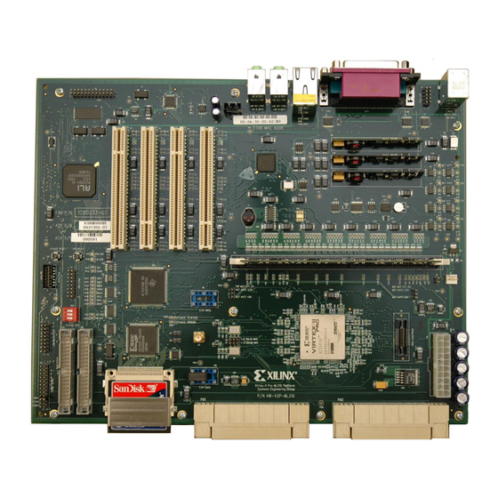
The ML310 CDROM contains documentation and tutorials, along with reference designs and data sheets. The most recent ML310 material can be found on the Xilinx web site at http://www.xilinx.com/ml310. The setup and quickstart documentation highlights the functionality of the ML310 using the applications shipped on the included CompactFlash card. - Page 18 Chapter 2: ML310 Embedded Development Platform Figure 2-1: ML310 Board www.xilinx.com ML310 User Guide 1-800-255-7778 UG068 (v1.01) August 25, 2004 Get other manuals https://www.bkmanuals.com...
-
Page 19: Features
Port 5V PCI SMBus Slots Audio Figure 2-2: ML310 High-Level Block Diagram Features In addition to the Virtex-II Pro™ FPGA with the embedded PPC405, the ML310 board features the following: • ATX Motherboard formfactor • 256 MB DDR DIMM •... -
Page 20: Board Hardware
Bus. The following sections describe the main features of each of the peripherals and how they interface with the Xilinx Virtex-II Pro. The EDK Processor IP Reference Guide should be reviewed as well as each of the data sheets corresponding to the devices listed. All device data sheets are located on the ML310 CDROM. -
Page 21: Ddr Memory
Board Hardware II Pro FPGA I/O can be configured to use different IO standards such as SSTL2 as required on the DDR DIMM interface. Please review the ML310 Virtex-II Pro data sheet for more information regarding I/O standards. Figure 2-3 shows the top-level clocking for the ML310 board. -
Page 22: Ddr Signaling
The FPGA is capable of replicating up to three differential clock output pairs to the DIMM in order to support either registered or unbuffered DIMMs. The ML310 DDR interface is very flexible in the event different DDR memory is desired such as an unbuffered DIMM or increased memory size. - Page 23 AA24 DDR_DQM05 ddr_dm[3] AB30 DDR_DQM04 ddr_dm[4] DDR_DQM03 ddr_dm[5] DDR_DQM02 ddr_dm[6] DDR_DQM01 ddr_dm[7] DDR_DQM00 ddr_dqs[0] AG30 DDR_DQS07 ddr_dqs[1] AF30 DDR_DQS06 ddr_dqs[2] AA28 DDR_DQS05 ddr_dqs[3] DDR_DQS04 ddr_dqs[4] DDR_DQS03 ML310 User Guide www.xilinx.com UG068 (v1.01) August 25, 2004 1-800-255-7778 Get other manuals https://www.bkmanuals.com...
- Page 24 Chapter 2: ML310 Embedded Development Platform Table 2-1: Connections from FPGA to DIMM Interface, P7 XC2VP30 Pin DIMM UCF Signal Name Schem Signal Name (U37) (P7) ddr_dqs[5] DDR_DQS02 ddr_dqs[6] DDR_DQS01 ddr_dqs[7] DDR_DQS00 ddr_dq[0] AG28 DDR_DQ63 ddr_dq[1] AG26 DDR_DQ62 ddr_dq[2] AE26...
- Page 25 DDR_DQ00 The connections from the FPGA to the DDR DIMM support either a registered or an unbuffered DIMM. The only difference from a connectivity perspective is that the ML310 User Guide www.xilinx.com UG068 (v1.01) August 25, 2004 1-800-255-7778 Get other manuals https://www.bkmanuals.com...
-
Page 26: Serial Port Fpga Uart
"null-modem" type of cable which cross-wires the TX and RX signals from one end of the cable to the RX and TX signals on the other end is used. Since the ML310 is a DTE, use a “null modem” cable when connecting to another DTE such as a PC. -
Page 27: System Ace Cf Controller
The RS-232 port directly connected to the XC2VP30 is accessible by a 10 pin header(J4). An RS-232 mini-cable adapter included with the ML310 converts J4, 10 pin header, to a DB9 male connector. The adapter is a standard DTK/Intel IDC-10 to DB9 Male. The FPGA RS-... -
Page 28: Non-Volatile Storage
Chapter 2: ML310 Embedded Development Platform Non-Volatile Storage In addition to programming the FPGA and storing bitstreams, System ACE can be used for general use non-volatile storage. System ACE provides an MPU interface for allowing a microprocessor to access the CompactFlash, allowing the use of the CompactFlash as a file system. -
Page 29: Jtag
Board Hardware JTAG JTAG is a simple interface that provides for many uses. On the ML310 Hardware Platform, the primary uses include configuration of the XC2VP30, debugging software (similar to the CPU debug interface), and debugging hardware using the ChipScope™ Integrated Logic Analyzer (ILA). -
Page 30: Parallel Cable Iv Interface
16 pin connector (J13) used to interface the ML310 with a 2 Line by 16 character LCD Display, AND491GST. Access to the GPIO lines is handled by a simple register interface that is connected XC2VP30 GPIO signals. - Page 31 FPGA_LCD_DB0 LCD_DB0 FPGA_LCD_DB1 LCD_DB1 FPGA_LCD_DB2 LCD_DB2 FPGA_LCD_DB3 LCD_DB3 FPGA_LCD_DB4 LCD_DB4 FPGA_LCD_DB5 LCD_DB5 FPGA_LCD_DB6 LCD_DB6 FPGA_LCD_DB7 LCD_DB7 GND1 GND2 GND3 SN74LVCC3245A Figure 2-8: LEDs and LCD Connectivity ML310 User Guide www.xilinx.com UG068 (v1.01) August 25, 2004 1-800-255-7778 Get other manuals https://www.bkmanuals.com...
-
Page 32: Gpio Led Interface
Chapter 2: ML310 Embedded Development Platform GPIO LED Interface All LEDs connected to the GPIO lines illuminate Green when driven with a logic zero and extinguish with a logic one. Table 2-6 shows the connections for the GPIO LEDs from the FPGA to the non-inverting buffer (U36). -
Page 33: Cpu Debug And Cpu Trace
FPGA_LCD_RW CPU Debug and CPU Trace The ML310 board includes two CPU debugging interfaces, the CPU Debug (J12 header) and the Combined CPU Trace and Debug (P8 mictor) connector. These connectors can be used in conjunction with third party tools, or in some cases the Xilinx Parallel Cable IV, to debug software as it runs on the processor.The PowerPC... - Page 34 Chapter 2: ML310 Embedded Development Platform The PPC405 JTAG (Joint Test Action Group) Debug port complies with IEEE standard 1149.1-1990, IEEE Standard Test Access Port and Boundary Scan Architecture. This standard describes a method for accessing internal chip resources using a four-signal or five-signal interface.
-
Page 35: Cpu Debug Connector Pinout
IO requirements specified in the PCI Local Bus Specification, Revision 2.2. The majority of the ML310 features are accessed over the 33MHz/32 bit PCI Bus. The Virtex-II Pro Power PC405 Processors can gain access to the Primary PCI Bus through the EDK PCI Host Bridge IP. - Page 36 PCI bus and PCI devices. For more information on the PCI slot pinouts, refer to the PCI 2.2 Specification or review the ML310 schematics. The 5.0V PCI slots differ from the 3.3V slots. See the Important Instructions sheet (PN 0402263) packaged with the ML310 kit before using Universal PCI add-in cards with the ML310 board.
- Page 37 Table 2-10: PCI Controller Connections UCF Signal Name XC2VP30 Pin (U37) Description PCI_CLK0 PCI_P_CLK0 PCI_CLK1 PCI_P_CLK1 PCI_CLK2 PCI_P_CLK2 PCI_CLK3 PCI_P_CLK3 PCI_CLK4 PCI_P_CLK4 PCI_CLK5 PCI_P_CLK5 PCI_CLK5_FB PCI_P_CLK5 ML310 User Guide www.xilinx.com UG068 (v1.01) August 25, 2004 1-800-255-7778 Get other manuals https://www.bkmanuals.com...
- Page 38 Chapter 2: ML310 Embedded Development Platform Table 2-10: PCI Controller Connections (Continued) UCF Signal Name XC2VP30 Pin (U37) Description PCI_INTA PCI_INTB PCI_INTC PCI Interrupt Signals PCI_INTD PCI_INTE PCI_INTF PCI_REQ0_N PCI_REQ1_N PCI_REQ2_N PCI Request Signals PCI_REQ3_N PCI_REQ4_N PCI_GNT0_N PCI_GNT1_N PCI_GNT2_N PCI Grant Signals...
- Page 39 PCI_AD[26] PCI_AD[27] PCI_AD[28] PCI_AD[29] PCI_AD[30] PCI_AD[31] PCI_PAR PCI_P_PAR PCI_RST_N PCI_P_RST_N * Note: These signals are connected, but are not required for 32 bit only PCI systems. ML310 User Guide www.xilinx.com UG068 (v1.01) August 25, 2004 1-800-255-7778 Get other manuals https://www.bkmanuals.com...
-
Page 40: Ali South Bridge Interface, M1535D+, U15
Int. ALi South Bridge Interface, M1535D+, U15 The ALi M1535D+ South Bridge augments the ML310 with many of the basic features found on legacy Personal Computers (PCs). These basic PC features are only accessible over the PCI Bus as this is the only way to access the ALI M1535D+. A brief description of the ALi M1535D+ features employed on the ML310 board is discussed below. -
Page 41: Parallel Port Interface, Connector Assembly P1
Parallel Port modes such as Standard Mode (SPP), Enhanced Parallel Port (EPP) and IEEE 1284 Compatible ECP. The P1, female DB25, connector pinout is configured as per IEEE Std. 1284-1994. Please review the ALi M1535D+ data sheets for more detailed information. ML310 User Guide www.xilinx.com UG068 (v1.01) August 25, 2004 1-800-255-7778... -
Page 42: Serial Port Interface, Connector Assembly P1
DTE interfaces and meet the EIA/TIA-574 standard. The DB9 male connectors are labeled Serial Port A and B in the ML310 schematics. The DB9 connectors are part of the P1 connector assembly. Please note that Serial Port B is located adjacent to the PS/2 connector where COM1 in a legacy PC is traditionally located. -
Page 43: Usb, Connector Assembly J3
Table 2-15: ALi South Bridge USB Type-A connector, J3 A/B J3 (A/B) Signal Name Description Pin No. USB_VCC USB Power, 5.0V, MOSFET Isolated USB_DN USB Data - USB_DP USB Data + Ground ML310 User Guide www.xilinx.com UG068 (v1.01) August 25, 2004 1-800-255-7778 Get other manuals https://www.bkmanuals.com... -
Page 44: Ide, Connectors J15 And J16
Chapter 2: ML310 Embedded Development Platform IDE, connectors J15 and J16 Supports a 2-channel UltraDMA-133 IDE Master controller independently connected to a Primary 40 Pin IDC connector (J16) and a Secondary 40 Pin IDC connector (J15). Please review the ALi M1535D+ Data sheets for more detailed information. -
Page 45: Gpio, Connector J5
Table 2-18 shows the connections from the ALi, M1535D+, GPIO signals available at the GPIO header (J5). Please review the ALi M1535D+ Data sheets, located on the ML310 CDROM, for more detailed information. Table 2-18: GPIO Connections on Header J5... -
Page 46: Ac97 Audio
LM4880 (U2). The audio jacks are available on the J1 and J2 connector assemblies. Please consult the M1535D+, LM4550 and LM4880 data sheets in conjunction with the ML310 schematics for more details on the ML310 Audio interface. Table 2-19 describes the audio jacks available to the user on the ML310. -
Page 47: Ps/2 Keyboard/Mouse Interface, Connector P2
Fuse protected power to Keyboard and Mouse Flash ROM, U4 The ALi South Bridge supports 4 Mbit Flash memory interface. The ML310 provides connectivity to an AM29F040B 4-Megabit (512 K x 8-Bit) Flash (U4) via the ALi M1535D+ ROM interface. Please review the ALi M1535D+ Data sheets for more detailed information. -
Page 48: Intel Gd82559, U11, 10/100 Ethernet Controller
The EEPROM provides power-on initialization for hardware and software configuration parameters. The ML310 board utilizes the 82559 10/100 Ethernet capability via FPGA PCI host bridge accesses over the PCI Bus. The 82559 is only accessible over the PCI bus, this includes programming of its power-on initialization EEPROM. -
Page 49: Iic/Smbus Interface
Board Hardware review the GD82559 Data sheet, located on the ML310 CDROM, for more detailed information. INTEL PCI_P_CLK2 GD82559 25MHz Ethernet MAC/PHY FPGA Vendor ID 0x8086 XC2VP30 RJ45 Device ID 0x1229 PCI_P_AD23 IDSEL PCI_BUS PCI_BUS EEPROM Figure 2-13: Intel GD82559 Ethernet Controller... - Page 50 Chapter 2: ML310 Embedded Development Platform Table 2-22 shows the FPGA connections to all SMBus and IIC devices. Table 2-22: SMBus and IIC Controller Connections UCF Signal Name XC2VP30 Pin Schem Signal Name iic_scl fpga_scl iic_sda fpga_sda iic_irq_n iic_irq_n iic_temp_crit_n* iic_therm_n * Note: This signal connects to U20 therm_l on the LM87.
- Page 51 ADDR: 0x5C VCC1V5 LM87 RTClock ADDR: 0xA2 RTC8566 EEPROM ADDR: 0xA0 24LC64 Note: Located on EEPROM DDR DIMM P7 Figure 2-14: SMBus and IIC Block Diagram ML310 User Guide www.xilinx.com UG068 (v1.01) August 25, 2004 1-800-255-7778 Get other manuals https://www.bkmanuals.com...
-
Page 52: Serial Peripheral Interface (Spi)
Chapter 2: ML310 Embedded Development Platform Table 2-23 lists the IIC devices and their associated addresses. Table 2-23: IIC Devices and Addresses Reference Device Address Description Designator LTC1694 SMBus accelerator that ensures data integrity with multiple devices on the SMBus. Enhances... -
Page 53: Spi Addressing
When the System ACE CF device is reset, it causes a re-configuration of the XC2VP30 FPGA. The ace file used to program the device is selected via dipswitch, SW3, settings. Please review the System ACE CF data sheet for more details, as it is located on the ML310 CDROM and also available on http://www.xilinx.com The front panel interface header (J23) can also drive the PB_SYSTEM_ACE_RESET signal. -
Page 54: System Ace Configuration Dipswitch, Sw3
SW2 push button for longer than 2 seconds. This action performs a CPU reset followed by a System ACE CF reset. Please review the ML310 schematics and the LTC1236 data sheet found on the ML310 CDROM for more details. -
Page 55: Front Panel Interface Connector, J23
(0.1inch pitch). J23 provides an optional means to control and gather status information from the ML310 board if it were to be enclosed similar to that of a desktop PC. The functionality listed below can easily be connected via a user build cable that connects to some collection of user created logic the could be used to control/monitor the functionality available via the Front Panel Interface. - Page 56 Chapter 2: ML310 Embedded Development Platform The front panel interface provides the following status information available at the J23 header. ♦ FPGA Configuration DONE Output intended for driving an LED ♦ IDE Disk access Output intended for driving an LED ♦...
-
Page 57: Jumpers
J10 (top) and J11 (bottom). The onboard regulated VTRX termination voltage can be configured for AC or DC coupling, 1.8V or 2.5V respectively. Table 2-26 shows the MGT VTRX voltage selections available on the ML310 board. Table 2-26: Jumper Selection for Top and Bottom MGT VTRX Voltages,J10/J11 Jumper... -
Page 58: Atx Power Distribution And Voltage Regulation
ATX Power Distribution and Voltage Regulation The ML310 board is shipped with a commercially available 250W ATX Power supply. All voltages required by the ML310 logic devices are derived from the 5.0V supply, except the +/- 12V supplies, as shown in Figure 2-17. - Page 59 An Antec, model SL250S, ATX Power Supply is delivered with your ML310. The Antec User’s Manual is provided in the Data sheets section on the ML310 CDROM. Prior to installation please read the Installation section of the Antec User’s Manual which describes the red voltage switch power setting on your Antec SL250S supply.
- Page 60 In addition to the MC34161D voltage monitors, the ML310 employs a SMBus device, LM87, which samples several of the same supply voltages when accessed over the System Management Bus or SMBus. More information on the SMBus features of the ML310 can be found in section “IIC/SMBus...
-
Page 61: High-Speed I/O
ML310 board through the PM1 and PM2 connectors. The plug, located on the ML310 board, is referred to as the host board connector; the receptacle, located on the personality module, is referred to as the adapter board connector. -
Page 62: Ml310 Pm Connectors
40 pair connector. Each connector has 40 differential pairs and several power and ground pins. Together, the two PM connectors on the ML310 support 158 high-speed I/O pins that can be user defined. The PM1 and PM2 signals are as follows: •... -
Page 63: Pm1 Connector
High-Speed I/O Figure 2-20 shows an edge view of the PM host board connectors on the ML310 board. PM1 Host Board Connector PM2 Host Board Connector Figure 2-20: Edge View of Host Board Connectors on ML310 Each signal pair on the PM1 and PM2 host board connectors has a wide ground pin on the... -
Page 64: Adapter Board Pm Connectors
Adapter Board PM Connectors Tyco Z-Dok+ adapter board connectors, part number 1367555-1 are the receptacle connectors on the personality modules that mate to the ML310 Tyco Z-Dok+ host board connectors, part number 1367550-5. The Tyco data sheet for part number 1367555-1 is available at http://www.z-dok.com/documents/1367555.pdf. -
Page 65: Pm1 Power And Ground
High-Speed I/O PM1 Power and Ground Table 2-29 shows the power and ground pins for the PM1 connector on the ML310. Table 2-29: PM1 Power and Ground Pins Pin Number Description Length Contact Order 1, 6 Ground Level 4 First 2, 5 2.5V... - Page 66 Chapter 2: ML310 Embedded Development Platform Table 2-31: PM1 Pinout (Continued) FPGA Bank PM1 Pin FPGA Pin Pin Description ML310 Schematic Net IO_L69P_0 PM_IO_82 2.5V IO_L69N_0 PM_IO_83 2.5V RXPPAD4 RXPPAD4_A25 RXNPAD4 RXNPAD4_A24 RXPPAD7 RXPPAD7_A12 RXNPAD7 RXNPAD7_A11 TXPPAD16 TXPPAD16_AK6 TXNPAD16 TXNPAD16_AK7...
- Page 67 High-Speed I/O Table 2-31: PM1 Pinout (Continued) FPGA Bank PM1 Pin FPGA Pin Pin Description ML310 Schematic Net IO_L02N_7 PM_IO_85 2.5V IO_L44N_1 PM_IO_3V_21 IO_L44P_1 PM_IO_3V_20 IO_L08P_1 PM_IO_3V_8 IO_L07P_1 PM_IO_3V_6 IO_L03P_1 PM_IO_3V_2 IO_L38P_1 PM_IO_3V_14 IO_L67P_0 PM_IO_78 2.5V IO_L67N_0 PM_IO_79 2.5V TXNPAD4...
-
Page 68: Ml310 Pm2 User I/O
ML310 PM2 User I/O The PM2 connector makes most of the LVDS pairs available to the user, along with single- ended signals. Table 2-32 shows the pinout for the PM2 connector on the ML310. Table 2-32: PM2 Pinout FPGA Bank PM2 Pin... - Page 69 High-Speed I/O Table 2-32: PM2 Pinout (Continued) FPGA Bank PM2 Pin FPGA Pin Pin Description ML310 Schematic Net IO_L57N_3 PM_IO_53 2.5V IO_L57P_3 PM_IO_52 2.5V IO_L85N_3 PM_IO_61 2.5V IO_L85P_3 PM_IO_60 2.5V IO_L50N_3 PM_IO_39 2.5V IO_L50P_3 PM_IO_38 2.5V IO_L55N_3 PM_IO_49 2.5V IO_L55P_3 PM_IO_48 2.5V...
- Page 70 Chapter 2: ML310 Embedded Development Platform Table 2-32: PM2 Pinout (Continued) FPGA Bank PM2 Pin FPGA Pin Pin Description ML310 Schematic Net IO_L44N_3 PM_IO_27 2.5V IO_L43P_3 PM_IO_24 2.5V IO_L43N_3 PM_IO_25 2.5V IO_L33P_3 PM_IO_10 2.5V IO_L33N_3 PM_IO_11 2.5V IO_L34P_3 PM_IO_12 2.5V...
Need help?
Do you have a question about the ML310 and is the answer not in the manual?
Questions and answers