Xilinx ML505 User Manual
Evaluation platform
Hide thumbs
Also See for ML505:
- Quick start manual (29 pages) ,
- Quick start manual (41 pages) ,
- Getting started tutorial (31 pages)
Table of Contents
Advertisement
Quick Links
Advertisement
Table of Contents

Related Manuals for Xilinx ML505


Summary of Contents for Xilinx ML505
- Page 1 ML505/ML506/M ML505/ML506/ML507 L507 Evaluation Evaluation Platform Platform User Guide [optional] User Guide UG347 (v3.1.1) October 7, 2009 [optional] UG347 (v3.1.1) October 7, 2009 Downloaded from Elcodis.com electronic components distributor...
- Page 2 Xilinx. Xilinx expressly disclaims any liability arising out of your use of the Documentation. Xilinx reserves the right, at its sole discretion, to change the Documentation without notice at any time. Xilinx assumes no obligation to correct any errors contained in the Documentation, or to advise you of any corrections or updates.
- Page 3 “17. System ACE and CompactFlash Connector,” page 28 11/10/08 “Configuration Options,” page 53. Updated Platform Flash memory to Platform Flash PROM throughout. 10/07/09 3.1.1 Minor typographical edit. UG347 (v3.1.1) October 7, 2009 www.xilinx.com ML505/ML506/ML507 Evaluation Platform Downloaded from Elcodis.com electronic components distributor...
- Page 4 ML505/ML506/ML507 Evaluation Platform www.xilinx.com UG347 (v3.1.1) October 7, 2009 Downloaded from Elcodis.com electronic components distributor...
-
Page 5: Table Of Contents
20. Xilinx XC95144XL CPLD ........ - Page 6 ............53 JTAG (Xilinx Download Cable and System ACE Controller) Configuration ..53 Platform Flash PROM Configuration .
-
Page 7: Preface: About This Guide
The ML50x evaluation platforms enable designers to investigate and experiment with features of Virtex®-5 FPGAs. This user guide describes the features and operation of the ML505 (LXT), ML506 (SXT), and ML507 (FXT) Evaluation Platforms. Guide Contents This manual contains the following chapters: •... -
Page 8: Additional Support Resources
Additional Support Resources To search the database of silicon and software questions and answers, or to create a technical support case in WebCase, see the Xilinx website at: http://www.xilinx.com/support. Typographical Conventions This document uses the following typographical conventions. An example illustrates each convention. -
Page 9: Online Document
Virtex-5 Data Red text location in another document Sheet Go to http://www.xilinx.com Blue, underlined text Hyperlink to a website (URL) for the latest documentation. ML505/ML506/ML507 Evaluation Platform www.xilinx.com UG347 (v3.1.1) October 7, 2009 Downloaded from Elcodis.com electronic components distributor... - Page 10 Preface: About This Guide www.xilinx.com ML505/ML506/ML507 Evaluation Platform UG347 (v3.1.1) October 7, 2009 Downloaded from Elcodis.com electronic components distributor...
-
Page 11: Overview
Platform Overview ML505, ML506, and ML507 Evaluation Platforms (referred to as ML50x in this guide) enable designers to investigate and experiment with features of the Virtex-5 LXT, SXT, and FXT FPGAs. This user guide describes the features and operation of these platforms. - Page 12 Chapter 1: ML505/ML506/ML507 Evaluation Platform • RS-232 serial port, DB9 and header for second serial port • 16-character x 2-line LCD display • One 8-Kb IIC EEPROM and other IIC capable devices • PS/2 mouse and keyboard connectors • Video input/output ♦...
-
Page 13: Package Contents
For information about the Virtex-5 family of FPGA devices, including product highlights, data sheets, user guides, and application notes, see the Virtex-5 FPGA website at www.xilinx.com/virtex5. Additional information is available from the data sheets and application notes from the component manufacturers. -
Page 14: Block Diagram
GTP: PCIe 1x UG347_03_110807 Figure 1-1: Virtex-5 FPGA ML50x Evaluation Platform Block Diagram Related Xilinx Documents Prior to using the ML50x Evaluation Platform, users should be familiar with Xilinx resources. See Appendix C, “References” for direct links to Xilinx documentation. See the following locations for additional documentation on Xilinx tools and solutions: •... -
Page 15: Detailed Description
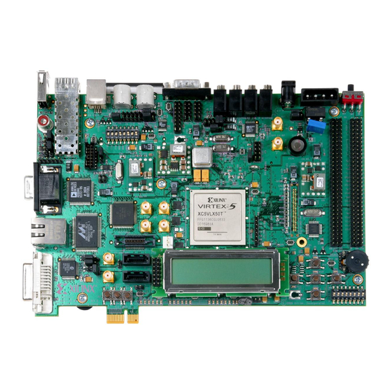
(back). The numbered sections on the pages following the figures contain details on each feature. Diff Output Pair Keybd Mouse System ACE Reset Diff Input Pair UG347_01_102907 Figure 1-2: Detailed Description of Virtex-5 FPGA ML505 Components (Front) ML505/ML506/ML507 Evaluation Platform www.xilinx.com UG347 (v3.1.1) October 7, 2009 Downloaded from Elcodis.com electronic components distributor... - Page 16 Chapter 1: ML505/ML506/ML507 Evaluation Platform UG347_02_112906 Figure 1-3: Detailed Description of Virtex-5 FPGA ML505 Components (Back) Note: The label on the CompactFlash (CF) card shipped with your board might differ from the one shown. www.xilinx.com ML505/ML506/ML507 Evaluation Platform UG347 (v3.1.1) October 7, 2009 Downloaded from Elcodis.com...
-
Page 17: Virtex-5 Fpga
Detailed Description 1. Virtex-5 FPGA A Xilinx Virtex-5 FPGA is installed on the board. See Appendix A, “Board Revisions” device details. Configuration The board supports configuration in all modes: JTAG, Master Serial, Slave Serial, Master SelectMAP, Slave SelectMAP, Byte-wide Peripheral Interface (BPI) Up, BPI Down, and SPI modes. -
Page 18: Digitally Controlled Impedance
The board is only tested for DDR2 SDRAM operation at a 400 MHz data rate. Faster data rates might be possible but are not tested. MIG Compliance The ML50x DDR2 interface is MIG pinout compliant. The MIG DDR2 routing guidelines outlined in the Xilinx Memory Interface Generator (MIG) User Guide [Ref 17] have been achieved. -
Page 19: Ddr2 Memory Expansion
100-MHz oscillator and is powered by the 3.3V supply. The board also provides an IDT5V9885 (U8) EEPROM programmable clock generator device. This device is used to generate a variety of clocks to the board peripherals and ML505/ML506/ML507 Evaluation Platform www.xilinx.com UG347 (v3.1.1) October 7, 2009 Downloaded from Elcodis.com... -
Page 20: Lcd Brightness And Contrast Adjustment
33 MHz to the Xilinx System ACE CF (U2) • 33 MHz, 27 MHz, and a differential 200 MHz clock to the Xilinx FPGA If users change the factory default configuration of the clock generator chip, the related reference design material might not work as designed. Instructions for returning the... -
Page 21: User And Error Leds (Active-High)
GPIO LED 4 Green DS12 GPIO LED 5 Green AD25 DS11 GPIO LED 6 Green AD24 DS10 GPIO LED 7 Green AE24 Error 1 Error 2 ML505/ML506/ML507 Evaluation Platform www.xilinx.com UG347 (v3.1.1) October 7, 2009 Downloaded from Elcodis.com electronic components distributor... -
Page 22: User Pushbuttons (Active-High)
Chapter 1: ML505/ML506/ML507 Evaluation Platform 8. User Pushbuttons (Active-High) Five active-High user pushbuttons are available for general purpose usage and are arranged in a North-East-South-West-Center orientation (only the center one is cited in Figure 1-2, page 15). Table 1-7 summarizes the user pushbutton connections. -
Page 23: Single-Ended Expansion I/O Connectors
I/O connector. Table 1-10: Expansion I/O Single-Ended Connections (J6) J6 Pin Schematic Net Name FPGA Pin HDR1_2 HDR1_4 HDR1_6 HDR1_8 HDR1_10 HDR1_12 HDR1_14 HDR1_16 ML505/ML506/ML507 Evaluation Platform www.xilinx.com UG347 (v3.1.1) October 7, 2009 Downloaded from Elcodis.com electronic components distributor... -
Page 24: Other Expansion I/O Connectors
Chapter 1: ML505/ML506/ML507 Evaluation Platform Table 1-10: Expansion I/O Single-Ended Connections (J6) (Cont’d) J6 Pin Schematic Net Name FPGA Pin HDR1_18 HDR1_20 HDR1_22 HDR1_24 HDR1_26 AA34 HDR1_28 AD32 HDR1_30 HDR1_32 HDR1_34 HDR1_36 AH34 HDR1_38 AE32 HDR1_40 AG32 HDR1_42 AH32 HDR1_44... - Page 25 GPIO Switch West GPIO_LED_S AG12 LED South SW11 (S) GPIO Switch South GPIO_LED_E AG23 LED East SW12 (E) GPIO Switch East GPIOLED 0 GPIO LED 0 ML505/ML506/ML507 Evaluation Platform www.xilinx.com UG347 (v3.1.1) October 7, 2009 Downloaded from Elcodis.com electronic components distributor...
-
Page 26: Stereo Ac97 Audio Codec
Chapter 1: ML505/ML506/ML507 Evaluation Platform Table 1-11: Additional Expansion I/O Connections (J5) (Cont’d) J5 Pin Label FPGA Pin Description GPIOLED 1 GPIO LED 1 GPIOLED 2 GPIO LED 2 GPIOLED 4 GPIO LED 4 Not Connected Not Connected IIC_SCL_EXP Expansion IIC SCL... -
Page 27: Rs-232 Serial Port
A DVI monitor can be connected to the board directly. A VGA monitor can also be connected to the board using the supplied DVI-to-VGA adaptor. The Chrontel CH7301C is controlled by way of the video IIC bus. ML505/ML506/ML507 Evaluation Platform www.xilinx.com UG347 (v3.1.1) October 7, 2009 Downloaded from Elcodis.com... -
Page 28: Ps/2 Mouse And Keyboard Ports
AC adapter. 17. System ACE and CompactFlash Connector The Xilinx System ACE CompactFlash (CF) configuration controller allows a Type I CompactFlash card to program the FPGA through the JTAG port. Both hardware and software data can be downloaded through the JTAG port. The System ACE controller supports up to eight configuration images on a single CompactFlash card. - Page 29 CompactFlash, with the xilinx.sys file located in the root directory. The xilinx.sys file is used by the System ACE CF controller to define the project directory structure, which consists of one main folder containing eight sub-folders used to store the eight ACE files containing the configuration images.
-
Page 30: Zbt Synchronous Sram
20. Xilinx XC95144XL CPLD A Xilinx XC95144XL CPLD provides general-purpose glue logic for the board. The CPLD is located under the removable LCD and is not visible in Figure 1-2, page 15. -
Page 31: 100/1000 Tri-Speed Ethernet Phy
2.5V or DIS_FC = 1 DIS_SLEEP = 1 HWCFG_MODE[3] = 1 LED_LINK10 (Set by J22) CONFIG6 LED_RX SEL_BDT = 0 INT_POL = 1 75/50Ω = 0 ML505/ML506/ML507 Evaluation Platform www.xilinx.com UG347 (v3.1.1) October 7, 2009 Downloaded from Elcodis.com electronic components distributor... -
Page 32: Usb Controller With Host And Peripheral Ports
EEPROM. 23. Xilinx XCF32P Platform Flash PROM Configuration Storage Devices The two onboard Xilinx XCF32P Platform Flash PROM configuration storage devices offer a convenient and easy-to-use configuration solution for the FPGA. The Platform Flash PROM holds up to two separate configuration images (up to four with compression) that can be accessed through the configuration address switches. -
Page 33: Jtag Configuration Port
The JTAG configuration port for the board (J1) allows for device programming and FPGA debug. The JTAG port supports the Xilinx Parallel Cable III, Parallel Cable IV, or Platform USB cable products. Third-party configuration products might also be available. The JTAG chain can also be extended to an expansion board by setting jumper J21 accordingly. -
Page 34: Ac Adapter And Input Power Switch/Jack
Chapter 1: ML505/ML506/ML507 Evaluation Platform To USB and PS/2 5V Brick 1.0V PT Host 220W 16A Switching Regulator To FPGA Core 2.5V TPS74401 3.3V PT Host 240W 3A LDO To FPGA I/O 10A Switching Regulator 2.5V TPS74401 3A LDO To FPGA V CCAUX 1.2V... -
Page 35: Done Led
System ACE controller configures the FPGA from the CF card whenever a card is inserted or the SYSACE RESET button is pressed. Notes: 1. Reserved for future use. Not currently implemented. ML505/ML506/ML507 Evaluation Platform www.xilinx.com UG347 (v3.1.1) October 7, 2009 Downloaded from Elcodis.com... -
Page 36: Encryption Key Battery
The ML50x board has a 32-Mb SPI Flash (ST Microelectronics M25P32). The SPI Flash can be used for FPGA configuration or to hold user data. The SPI Flash can be in-system programmed using a Xilinx download cable with flying leads attached to header J2 (Figure 1-6). -
Page 37: Iic Fan Controller And Temperature/Voltage Monitor
Table 1-20 shows the connections for the VGA input video codec. Table 1-20: VGA Interface Connections Net Name FPGA Pin VGA_IN_RED0 VGA_IN_RED1 VGA_IN_RED2 VGA_IN_RED3 VGA_IN_RED4 ML505/ML506/ML507 Evaluation Platform www.xilinx.com UG347 (v3.1.1) October 7, 2009 Downloaded from Elcodis.com electronic components distributor... -
Page 38: Jtag Trace/Debug
Chapter 1: ML505/ML506/ML507 Evaluation Platform Table 1-20: VGA Interface Connections (Cont’d) Net Name FPGA Pin VGA_IN_RED5 VGA_IN_RED6 VGA_IN_RED7 VGA_IN_GREEN0 VGA_IN_GREEN1 VGA_IN_GREEN2 VGA_IN_GREEN3 VGA_IN_GREEN4 VGA_IN_GREEN5 VGA_IN_GREEN6 VGA_IN_GREEN7 VGA_IN_BLUE0 VGA_IN_BLUE1 VGA_IN_BLUE2 VGA_IN_BLUE3 VGA_IN_BLUE4 VGA_IN_BLUE5 VGA_IN_BLUE6 VGA_IN_BLUE7 VGA_IN_CLAMP VGA_IN_COAST VGA_IN_EVEN_B VGA_IN_VSOUT VGA_IN_HSOUT VGA_IN_SOGOUT 37. - Page 39 38-pin Mictor connector that combines the CPU Trace and the CPU Debug interfaces for high-speed, controlled-impedance signaling. Note: MICTOR_* pins are only available on the ML507 board. These pins are not connected on the ML505 and ML506 boards. Mictor 38 (P22) MICTOR_37 TRC_TS6...
- Page 40 Chapter 1: ML505/ML506/ML507 Evaluation Platform Table 1-21: CPU Trace/Debug Connection to FPGA (Cont’d) Pin Name FPGA Pin (U1) Mictor Pin (P22) BDM Pin (J51) CPU_TDO TRC_VSENSE CPU_TCK MICTOR_16 CPU_TMS MICTOR_18 FPGA_CS0_B AF21 (CPU_TDI) MICTOR_20 CPU_TRST MICTOR_22 MICTOR_23 TRC_TS1O AF10 MICTOR_25...
-
Page 41: Cpu Jtag Header Pinout
FPGA pins. Table 1-22: CPU JTAG Connection to FPGA Pin Name FPGA Pin (U1) Connector Pin (J12) CPU_TDO FPGA_SC0_B (CPU_TDI) AF21 CPU_TRST_N CPU_TCK CPU_TMS PC4_HALT_B (CPU_HALT_N) ML505/ML506/ML507 Evaluation Platform www.xilinx.com UG347 (v3.1.1) October 7, 2009 Downloaded from Elcodis.com electronic components distributor... -
Page 42: Rotary Encoder
Chapter 1: ML505/ML506/ML507 Evaluation Platform 38. Rotary Encoder The board provides connectivity to a rotary encoder (Panasonic EVQWK4001) with 15 detents, pushbutton, and two phase output signals for direction of rotation interpretation. One complete revolution of the rotary wheel produces 15 pulses that are output on nets FPGA_ROTARY_INCA and FPGA_ROTARY_INCB. -
Page 43: Pci Express Interface
CPLD Integrated Endpoint block wake signal PCIE_WAKE_B available on CPLD Notes: 1. For ML505/ML506 platforms, access is through GTP0 of GTP_X0Y1. 2. For ML507 platforms, access is through GTX0 of GTX_X0Y2. ML505/ML506/ML507 Evaluation Platform www.xilinx.com UG347 (v3.1.1) October 7, 2009 Downloaded from Elcodis.com... -
Page 44: Serial-Ata Host Connectors
The SATA physical interface can carry GTP/GTX signals up to 1.5 Gb/s for general-purpose usage. The board ships with a special Xilinx SATA crossover cable that is used as a loopback connection between the two SATA host connectors for loopback testing and bit error rate testing (BERT). - Page 45 SFP Signal FPGA Pin (U1) Description CLKBUF_Q0_P AC-coupled, LVDS, GTP REFCLK pair. CLKBUF_Q0_N SFP_RX_P Receive pair. • ML505/ML506: GTP0 of GTP_X0Y4 SFP_RX_N • ML507: GTX0 of GTX_X0Y5 SFP_TX_P Transmit pair. • ML505/ML506: GTP0 of GTP_X0Y4 SFP_TX_N • ML507: GTX0 of...
-
Page 46: Gtp/Gtx Clocking Circuitry
Table 1-29 provides a summary of the GTP clock sources. Table 1-29 provides a summary of the GTX clock sources. Table 1-29: GTP Clock Sources (ML505/ML506) GTP Pairs GTP REFCLK Diff Pair GTP Tile Frequency Location... -
Page 47: Sata Gtp/Gtx Transceiver Clock Generation
125-MHz LVDS clock from an inexpensive 25-MHz crystal oscillator. This clock is sent to the GTPs driving the SGMII or onboard loopback interfaces. Series AC coupling capacitors are also present to allow the clock input of the FPGA to set the common mode voltage. ML505/ML506/ML507 Evaluation Platform www.xilinx.com UG347 (v3.1.1) October 7, 2009 Downloaded from Elcodis.com... -
Page 48: Soft Touch Landing Pad
Chapter 1: ML505/ML506/ML507 Evaluation Platform 44. Soft Touch Landing Pad An Agilent Pro Series soft touch landing pad is available for use with a logic analyzer. The landing pad is designed for use with the Agilent E5404/06A 34-channel single-ended probe. The soft touch landing pad shares some pins with the XGI header. Signals that the... -
Page 49: System Monitor
14]. Please note that the circuitry connected to the 16 AUX channels on the ML50x are connected in a non-optimal fashion as they are implemented without anti-alias filtering at the FPGA. This tradeoff was ML505/ML506/ML507 Evaluation Platform www.xilinx.com UG347 (v3.1.1) October 7, 2009 Downloaded from Elcodis.com... - Page 50 (VAUXP[15:0], VAUXN[15:0]). The System Monitor is fully functional on power up, and measurement data can be accessed via the JTAG port pre-configuration. The Xilinx ChipScope™ Pro tool [Ref 24] provides access to the System Monitor over the JTAG port. The System Monitor control logic implements some common monitoring features.
- Page 51 HDR2_20_DIFF_2_P VAUXN[12] J4-14 HDR2_14_DIFF_1_N VAUXP[12] J4-16 HDR2_16_DIFF_1_P VAUXN[13] J4-10 HDR2_10_DIFF_0_N VAUXP[13] J4-12 HDR2_12_DIFF_0_P VAUXN[14] J4-6 HDR2_6_SM_7_N VAUXP[14] J4-8 HDR2_8_SM_7_P VAUXN[15] J4-2 HDR2_2_SM_8_N VAUXP[15] J4-4 HDR2_4_SM_8_P ML505/ML506/ML507 Evaluation Platform www.xilinx.com UG347 (v3.1.1) October 7, 2009 Downloaded from Elcodis.com electronic components distributor...
-
Page 52: Iic Buses
Chapter 1: ML505/ML506/ML507 Evaluation Platform IIC Buses The board supports four IIC buses; Main, Video, SFP, and DDR2. Each of the IIC buses has 1K pull-ups on its SCL and SDA signals. Table 1-35 describes the IIC devices attached to each of the four buses. -
Page 53: Configuration Options
The following section provides an overview of the possible ways the FPGA can be configured. JTAG (Xilinx Download Cable and System ACE Controller) Configuration The FPGA, two Platform Flash PROMs, and CPLD can be configured through the JTAG port. The JTAG chain of the board is illustrated in Figure 1-9. -
Page 54: Platform Flash Prom Configuration
Chapter 1: ML505/ML506/ML507 Evaluation Platform Pressing the System ACE reset button also causes the System ACE controller to program the FPGA if a CompactFlash card is present. Platform Flash PROM Configuration The Platform Flash PROMs can also be used to program the FPGA. A Platform Flash PROM can hold up to two configuration images (up to four with compression), which are selectable by the two least significant bits of the configuration address DIP switches. -
Page 55: Appendix A: Board Revisions
A-1). Table A-1: ML50x Platform Details Platform Device Package Product Revision Description XC5VLX50T-1C 1FFG1136 Rev A 0483688-03 and up ML505 is an LXT platform ML505 that supports RocketIO GTP 0483688-01 XC5VLX50T-1CES 1FFG1136 Rev A transceivers 0483688-02 XC5VSX50T-1C 1FFG1136 Rev A... - Page 56 ML505/ML506/ML507 Evaluation Platform UG347 (v3.1.1) October 7, 2009 Downloaded from Elcodis.com electronic components distributor...
-
Page 57: Appendix B: Programming The Idt Clock Chip
• Xilinx download cable • JTAG flying wires Downloading to the ML50x Board Connect a Xilinx download cable to the board using flying leads connected to jumper (Figure B-1). CLK Prog 3.3V UG347_apdx_a_02_020807 Figure B-1: J3 IDT5V9885 JTAG Connector Click Start →... - Page 58 To finish programming the chip, cycle the power by turning off the board power switch. After turning the board back on, verify that the clock frequencies are correct. www.xilinx.com ML505/ML506/ML507 Evaluation Platform UG347 (v3.1.1) October 7, 2009 Downloaded from Elcodis.com...
- Page 59 Memory Solutions Web page offers the following material supporting the Memory Interface Generator (MIG) tool: 16. WP260, Memory Interfaces Made Easy with Xilinx FPGAs and the Memory Interface Generator. 17. UG086, Xilinx Memory Interface Generator (MIG) User Guide (for registered users). Demos on Demand, Memory Interface Solutions with Xilinx FPGAs.
- Page 60 ChipScope Pro Analyzer: 24. UG029, ChipScope Pro Software and Cores User Guide. 25. UG213, ChipScope Pro Serial I/O Toolkit User Guide. www.xilinx.com ML505/ML506/ML507 Evaluation Platform UG347 (v3.1.1) October 7, 2009 Downloaded from Elcodis.com electronic components distributor...
Need help?
Do you have a question about the ML505 and is the answer not in the manual?
Questions and answers