
Related Manuals for Kontron VX3030


Summary of Contents for Kontron VX3030
- Page 1 » VX3030 « 3U VPX Computing Node User's Guide CA.DT.A87-5e October 2012 If it's embedded, it's Kontron.
- Page 2 Preliminary Version 02-2011 Copyright © 2012 Kontron AG. All rights reserved. All data is for information purposes only and not guaranteed for legal purposes. Information has been carefully checked and is believed to be accurate; however, no responsibility is assumed for inaccuracies. Kontron and the Kontron logo and all other trademarks or registered trademarks are the property of their respective owners and are recognized.
- Page 3 This document contains information proprietary to Kontron. It may not be copied or transmitted by any means, disclosed to others, or stored in any retrieval system or media without the prior written consent of Kontron or one of its authorized agents.
- Page 4 Therefore, in the interest of your own safety and of the correct operation of your new Kontron product, you are requested to conform with the following guidelines.
- Page 5 General Instructions on Usage In order to maintain Kontron’s product warranty, this product must not be altered or modified in any way. Changes or modifications to the device, which are not explicitly approved by Kontron and described in this manual or received from Kontron’s Technical Support as a special handling instruction, will void your warranty.
-
Page 6: Table Of Contents
VX3030 User's Guide Table Of Contents Table Of Contents Chapter 1 - Introduction ............ - Page 7 VX3030 User's Guide Table Of Contents 3.1.2 Watchdog Timer ............. .
- Page 8 VX3030 User's Guide Table Of Contents 7.5.7 I2C System Management Connector ..........
- Page 9 ..........Figure 4: VX3030 Front Panel I/O Interfaces .
- Page 10 ............Figure 46: VX3030-RTM Reset Push Button .
- Page 11 ............. . . Table 4: VX3030 Main Characteristics .
-
Page 12: Table 5: Environmental Specifications
........Table 43: VX3030-RC Order Code . -
Page 13: Chapter 1 - Introduction
Platform Controller Hub (PCH) QM57 with numerous Gigabit Ethernet, SATA, USB 2.0 and PCIe channels. The VX3030 board comes with EFI BIOS and supports Linux. It is covered by Kontron's long term supply program, which guarantees customers multi-year supply of the product beyond its active life. -
Page 14: Manual Overview
1.1.2 Audience This guide is written to cover, as far as possible the range of people who will handle or use the VX3030, from unpackers/inspectors, through system managers and installation technicians to hardware and software engineers. Most chapters assume a certain amount of knowledge on the subjects of single board computer architecture, interfaces, peripherals, system, cabling, grounding and communications. -
Page 15: Terminology, Definitions And Abbreviations
VX3030 will be associated to the 3U VPX board > VX3030-SA will be associated to the standard air-cooled commercial version of the board. > VX3030-RA will be associated to the rugged air-cooled version of the board. > VX3030-RC will be associated to the rugged conduction-cooled version of the board. -
Page 16: Board Overview
The VX3030 computing node is a VPX computing blade for parallel data and signal processing application. The VX3030 is the ideal building block for intensive parallel computing workloads where a cluster of VX3030s is used in full mesh or switched OpenVPX environments. Target applications include radar, sonar, imaging systems, airborne fighters, and unmanned aerial vehicle (UAV) radar, as well as rugged multi-display consoles. - Page 17 Please contact Kontron for further information regarding other operating systems and software support. Harsh Environments The VX3030 has been designed to use the same PCB for both air and conduction-cooled boards. Build variants span a complete range of temperature, shock and vibration requirements as specified in the VITA 47 standards.
-
Page 18: Block Diagram
Introduction VX3030 User's Guide 1.3.2 Block Diagram Figure 2: VX3030 Block Diagram Page 6 CA.DT.A87-5e... -
Page 19: Figure 3: Vx3030 Functional Block Diagram
VX3030 User's Guide Introduction Figure 3: VX3030 Functional Block Diagram CA.DT.A87-5e Page 7... -
Page 20: Ordering Information
Introduction VX3030 User's Guide 1.3.3 Ordering Information Manufacturing Options > CPU Frequency: ........ -
Page 21: I/O Interfaces
Not available on RC (Rugged Conduction-Cooled) boards Serial Graphics Reset CPU LEDs L1 L2 L3 Figure 4: VX3030 Front Panel I/O Interfaces Function Description See also Serial Ports COM: 1x EIA-232/EIA-485 UART interface for CPU on RJ-12 Section 4.1.1 for Pin connector. -
Page 22: Figure 5: Vx3030 Rear I/O Distribution
> VITA 65 (OpenVPX System specification) 12 V, 5V, 3.3V, 3 GPIOs, 2 I2C x4 PCIe, 2 SATA, 2 USB, 3 GETH, 3 GPIOs 2 SATA, 2 USB, 2 Display Port, 2 Serial Lines, x1 PCIe Figure 5: VX3030 Rear I/O Distribution Page 10 CA.DT.A87-5e... -
Page 23: Table 3: Rear I/O Interfaces
VX3030 User's Guide Introduction Function Description See also > 1 x4 gen2 PCIe non transparent capability, on P1. Optional use of PCIe common reference clock feature. PCI Express > 1 x1 additional PCIe interface, gen1, on P2 > 2 SATA II link on P1 SATA Storage Section 4.3 for... -
Page 24: Components Layout
Components Layout DDR3-SDRAM USB Mezzanine Slot Battery Mezzanine Slot PCIe SW Intel Intel PEX8609 QM57 Jumper Core i7 “Clear CMOS” Figure 6: VX3030 Components Layout (Top view) MicroSwitch DDR3-SDRAM MicroSwitch MicroSwitch Figure 7: VX3030 Components Layout (Bottom view) Page 12 CA.DT.A87-5e... -
Page 25: Technical Specification
VX3030 User's Guide Introduction 1.3.6 Technical Specification Form Factor Form Factor 3U VPX, single slot, 0.8 inch or 1 inch pitch for Standard Air (SA), 0.8 inch pitch for Rugged conduction-cooled (RC). Processor: Intel® Core™ i7 Processor Intel® Core™ i7 -6xx at 2 GHz. -
Page 26: Environmental Specifications
CPU Debug XDP port for CPU extended debug port connection (only available on a debug Interface connector and need additional test board for XDP access) Table 4: VX3030 Main Characteristics Environmental Specifications ENVIRONMENTAL SPECIFICATIONS SA - Standard Commercial RC - Rugged Conduction-Cooled... -
Page 27: Technical Specifications
40°C 55°C MTBF (hours) 279 497 h 198 551 h 36 449 h 54 242 h 43 345 h 9 186 h Table 6: VX3030-SA22-00000 MTBF Data VX3030-RC22-0N000 GB (Hours) AIC (Hours) NS (Hours) ARW (Hours) 25°C 40°C 40°C 25°C 40°C... -
Page 28: Related Publications
VX3030 Hardware Release Notes CA.DT.A88 Firmware VX3030 Boards AMI-BIOS User Reference Manual SD.DT.F81 Software VX3030 Boards Release Note Fedora 12 on VX6060 and VX3030 SD.DT.F72 Systems VX3030 Boards EZ3-VX3030- Getting Started SD.DT.F75 EZ3-VX3030- Quick Start SD.DT.F76 Table 8: Related Publications Page 16 CA.DT.A87-5e... -
Page 29: Chapter 2 - Installation
Safety Requirements The following safety precautions must be observed when installing or operating the VX3030. Kontron assumes no responsibility for any damage resulting from failure to comply with these requirements. -
Page 30: Board Identification
Installation VX3030 User's Guide Board Identification The VX3030 boards are identified by labels fitted to the top side of the board. Top Side "PLD A reference" label. "Identification" label: Order Code, Serial Number, Variant, E.C. Level Ethernet MAC addresses Figure 8: VX3030 Identification (Top Side) Page 18 CA.DT.A87-5e... -
Page 31: Board Configuration
VX3030 User's Guide Installation Board Configuration Jumper Jumper Figure 9: VX3030 Board Configuration (Top view) Two jumpers are available on the VX3030 : > Clear CMOS > Secondary RTC Reset Description Clear CMOS Secondary RTC Reset Clear CMOS Secondary RTC... -
Page 32: Figure 10: Vx3030 Board Configuration (Bottom View)
VX3030 User's Guide Microswitches MicroSwitch SW3 MicroSwitch SW2 1 2 3 4 MicroSwitch SW1 1 2 3 4 Figure 10: VX3030 Board Configuration (Bottom view) Three 4-bit microswitches are available on the VX3030: SW1, SW2 and SW3 Page 20 CA.DT.A87-5e... -
Page 33: Microswitch Sw1 Description
1 - Rescue Boot Flash off: Normal operation. CPU boots the BIOS from its non rescue flash. on: VX3030 card waits for an I2C command from the VPX bus to start internal power on. 2 - Power on wait off: Normal operation. VX3030 card automatically powers on. -
Page 34: Package Content
Installation VX3030 User's Guide Package Content The VX3030 is packaged with several components. The packing contents of the VX3030 Series may vary depending on customer requests. > CPU Module: > Order Code: refer to section 1.3.3 “Order Code Table” : >... -
Page 35: Initial Installation Procedures
Installation Initial Installation Procedures The following procedures are applicable only for the initial installation of the VX3030 in a system. Procedures for standard removal operations are found in their respective chapters. To perform an initial installation of the VX3030 in a system proceed as follows: 1. -
Page 36: Standard Removal Procedure
1. Ensure that the safety requirements indicated in Section 2.1 are observed. Particular attention must be paid to the warning regarding the heat sink! Care must be taken when applying the procedures below to ensure that neither the VX3030 nor system boards are physically damaged by the application of these procedures. -
Page 37: Usb Or Sata Nand Drive Flash Device Installation
The NAND Flash module is fixed to the board, by using on one side the connector, and on the other side, a nylon screw mounted on the VX3030 heatsink. Make sure to use a nylon screw when installing the NAND Flash module, not to damage the VX3030 heatsink. Kontron Order Code: VIS-CLS-M3X6-NYLON. Radiospare Reference: 527-971. -
Page 38: Figure 12: Flash Memory Module Installation
Mounting of Flash Memory Modules (ref FDM-SATA-xxxx or FDM-USB-xxxx) : 4 Place washer. 4 Insert card. 4 Check alignment: the hole in card must match the hole in the heatsink of the VX3030 board. 4 Tighen nylon screw (no thread adhesive needed). Figure 12: Flash Memory Module Installation... -
Page 39: Optional Battery Replacement
The battery should be replaced only with an identical or equivalent type recommended by the manufacturer. Dispose of used batteries according to the manufacturer's instructions. Reference of the battery used on the VX3030: RAYOVAC BR2032 The design of an electronic circuit powered by a component class battery requires the designer to consider two interacting paths that determine a battery’s life: consumption of active electrochemical... -
Page 40: Software Installation
Installation VX3030 User's Guide Battery Mezzanine Slot Figure 15: Battery Mezzanine Slots Software Installation The installation of all onboard peripheral drivers is described in detail in the relevant Driver Kit files or Board Support Packages (BSP). The installation of an operating system is dependent of the OS software and is not addressed in this manual. -
Page 41: Chapter 3 - Additional Board Features
> Real-Time Clock (RTC) The VX3030 is equipped with an onboard high-precision real-time clock. This real-time clock operates at very low power consumption. The standard equipment of the VX3030 includes a battery. The RTC is powered during the presence of the VPX 3.3V_AUX or 5V power or the battery. -
Page 42: I2C Structure
Additional Board Features VX3030 User's Guide There are 3 expiration modes: a. Timer only mode b. Reset mode c. Interrupt mode I2C Structure Each CPU subsystem features three I2C busses. > The first one is attached to the PCH Platform Hub Controller and controls the DDR3 SPD EEPROM, the low power RTC, the CK505 clock generator and, for CPU only, the card Voltage monitoring device. -
Page 43: Cpld Features
> VPX I2C bus 0 slave interface: VX3030 board I2C bus 0 slave register base address depends on VPX slot ID (slot geographical address): VPX Slot 1 (syscon): VX3030 slave I2C base address is 0x18 (I2C 7bits addressing) VPX Slot 2: VX3030 slave I2C base address is 0x19 (I2C 7bits addressing) VPX Slot 3: VX3030 slave I2C base address is 0x1A (I2C 7bits addressing) And so on….. - Page 44 Additional Board Features VX3030 User's Guide > I2C bus 0 slave registers definition : I2C_BOARD_STATUS @(Base_address) – When bit 3 of Register @(Base_address + 1) is set to 0 Bit# Name Description Reset Type Power Status Power Status 0 Power Stand By...
- Page 45 VX3030 User's Guide Additional Board Features I2C_BOARD_CONTROL @(Base_address + 1) – when Bit 3 of this register is set to 0 Bit# Name Description Reset Type Board Identification Board Id 0x0110 VX6060 0x0011 VX3030 Error Status Selection Check_Errors 0 Default meaning for register @ 72 and register @73...
-
Page 46: Serial Lines Eia-422/485 Additional Modes
VX3030 User's Guide Serial Lines EIA-422/485 Additional Modes A total of 2 serial lines are available on VX3030 product. EIA-232 serial lines mode are available on front panel RJ12 and P2 connectors. See section 4.1.1 page 36 - “Serial Connector” and section 4.3.3 page 47 - “P2 Connector” for more information on pin assignments. -
Page 47: Chapter 4 - Physical I/O
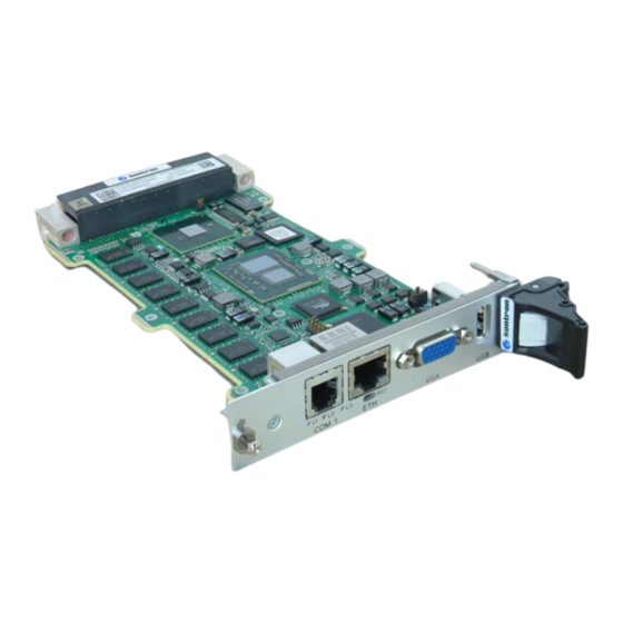
VX3030 User's Guide Physical I/O Chapter 4 - Physical I/O Front Panel Connectors Serial Graphics Figure 17: Location of the Front Panel Connectors CA.DT.A87-5e Page 35... -
Page 48: Serial Connector - Com
VX3030 User's Guide 4.1.1 Serial Connector - COM The VX3030 integrates two serial communications ports, COM1 and COM2 in PC parlance. COM1 and COM2 are available via the VPX P2 connector. COM1 is also available via the front panel connector. - Page 49 4 RJ-14 (6 pin, 4 conductor) for a simple EIA-232 without handshake support. 4 RJ-12 (6 pin, 6 conductor) for EIA-232 with handshaking. A RJ-12 to DB9/DB25 male or DB9/DB25 female adapter is available from multiple sources, such as: 4 Kontron Order Code KIT-2X-RJ12DB9 4 Triangle Cable http://www.trianglecables.com/db9m-rj12.html Pin Connector Pin Connec...
-
Page 50: Gigabit Ethernet Connectors
Physical I/O VX3030 User's Guide 4.1.2 Gigabit Ethernet Connectors The Ethernet transmission should operate using a CAT5 cable with a maximum length of 100 m. The Ethernet connectors are available as RJ-45 connectors with tab down. The interfaces provide automatic detection and switching between 10Base-T, 100Base-TX and 1000Base-T data transmission (Auto- Negotiation). -
Page 51: Usb Connector
VX3030 User's Guide Physical I/O 4.1.3 USB Connector Pin Assignment SIGNAL FUNCTION VCC (+5V Protected) VCC USB_D- Differential USB- USB_D+ Differential USB+ Figure 20: USB Connector Table 16: USB Connector Pin Assignment 4.1.4 VGA Connector Pin Assignment SIGNAL FUNCTION Red Video Signal Output... -
Page 52: Onboard Connectors
Physical I/O VX3030 User's Guide Onboard Connectors Figure 22: Onboard Connectors Page 40 CA.DT.A87-5e... -
Page 53: Table 18: Onboard Nand Flash Pin Assignment
The onboard USB device is used to connect an USB Flash Disk Module (low profile USB flash mezzanine card, 2 mm connector) or a SATA NAND flash module.. The following table provides pinout information for the onboard USB connector USB mezzanine slot: SIGNAL FUNCTION SATA VX3030 receive + Data- Differential USB- SATA VX3030 receive - Data+... -
Page 54: Rear Connectors
Physical I/O VX3030 User's Guide Rear Connectors VPX Bus Interface The complete 3U VPX connector configuration comprises three connectors named P0 to P2: > P0: 8-wafer 7-row connector. > P1 - P2: 16-wafer 7-row differential connectors. Figure 23: VPX Connectors Page 42 CA.DT.A87-5e... -
Page 55: P0 Connector
VX3030 User's Guide Physical I/O 4.3.1 P0 Connector P0 Wafer Assignment Wafer ROW G ROW F ROW E ROW D ROW C ROW B ROW A +12V +12V +12V +3V3 +3V3 +3V3 +12V +12V +12V +3V3 +3V3 +3V3 I2C1 CLK... -
Page 56: Table 20: Vpx Connector P0 Signal Definition
I2C1 I2C Bus 1 REF_CLK+/- The Reference Clock is a bussed differential pair. Output if the VX3030 is plugged in the system controller slot, input otherwise. It enables the entire system to synchronize to a common time reference if desired. -
Page 57: P1 Connector
VX3030 User's Guide Physical I/O 4.3.2 P1 Connector P1 Wafer Assignment > Legend for Table 21: P1_VBAT USB2/3 USB links 2 and 3 from PCH Battery Voltage P1_SYS_CON* System Controller SATA0/3 SATA links 0 and 3 from PCH P1_REFCLK0-SE Single ended Reference Clocks... -
Page 58: Table 22: Vpx Connector P1 Signal Definition
Physical I/O VX3030 User's Guide P1 Signal Definition MNEMONIC SIGNAL DEFINITION P1-REF_CLK_SE Reserved PCIe0 Lx-RX+/- x4 PCI Express Link. Receive +/- Can also be used as a 4 x1 links PCIe0 Lx-TX+/- x4 PCI Express Link. Transmit +/- Can also be used as a 4 x1 links. -
Page 59: P2 Connector
VX3030 User's Guide Physical I/O 4.3.3 P2 Connector P2 Wafer Assignment > Legend for Table 23: COM1/2 Simplified Serial Lines PCIe_TX/RX Additionnal PCI express x1 link from PCH USB4/5 USB links from PCH PCIe_CLK Additionnal PCI express clock from PCH... -
Page 60: Xdp
Physical I/O VX3030 User's Guide P2 Signal Definition MNEMONIC SIGNAL DEFINITION COMx Serial Lines, EIA-232/EIA-485 USBx PWR USB Power link x USBx D+/- Differential Data pair of USB link x SATAx RX+/- Serial ATA. Receive +/- link x SATAx TX+/- Serial ATA. -
Page 61: Leds
VX3030 User's Guide Physical I/O LEDs Status LEDs Default Setting There are three bicolor LEDs (Red/Green) on the front panel of the VX3030 3U VPX board. L1, L2, L3 Figure 24: LEDs Front panel CPU LED COLOR DESCRIPTION Permanent error on subsystem... -
Page 62: Chapter 5 - Power And Thermal Specifications
Does not include current eventually supplied to external periphals like USB. Board Thermal Monitoring To ensure optimal and long-term reliability of the VX3030, all onboard components must remain within the maximum temperature specifications. The most critical components on the VX3030 are the processor and the memory. -
Page 63: Figure 25: Board Temperature Sensors Location
VX3030 User's Guide Power and Thermal Specifications Location of the Temperature Sensors Board Sensor Figure 25: Board Temperature Sensors Location CA.DT.A87-5e Page 51... -
Page 64: Cpu Thermal Monitoring
For instance, for: > a VX3030 (Order Code: VX3030-SA22-00000) at 55°C for a frequency CPU Max. of 2 GHz, the minimum air flow needed to cool enough the processor die is about 12 CFM (either 2.8 m/s) in a 0.8 inch slot. - Page 65 Learn more about Intel Turbo Boost Technology: http://www.intel.com/technology/turboboost/ > The Intel Turbo Boost is handled by the BIOS through the CPU configuration menu. Refer to the AMI BIOS for VX3030 - User Reference Manual (SD.DT..), section “CPU Configuration”. CA.DT.A87-5e Page 53...
-
Page 66: Chapter 6 - Backplane Suggestions
Backplane Suggestions VX3030 User's Guide Chapter 6 - Backplane Suggestions Kontron can offer for development or deployement of the VX3030 the following backplane models: Single Star x4 Figure 27: Single Star x4 Topology Page 54 CA.DT.A87-5e... -
Page 67: Figure 28: Dual Star X4 Topology
VX3030 User's Guide Backplane Suggestions Dual Star x4 Figure 28: Dual Star x4 Topology CA.DT.A87-5e Page 55... -
Page 68: Figure 29: Single Star X2 Topology
Backplane Suggestions VX3030 User's Guide Single Star x2 Figure 29: Single Star x2 Topology Page 56 CA.DT.A87-5e... -
Page 69: Chapter 7 - Vx3030-Rtm Characteristics
Rear I/O connector J2 on the VX3030. When the VX3030-RTM is used, the signals of some of the main board/front panel connectors are routed to the module interface. Thus, the VX3030 Rear Transition Module makes it much easier to remove the CPU in the rack as there is practically no cabling on the CPU board. -
Page 70: Technical Specifications
One USB interface used to connect a Flash disk I2C Bus JTAG Temperature Range Operational: 0_C to +55_C Storage: -55_C to +85_C Climatic Humidity 99% non-condensing General Dimensions Dimensions: 99.85 mm x 82.54 mm Board Weight 120g Table 27: VX3030-RTM Main Specifications Page 58 CA.DT.A87-5e... -
Page 71: Rtm Configuration
VX3030 User's Guide VX3030-RTM Characteristics RTM Configuration Figure 31: VX3030-RTM MicroSwitch Location MicroSwitch SW2 Function Description NVMRO Set NVMRO VPX signal to Ground Non-Volatile Memory Read Only No action on NVMRO VPX signal Default setting Reserved Reserved COM1 Differential Termination Connect a 100 Ohms parallel termi... -
Page 72: Connectors
VX3030-RTM Characteristics VX3030 User's Guide Connectors 7.4.1 RTM Connectors Identification Alignment/Keying Pins Alignment/Keying Sockets Figure 32: Connector Identification for 3U RTM Page 60 CA.DT.A87-5e... -
Page 73: Front Panel Connectors
Front Panel Connectors ETH1 ETH0 Gigabit Ethernet SERIAL USB 2.0 CN12−R CN13−R CN10−R CN11−R Reset Button Figure 33: VX3030-RTM Front Panel Connectors LED 1 to LED 5 are not connected. ETH0 Gigabit Ethernet CN12-R is not used CA.DT.A87-5e Page 61... -
Page 74: Onboard Connectors
CN20−R COM2 SATA1 SATA2 SERIAL CN14−R CN15−R CN19−R GPIO CN17−R USB 2.0 CN21−R JTAG CN18−R COM1 ETH0 ETH1 USB 2.0 SERIAL Gigabit Ethernet CN11−R CN10−R CN12−R CN13−R Figure 34: VX3030-RTM Onboard Connectors SATA3 CN16-R is not used Page 62 CA.DT.A87-5e... - Page 75 VX3030 User's Guide VX3030-RTM Characteristics CN10-R, CN19-R See section 7.5.1 "COM Interfaces" page 64 CN11-R, CN21-R See section 7.5.2 "USB Interfaces" page 65 CN13-R See section 7.5.3 "Gigabit Ethernet Interfaces" page 68 CN14-R, CN15-R See section 7.5.4 "Serial ATA Interfaces"...
-
Page 76: Modules Interfaces
VX3030 User's Guide Modules Interfaces 7.5.1 COM Interfaces The VX3030-RTM provides two COM (COM1 and COM2) ports for connecting devices to the VX3030-RTM. > COM1 serial port RJ-12 connector is located on the front panel of the RTM. > COM2 serial port RJ-12 connector is located onboard. -
Page 77: Usb Interfaces
7.5.2 USB Interfaces There are two USB 2.0 ports available on the VX3030-RTM, each with a maximum transfer rate of 480 Mb/s provided for connecting USB devices. > One interface is available on the VX3030-RTM front panel. One USB peripheral may be connected to this port. -
Page 78: Table 31: Onboard Usb Connector Pinout
Table 31: Onboard USB Connector Pinout The USB Flash module is fixed to the board, by using on one side the CN21-R connector, and on the other side, a standoff screwed to the VX3030-RTM board and to the USB Flash module. to standoff to CN21−R... - Page 79 VX3030 User's Guide VX3030-RTM Characteristics USB Flash Disk Layout: 4 The maximum space reserved for the USB flash disk is 36.9 mm x 26.6 mm (LxW) 4 The distance between the connector and the screw hole is 27.3 mm~27.9mm 4 The maximum allowable connector height is 3.68 mm Figure 40: USB Flash Disk Layout CA.DT.A87-5e...
-
Page 80: Gigabit Ethernet Interfaces
VX3030-RTM Characteristics VX3030 User's Guide 7.5.3 Gigabit Ethernet Interfaces The Ethernet connector is a RJ-45 connector. The interfaces provide automatic detection and switching between 10BASE-T, 100BASE-TX and 1000BASE-T data transmission (Auto-Negotiation). Auto-wire switching for crossed cables is also supported (Auto-MDI/X). -
Page 81: Serial Ata Interfaces
Table 33: Onboard SATA Connectors Pinout When using a Serial ATA cable, it is recommended to use a special right-angled Serial ATA cable due to possible space limitations within the system. For further information, contact Kontron's Technical Support. SATA3 CN16-R is not used. -
Page 82: Gpio Connector
Reserved Ground Ground Reserved Reserved GPIO1(*) General Purpose IO Ground GPIO2 General Purpose IO CN17−R Ground (*) Signals available when RTM is connected to VX3030 product Table 34: Onboard GPIO Connector Pinout Figure 43: Onboard GPIO Connector Page 70 CA.DT.A87-5e... -
Page 83: Jtag Connector
General Purpose IO N.C. Not Connected N.C. Not Connected GPIO4 (*) General Purpose IO CN18−R Reserved Ground (*) Signals available when RTM is connected to VX3030 product Figure 44: Onboard JTAG Connector Table 35: Onboard JTAG Connector Pinout CA.DT.A87-5e Page 71... -
Page 84: I2C System Management Connector
VX3030-RTM Characteristics VX3030 User's Guide 7.5.7 I2C System Management Connector Routed from RP0 to CN20-R connector (right angle HE10 10-pin connector male). SIGNAL DESCRIPTION SMB0 CLK SM Bus 0 Serial Clock SMB1 CLK SM Bus 1 Seria Clock Ground Ground... -
Page 85: Reset
The VX3030-RTM generates a system reset signal on the VPX bus at each +5V power-on for a duration of 140 ms to 560 ms. In addition, the front panel reset push button of the VX3030-RTM is used to generate a VPX bus reset with the same minimum duration. -
Page 86: Rear I/O Interfaces
VX3030-RTM Characteristics VX3030 User's Guide Rear I/O Interfaces The VX3030 Rear Transition Module conducts a wide range of I/O signals through the Rear I/O connectors RP0, RP1 and RP2. > RP0: one 15-wafer 7-row connector > RP1: one 16-wafer 7-row connector >... -
Page 87: Rp2 Connector
VX3030 User's Guide VX3030-RTM Characteristics 7.8.1 RP2 Connector > Legend for Table 37 COM1/2 Simplified Serial Lines PCIe_CLK Additionnal PCI express clock from PCH PCIe_TX/RX Additionnal PCI express x1 link from PCH eDP-A/B Digital ports A and B from PCH... -
Page 88: Rp1 Connector
VX3030-RTM Characteristics VX3030 User's Guide 7.8.2 RP1 Connector RP1 Wafer Assignment > Legend for Table 39 USB2/3 USB links 2 and 3 from PCH SATA0/3 SATA links 0 and 3 from PCH ETHx TX/RX 1000BASE-BX links 0 and 1 from Dual... - Page 89 VX3030 User's Guide VX3030-RTM Characteristics RP1 Signal Definition Mnemonic Signal Definition SATAx RX+/- Serial ATA. Receive +/- link x SATAx TX+/- Serial ATA. Transmit +/- link x USBx PWR USB Power link x USBx D+/- Differential Data pair of USB link x ETH DA+/- Ethernet 1000BASE-T: First pair of transmit/receive data.
-
Page 90: Rp0 Connector
VX3030-RTM Characteristics VX3030 User's Guide 7.8.3 RP0 Connector RP0 Wafer Assignment Board Row G Row F Row E Row D Row C Row B Row A Wafer Wafer N.C. N.C. N.C. N.C. N.C. N.C. N.C. P0 w02 P0 w03 Reserved... -
Page 91: Pci 64 Pim Connector
VX3030 User's Guide VX3030-RTM Characteristics PCI 64 PIM Connector 7.9.1 J14 Connector J14 Connector Pin Assignment Signal Signal SATA1 TX- eDP-B 3- SATA1 RX- eDP-B2- SATA1 TX+ eDP-B 3+ SATA1 RX+ eDP-B 2+ SATA2 TX- PCIe CLK- SATA2 RX- eDP-B AUX-... - Page 92 VX3030-RTM Characteristics VX3030 User's Guide Signal Description Mnemonic Description eDPx embedded Display Port PCIe1 TX/RX Additional PCI-Express x1 link PCIe1 CLK Common Reference Clock Output for PCIe1 SATAx RX+/- Serial ATA. Receive +/- link x SATAx TX+/- Serial ATA. Transmit +/- link x...
-
Page 93: J10 Connector
VX3030 User's Guide VX3030-RTM Characteristics 7.9.2 J10 Connector J10 Connector Pin Assignment Signal Signal Signal Signal N.C. +12V_AUX N.C. N.C. N.C. N.C. N.C. N.C. +3.3V N.C. N.C. N.C. N.C. N.C. N.C. N.C. N.C. N.C. N.C. N.C. N.C. +3.3V N.C. N.C. -
Page 94: Chapter 8 - Vx3030-Rc Characteristics
Rugged conduction-cooled 3U VPX Single Board Computer, 2 GHz VX3030-RC VX3030-RC24-0N000 Intel® Core™ i7, 4 GB DDR3-SDRAM Rugged conduction-cooled 3U VPX Single Board Computer, 2 GHz VX3030-RC VX3030-RC28-0N000 Intel® Core™ i7, 8 GB DDR3-SDRAM Table 43: VX3030-RC Order Code Page 82 CA.DT.A87-5e... -
Page 95: Vx3030-Rc Specificities
MTBF depends on the environmental class Section 8.4 page 85 Section 1.6 page 15 Section 8.5 page 86 Peripheral Connectivity No connector available on the board front panel Mezzanine Installation Section 8.6 page 87 Table 44: VX3030-RC Specificities CA.DT.A87-5e Page 83... -
Page 96: Board Identification
Board Identification The VX3030-RC boards are identified by labels fitted on top and bottom sides. These labels are at the same location and have the same meaning as the VX3030-SA boards (refer to section 2.2 “Board Identification” page 18). In addition, the ruggedizer is identified by: “Ruggedizer Identification”... -
Page 97: Environmental Specifications
AIC (Hours) NS (Hours) ARW (Hours) 25°C 40°C 40°C 25°C 40°C 55°C MTBF (hours) 479 633 h 350 811 h 68 202 h 97 285 h 78 329 h 16 765 h Table 46: VX3030-RC22-0N000 MTBF Data CA.DT.A87-5e Page 85... -
Page 98: Peripheral Connectivity
VX3030-RC Characteristics VX3030 User's Guide Peripheral Connectivity VX3030-RC FUNCTION Front Panel Onboard Gigabit Ethernet Y (Flash module) SATA Y (Flash module) COM1 -(EIA-232/485) COM2 - (EIA-232 /485) Reset Button Table 47: Peripheral Connectivity Page 86 CA.DT.A87-5e... -
Page 99: Mezzanine Installation
The USB or SATA Flash module is fixed to the board, by using on one side the USB/SATA connector, and on the other side, a nylon screw mounted on the VX3030 heatsink. Refer to section 2.7.1 page 25 for more information. -
Page 100: Thermal Performance
JMAX For instance, for: > a VX3030 (Order Code: VX3030-RC22-00000) with core frequency at 2 Ghz, the maximum wedge lock temperature allowed to cool enough the processor die without entering throttling mode is about 80.5°C. > a VX3030 (Order Code: VX3030-RC22-00000) with core frequency at 1.733Ghz, the maximum wedge lock temperature allowed to cool enough the processor die without entering throttling mode is about 85°C. - Page 101 Kontron Modular Computers S.A.S. +33 (0) 4 98 16 34 00 150 rue Marcelin Berthelot - BP 244 sales@kontron.com ZI TOULON EST support-kom-sa@kontron.com 83078 TOULON CEDEX - France For further information about other Kontron products, please visit our Internet web site: www.kontron.com.
Need help?
Do you have a question about the VX3030 and is the answer not in the manual?
Questions and answers