Table of Contents
Advertisement
Quick Links
UM11854
KITPF5030SKTEVM programming board
Rev. 1 — 9 March 2023
Document information
Information
Keywords
Abstract
Content
PF5030, KITPF5030SKTEVM, KL25Z, I
The KITPF5030SKTEVM provides flexibility to explore all the features of the device and make
measurements on the main part of the application.
2
C, spf-53091
User manual
Advertisement
Table of Contents

Subscribe to Our Youtube Channel
Related Manuals for NXP Semiconductors KITPF5030SKTEVM


Summary of Contents for NXP Semiconductors KITPF5030SKTEVM
- Page 1 Rev. 1 — 9 March 2023 User manual Document information Information Content Keywords PF5030, KITPF5030SKTEVM, KL25Z, I C, spf-53091 Abstract The KITPF5030SKTEVM provides flexibility to explore all the features of the device and make measurements on the main part of the application.
- Page 2 UM11854 NXP Semiconductors KITPF5030SKTEVM programming board Revision history Date Description 20230309 Initial release UM11854 All information provided in this document is subject to legal disclaimers. © 2023 NXP B.V. All rights reserved. User manual Rev. 1 — 9 March 2023...
- Page 3 UM11854 NXP Semiconductors KITPF5030SKTEVM programming board Important notice NXP provides the enclosed product(s) under the following conditions: This evaluation kit is intended for use of ENGINEERING DEVELOPMENT OR EVALUATION PURPOSES ONLY. It is provided as a sample IC pre-soldered to a printed circuit board to make it easier to access inputs, outputs, and supply terminals.
-
Page 4: Introduction
PF5030 Configurable Power Management IC. The KITPF5030SKTEVM enables development on PF5030 family of devices. The kit can be connected to the NXP GUI software, which allows the user to explore registers, try OTP configurations, and burn the part. -
Page 5: Finding Resources And Information On The Nxp Website
NXP Semiconductors KITPF5030SKTEVM programming board 2 Finding resources and information on the NXP website NXP Semiconductors provides online resources for this evaluation board and its supported devices on http:// www.nxp.com. The information page for KITPF5030SKTEVM board is available at http://www.nxp.com/KITPF5030SKTEVM. -
Page 6: Getting Ready
NXP Semiconductors KITPF5030SKTEVM programming board 3 Getting ready Working with the KITPF5030SKTEVM requires the kit contents, additional hardware, and a Windows PC workstation with installed software. 3.1 Kit contents • Assembled and tested KITPF5030SKTEVM connected to a FRDM-KL25Z in an anti-static bag •... -
Page 7: Getting To Know The Hardware
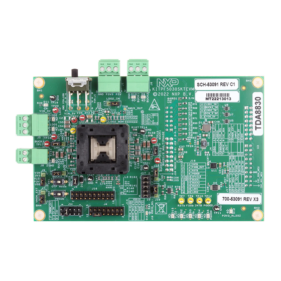
KITPF5030SKTEVM programming board 4 Getting to know the hardware The KITPF5030SKTEVM provides flexibility to explore all the features of the device and make measurements on the main part of the application. In combination with the FRDM-KL25Z MCU board, the NXP GUI software allows access to the registers in read and write mode. -
Page 8: Schematic, Board Layout, And Bill Of Materials
UM11854 NXP Semiconductors KITPF5030SKTEVM programming board 4.3 Schematic, board layout, and bill of materials The schematic, board layout, and bill of materials for the KITPF5030SKTEVM board are available at http:// www.nxp.com/KITPF5030SKTEVM. 4.3.1 VMON board configuration The VMON configuration is highly dependent on the use case. This kit is delivered with a default configuration. -
Page 9: I2C
C bus on J4 connector, but J17 1-2 and 3-4 must be removed to disconnect the FRDM-KL25Z MCU (see Figure 3). In addition to this change, make sure that the VDDIO voltage domain and ground are the same on MCU side and KITPF5030SKTEVM side. I2C_SCL_SH 3 I2C_SCL... -
Page 10: Vddio
UM11854 NXP Semiconductors KITPF5030SKTEVM programming board 4.3.3 VDDIO The VDDIO pin is powered through VDDIO net and is used to supply internal buffers and I C communication. The selection of VDDIO is made using J14 connector as shown in Figure 4. -
Page 11: Kit Featured Components
UM11854 NXP Semiconductors KITPF5030SKTEVM programming board 4.4 Kit featured components Figure 6 identifies important components and Table 1 provides details. Figure 6. Evaluation board featured components location Table 1. Evaluation board featured components location Number Description VIN_5V and VIN_3V3 power supply input VIN three position switch •... - Page 12 UM11854 NXP Semiconductors KITPF5030SKTEVM programming board Table 1. Evaluation board featured components location ...continued Number Description PWRON pin switch Signal debug connector FRDM-KL25Z board signals connection FRDM-KL25Z board connectors VLED supply configuration UM11854 All information provided in this document is subject to legal disclaimers.
-
Page 13: Connectors
UM11854 NXP Semiconductors KITPF5030SKTEVM programming board 4.4.1 Connectors Figure 7 shows the location of connectors on the board. Figure 7. Evaluation board connectors location 4.4.1.1 VIN connector (J1) Table 2. VIN_5V and VIN_3V3 connector (J1) Schematic label Signal name Description J1-1 VIN_5V... -
Page 14: Debug Connector (J4)
UM11854 NXP Semiconductors KITPF5030SKTEVM programming board Table 4. BUCK1/2 connector (J6) Schematic label Signal name Description J6-1 BUCK2 BUCK2 regulator output J6-2 BUCK1 BUCK1 regulator output J6-3 Ground Table 5. BUCK3 connector (J8) Schematic label Signal name Description J8-1 BUCK3 BUCK3 regulator output... -
Page 15: Frdm-Kl25Z Board Connectors
UM11854 NXP Semiconductors KITPF5030SKTEVM programming board Table 7. Voltage monitoring connector (J16) ...continued Schematic label Signal name Description J16-5 Ground J16-6 RSTB Reset input / output pin (active low-logic level) J16-7 Ground J16-8 PGOOD Power good output pin J16-9 Ground J16-10... - Page 16 UM11854 NXP Semiconductors KITPF5030SKTEVM programming board Table 10. FRDM-KL25Z ADC connector (J10) Schematic label Signal name Description J10-1 BUCK2_ADC BUCK2 regulator output to KL25Z ADC J10-2 DBG_ADC DBG pin voltage to KL25Z ADC J10-3 BUCK1_ADC BUCK1 regulator output to KL25Z ADC...
-
Page 17: Test Points
UM11854 NXP Semiconductors KITPF5030SKTEVM programming board 4.4.2 Test points Figure 8 shows test points that provide access to various signals to and from the boards. Figure 8. Evaluation board test points Table 13. Evaluation board test points description Test point name Signal name... -
Page 18: Jumpers
UM11854 NXP Semiconductors KITPF5030SKTEVM programming board 4.4.3 Jumpers Figure 9 shows jumper locations for board configuration. Figure 9. Evaluation board jumpers location (with default position) Table 14. Evaluation board jumpers description Name Function Pin number Description Apply voltage to DBG pin 1–2 Either 4.5 V (DBG mode) or 7.95 V (OTP mode). - Page 19 UM11854 NXP Semiconductors KITPF5030SKTEVM programming board Table 14. Evaluation board jumpers description ...continued Name Function Pin number Description VDDIO input 1−2 VDDIO tied to LDO1 VDDIO tied to LDO2 VDDIO tied to VDDIO_EXT VDDIO tied to VDDIO_SEL 9-10 VDDIO tied to VIN_3V3 BUCK1/2 multiphase 1−2...
-
Page 20: Led Signaling
UM11854 NXP Semiconductors KITPF5030SKTEVM programming board 4.4.4 LED signaling Figure 10 shows the LEDs provided as visual output devices for the evaluation board: Figure 10. Evaluation board LED signaling location Table 15. Evaluation board LED signaling description Label Name Color Description RSTB... -
Page 21: Switches
UM11854 NXP Semiconductors KITPF5030SKTEVM programming board 4.4.5 Switches Figure 11 Figure 12 show switches locations for board operation. Figure 11. Switches location top UM11854 All information provided in this document is subject to legal disclaimers. © 2023 NXP B.V. All rights reserved. - Page 22 UM11854 NXP Semiconductors KITPF5030SKTEVM programming board Figure 12. Switches location bottom Table 16. SW1 description Position Function Description PF5030 OTP can be emulated and programmed when J3 RIGHT OTP mode ON populated LEFT OTP mode OFF PF5030 OTP cannot be emulated and programmed Table 17. SW2 description...
- Page 23 UM11854 NXP Semiconductors KITPF5030SKTEVM programming board Table 18. SW3 description Switch number Line Description VIN_5V BUCK1 Each LED is connected through an independent switch. BUCK2 Disconnecting them allows more accurate efficiency measurement. BUCK3 The switches also disconnect the FRDM-KL25Z ADC inputs.
-
Page 24: Installing And Configuring Software And Tools
UM11854 NXP Semiconductors KITPF5030SKTEVM programming board 5 Installing and configuring software and tools The programming/evaluation boards are always delivered with the GUI firmware already flashed. If MCU firmware is already flashed, ignore this section. If it is specified that firmware must be updated or it is malfunctioning, follow these instructions. -
Page 25: Installing Nxp Gui Software Package
UM11854 NXP Semiconductors KITPF5030SKTEVM programming board 5.2 Installing NXP GUI software package To install the "NXP GUI for Automotive PMIC Families" or obtain the NXP GUI package, unzip an open "1 - NXP_GUI_Setup" folder as shown in Figure Figure 15. NXP_GUI_Setup folder Then double click on the "NXP_GUI-version-Setup.exe"... - Page 26 UM11854 NXP Semiconductors KITPF5030SKTEVM programming board Figure 18. NXP GUI setup 2/2 Select the options shown in Figure 19 before completing the installation of the setup: • Run NXP_GUI • Show Readme Figure 19. NXP GUI setup completion Select Finish to complete the installation.
-
Page 27: Using Pf5030 Nxp Gui
UM11854 NXP Semiconductors KITPF5030SKTEVM programming board 6 Using PF5030 NXP GUI To follow the steps in this section, ensure that the board is connected using the appropriate hardware configuration. Always use the latest version of the NXP GUI. 6.1 Starting the PF5030 NXP GUI When your kit is ready and the NXP GUI is installed, click to launch the GUI from your Windows search bar. -
Page 28: Power Tab
UM11854 NXP Semiconductors KITPF5030SKTEVM programming board Figure 21. NXP GUI framework You are now using the PF5030 GUI interface. It can be divided in several parts: • Settings: Import or export files, configure framework. • Device Manager: Start communication with device. Enter or exit test mode. I C communication settings. -
Page 29: Otp Tab
UM11854 NXP Semiconductors KITPF5030SKTEVM programming board Figure 22. NXP GUI framework - POWER tab Each regulator can be enabled / disabled by clicking on the upper left corner check box. Additional options are available on the menu on the upper right corner of each regulation, such as: •... -
Page 30: System Configuration Tab
UM11854 NXP Semiconductors KITPF5030SKTEVM programming board These tabs are used to define the entire PF5030 OTP configuration. When the OTP configuration is defined, TBB/OTP scripts can be generated using the Export menu. Generate a TBB file for emulation and an OTP file for OTP programming. -
Page 31: Switching And Ldo Regulators Tab
UM11854 NXP Semiconductors KITPF5030SKTEVM programming board Figure 24. OTP System Configuration tab, part 2 of 2: Power-up sequence diagram 6.3.2 Switching and LDO regulators tab The switching and LDO Regulators tab shown in Figure 25 has several sections: • Block diagram: Summarizes the output voltage and startup slot of each regulator •... -
Page 32: Establishing The Connection Between The Nxp Gui And The Hardware
UM11854 NXP Semiconductors KITPF5030SKTEVM programming board Figure 26. OTP Functional Safety tab 6.4 Establishing the connection between the NXP GUI and the hardware The device manager allows the connection of the PF5030 development board with the NXP GUI. Before plugging the KL25Z USB port to the computer, the MCU is in a “NOT DETECTED” state. -
Page 33: Otp Mode And Device Programming
UM11854 NXP Semiconductors KITPF5030SKTEVM programming board commands to the main state and the fail-safe state machine to exit OTP mode and initiate device start-up. The addresses are automatically updated to keep device communication. Test mode can be enabled and disabled by clicking the Test Mode button when DBG pin voltage is 7.95 V (EVB OTP mode LED on). - Page 34 UM11854 NXP Semiconductors KITPF5030SKTEVM programming board Figure 28. Device programming To set up the hardware before OTP burning, see Section 7.3 configure put device in OTP mode, then follow the steps: • Start the device in OTP mode. • Enter Test mode.
-
Page 35: User Mode Controls
UM11854 NXP Semiconductors KITPF5030SKTEVM programming board To check if a valid OTP configuration is already burned, switch off the supply and then on again. Start the device by clicking the "Exit OTP Mode" button. The device starts with the OTP configuration. -
Page 36: Management Commands
UM11854 NXP Semiconductors KITPF5030SKTEVM programming board Figure 30. Script editor Help window 6.6.1.2 Management commands Some commands are used for formatting the scripts. Figure 31 shows the description of each button. Figure 31. Script editor commands • Run: Runs the script once. -
Page 37: Script Generator
UM11854 NXP Semiconductors KITPF5030SKTEVM programming board 6.6.1.3 Script generator The script editor allows the user to save script sequence files, as shown in Figure 32. However, a script sequence file is already saved as an example in the script generator. This script is used to release FS0B when the PF5030 is using simple watchdog. - Page 38 UM11854 NXP Semiconductors KITPF5030SKTEVM programming board Figure 33. Main mirrors tab Figure 34. Fail-safe mirrors tab UM11854 All information provided in this document is subject to legal disclaimers. © 2023 NXP B.V. All rights reserved. User manual Rev. 1 — 9 March 2023...
-
Page 39: Access Tab
UM11854 NXP Semiconductors KITPF5030SKTEVM programming board 6.6.3 Access tab 6.6.3.1 Register map All PF5030 I C registers can be accessed in write and read mode using this tab shown in Figure 35. These registers are divided into three sections: • Functional: Main functional I C registers (diagnostics, configuration, and controls) •... -
Page 40: Init Safety Tab
UM11854 NXP Semiconductors KITPF5030SKTEVM programming board Figure 36. Bitmap dialog Writing an INIT_FS register automatically updates the corresponding NOT register. 6.6.3.2 INIT Safety tab This tab allows the initialization phase (INIT_FS state) configuration, that must be done before the first good watchdog refresh until the 2 seconds timeout limit. -
Page 41: Watchdog Tab
UM11854 NXP Semiconductors KITPF5030SKTEVM programming board Figure 37. INIT safety tab To ease the configuration, Read and Write All buttons are implemented. 6.6.3.3 Watchdog tab The watchdog tab gathers all the registers and configurations having an impact on the watchdog, except "Watchdog Type". -
Page 42: Diagnostic Safety Tab
UM11854 NXP Semiconductors KITPF5030SKTEVM programming board Figure 38. Watchdog tab 6.6.3.4 Diagnostic Safety tab The diagnostic safety tab shown in Figure 39 makes it possible to know the safety status of the device. The safety function events, like voltage monitoring flags, analog and logical BIST status, and safety pins are automatically reported in this tab. -
Page 43: Regulators Tab
UM11854 NXP Semiconductors KITPF5030SKTEVM programming board The PF5030 can enter STANDBY/LPOFF state using the "Go to Standby" command, setting the bit GOTO_STBY = 1. Figure 40. Main tab 6.6.3.6 Regulators tab The regulator tab shown in Figure 41 is used to configure the PF5030 SMPS or LDO. Regulators can be enabled or disabled on registers using I C commands, and the state / status of each regulators is also shown. -
Page 44: Main Interrupts Tab
UM11854 NXP Semiconductors KITPF5030SKTEVM programming board 6.6.3.7 Main interrupts tab The main interrupts tab shown in Figure 42 allows the monitoring of the regulators, the wake inputs, and the communication events or status. It allows the reading, writing, and polling of overvoltage/undervoltage, overtemperature, and overcurrent flags. -
Page 45: Fail-Safe Interrupts Tab
UM11854 NXP Semiconductors KITPF5030SKTEVM programming board 6.6.3.8 Fail-safe interrupts tab The fail-safe interrupts tab shown in Figure 43 allows the monitoring of the overvoltage/undervoltage fail-safe monitoring status and the watchdog. It allows the reading, writing, and polling of overvoltage/undervoltage flags. -
Page 46: Amux
UM11854 NXP Semiconductors KITPF5030SKTEVM programming board 6.6.3.9 AMUX The AMUX tab shown in Figure 44 allows the selection of an AMUX pin channel and gets its current value by using the exclusive KL25Z AMUX ADC channel. You can do a single read or display various channels dynamically on the voltage or temperature graph. -
Page 47: Using An Evaluation Board
UM11854 NXP Semiconductors KITPF5030SKTEVM programming board 7 Using an evaluation board Before starting the process, consult the development board scheme and user manual to configure the required use case. Learn about OTP before operating with the device. The device has a high level of flexibility due to the parameter configuration available in the OTP. -
Page 48: Configuring The Hardware For Start-Up
UM11854 NXP Semiconductors KITPF5030SKTEVM programming board OTP mode activation implies in Debug mode activation. Debug and OTP modes can be disabled with an I C command. Test mode can be enabled at any moment with an I C command when the voltage is applied on DBG pin. -
Page 49: Working In Otp Emulation Mode
Close (OTP mode ON) 2. Connect the Windows PC USB port to the KITPF5030SKTEVM board using the provided USB 2.0 cable. 3. If external power supplies are used, set the power supplies to 3.3 V and 5.0 V, and current limit to 1.0 A. -
Page 50: Releasing Fs0B Script
UM11854 NXP Semiconductors KITPF5030SKTEVM programming board c. Otherwise, the mirror registers are not filled and the OTP fuse is not burned. The device does not start up properly. Device is in Debug mode. As long as Debug mode is not exited by writing FS_STATES: [FS_DBG_MODE_EXIT] bit to 1, the FS0B pin cannot be released. -
Page 51: References
UM11854 NXP Semiconductors KITPF5030SKTEVM programming board 8 References KITPF5030SKTEVM — detailed information on this board, including documentation, downloads, and software and tools http://www.nxp.com/KITPF5030SKTEVM PF5030 — detailed information on PF5030 http://www.nxp.com/PF5030 NXP GUI for Automotive PMIC Families — Software GUI for NXP Automotive PMIC products https://www.nxp.com/PMIC-GUI-SW... -
Page 52: Legal Information
NXP Semiconductors. In no event shall NXP Semiconductors be liable for any indirect, incidental, Evaluation products — This product is provided on an “as is” and “with all punitive, special or consequential damages (including - without limitation - faults”... - Page 53 UM11854 NXP Semiconductors KITPF5030SKTEVM programming board NXP — wordmark and logo are trademarks of NXP B.V. 9.3 Trademarks Notice: All referenced brands, product names, service names, and trademarks are the property of their respective owners. UM11854 All information provided in this document is subject to legal disclaimers.
- Page 54 UM11854 NXP Semiconductors KITPF5030SKTEVM programming board Tables Tab. 1. Evaluation board featured components Tab. 13. Evaluation board test points description ..17 location ............11 Tab. 14. Evaluation board jumpers description ..... 18 Tab. 2. VIN_5V and VIN_3V3 connector (J1) ....13 Tab.
- Page 55 UM11854 NXP Semiconductors KITPF5030SKTEVM programming board Figures Fig. 1. VMON_EXT assignment (VIN_3V3 default) ..8 Fig. 24. OTP System Configuration tab, part 2 of 2: Fig. 2. LDO1_MON and LDO2_MON input Power-up sequence diagram ......31 configuration ............8 Fig. 25.
-
Page 56: Table Of Contents
Getting to know the hardware ......7 Device modes ..........47 Kit overview ............7 Configuring the hardware for start-up ....48 KITPF5030SKTEVM features ......7 Working in OTP emulation mode .....49 Schematic, board layout, and bill of Releasing FS0B script ........50 References ............
Need help?
Do you have a question about the KITPF5030SKTEVM and is the answer not in the manual?
Questions and answers