Table of Contents
Advertisement
Quick Links
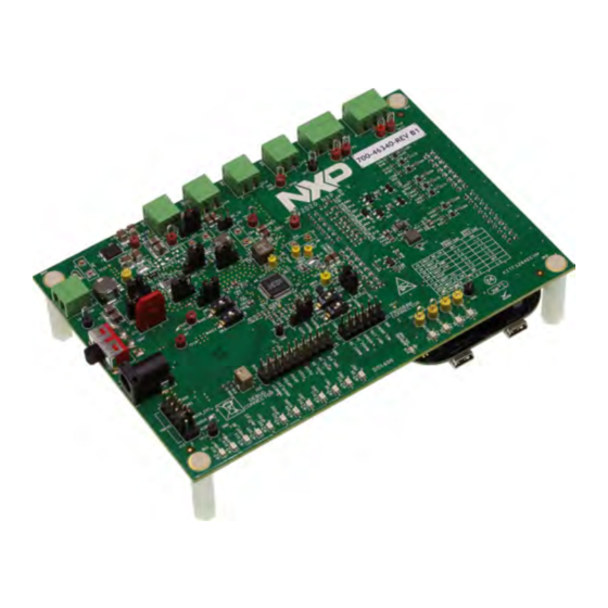
Figure 1. KITFS26AEEVM
Important Notice
NXP provides the enclosed product(s) under the following conditions:
This evaluation kit is intended for use of ENGINEERING DEVELOPMENT OR EVALUATION PURPOSES ONLY. It is provided as a
sample IC pre-soldered to a printed circuit board to make it easier to access inputs, outputs, and supply terminals. This evaluation board
may be used with any development system or other source of I/O signals by simply connecting it to the host MCU or computer board via
off-the-shelf cables. This evaluation board is not a Reference Design and is not intended to represent a final design recommendation for
any particular application. Final device in an application will be heavily dependent on proper printed circuit board layout and heat sinking
design as well as attention to supply filtering, transient suppression, and I/O signal quality.
The goods provided may not be complete in terms of required design, marketing, and or manufacturing related protective considerations,
including product safety measures typically found in the end product incorporating the goods. Due to the open construction of the product,
it is the user's responsibility to take any and all appropriate precautions with regard to electrostatic discharge. In order to minimize risks
associated with the customers applications, adequate design and operating safeguards must be provided by the customer to minimize
inherent or procedural hazards. For any safety concerns, contact NXP sales and technical support services.
Should this evaluation kit not meet the specifications indicated in the kit, it may be returned within 30 days from the date of delivery and will
be replaced by a new kit.
NXP reserves the right to make changes without further notice to any products herein. NXP makes no warranty, representation or
guarantee regarding the suitability of its products for any particular purpose, nor does NXP assume any liability arising out of the
application or use of any product or circuit, and specifically disclaims any and all liability, including without limitation consequential or
incidental damages. Typical parameters can and do vary in different applications and actual performance may vary over time. All operating
parameters, including Typical, must be validated for each customer application by customer's technical experts.
NXP does not convey any license under its patent rights nor the rights of others. NXP products are not designed, intended, or authorized
for use as components in systems intended for surgical implant into the body, or other applications intended to support or sustain life, or for
any other application in which the failure of the NXP product could create a situation where personal injury or death may occur.
Should the Buyer purchase or use NXP products for any such unintended or unauthorized application, the Buyer shall indemnify and hold
NXP and its officers, employees, subsidiaries, affiliates, and distributors harmless against all claims, costs, damages, and expenses, and
reasonable attorney fees arising out of, directly or indirectly, any claim of personal injury or death associated with such unintended or
unauthorized use, even if such claim alleges NXP was negligent regarding the design or manufacture of the part.
UM11503
KITFS26AEEVM evaluation board
Rev. 1 — 29 January 2021
User manual
Advertisement
Table of Contents

Related Manuals for NXP Semiconductors KITFS26AEEVM


Summary of Contents for NXP Semiconductors KITFS26AEEVM
- Page 1 UM11503 KITFS26AEEVM evaluation board Rev. 1 — 29 January 2021 User manual Figure 1. KITFS26AEEVM Important Notice NXP provides the enclosed product(s) under the following conditions: This evaluation kit is intended for use of ENGINEERING DEVELOPMENT OR EVALUATION PURPOSES ONLY. It is provided as a sample IC pre-soldered to a printed circuit board to make it easier to access inputs, outputs, and supply terminals.
-
Page 2: Introduction
The NXP community is at http://community.nxp.com. Getting ready Working with the KITFS26AEEVM requires the kit contents, additional hardware and a Windows PC workstation with installed software. 3.1 Kit contents • Assembled and tested evaluation board and preprogrammed FRDM-KL25Z microcontroller board in an anti-static bag •... -
Page 3: Windows Pc Workstation
• NXP GUI installation package Getting to know the hardware The KITFS26AEEVM provides flexibility to play with all the features of the device and make measurements on the main part of the application. The FRDM-KL25Z connected to the board, combined with the FS26 NXP GUI software allows full configuration and control of the FS26 SBC. -
Page 4: Fs26: Safety System Basis Chip With Low Power And Fit For Asil D
UM11503 NXP Semiconductors KITFS26AEEVM evaluation board 1. VBAT Phoenix connector 2. VBAT3 position switch 3. VBAT Jack connector 4. VDDIO selection 5. Regulators outputs 6. WAKE1 and WAKE2 inputs switches 7. FS26 SBC 8. KL25Z Freedom headers (bottom) 9. VDEBUG pin source selection (switch or MCU) 10. -
Page 5: Vbat Connectors
UM11503 NXP Semiconductors KITFS26AEEVM evaluation board system level features to address multiple applications with Automotive Safety Integrity Levels (ASIL) B or D. It features multiple switch mode regulators as well as LDO voltage regulators to supply the microcontroller, sensors, peripheral ICs, and communication interface. It offers a... -
Page 6: Power Topology Configuration
UM11503 NXP Semiconductors KITFS26AEEVM evaluation board Vbat VBAT Vbat aaa-039503 Figure 3. VBAT connectors schematic 4.2.3 Power topology configuration There are two power topologies available depending on the application and OTP configuration. The device can be supplied directly by the battery after diode and pi filter;... -
Page 7: Output Power Supply Connectors
UM11503 NXP Semiconductors KITFS26AEEVM evaluation board VSUP VBST_G VBST_OUT VBST_G_FE 3-2: FrontEnd VBST_FE_IN 1-2: BackEnd 3-2: FrontEnd VBST_G VSUP 1-2: BackEnd VBST_FE_IN ON: BackEnd VBAT_D VBST_G_BE OFF: FrontEnd VBST_BE_IN VPRE VBST_BE_IN ON: BackEnd OFF: FrontEnd VSUP_PWR VBST_ISH VBST_ISH_FE VBST 3-2: FrontEnd... - Page 8 UM11503 NXP Semiconductors KITFS26AEEVM evaluation board POWER OUTPUTS VBOOST VBOOST VCORE VTRK1 VCORE VTRK1 VTRK2 VTRK2 VPRE VLDO1 VPRE VLDO1 VREF VLDO2 VLDO2 VREF aaa-039513 Figure 7. Power output Phoenix connectors Table 4. VCORE connector (J14) Schematic label Signal name Description J16-1...
-
Page 9: Signal And Program Connectors
UM11503 NXP Semiconductors KITFS26AEEVM evaluation board Table 9. VBOOST connector (J19) ...continued Schematic label Signal name Description J19-2 Ground 4.2.5 Signal and program connectors Signal and program connectors allow access to most of the device signals in order to program the device externally or to perform debug and diagnosis. -
Page 10: Indicators
UM11503 NXP Semiconductors KITFS26AEEVM evaluation board Table 11. Signal connector (J23) ...continued Schematic label Signal name Description J23_9 FCCU1 FCCU1 J23_10 VMONEXT_0.8V VMONEXT IC side, for access or disconnect R39 to apply 0.8 V externally J23_11 FCCU2 FCCU2 J23_12 AMUX AMUX pin read... -
Page 11: Test Points
Figure 10. Safety output LED indicators 4.2.7 Test points The KITFS26AEEVM evaluation board has several test points for easy access and measurements. The test points are color coded, and can be different part numbers or without a part number, as shown in Figure •... -
Page 12: Wake Input Switches
UM11503 NXP Semiconductors KITFS26AEEVM evaluation board J12 allows selection of the supply source, as shown in Table Table 12. VDDIO connector (J12) Schematic label Signal name Description J12_1-2 VCORE VDDIO supply is VCORE J12_3-4 (default) VDDIO_USB VDDIO supply is VDDIO_USB (J22_2) - Page 13 UM11503 NXP Semiconductors KITFS26AEEVM evaluation board • VDEBUG < VDBG4TH (VDEBUG < 4.2 V): waive debug entry at power up or after low- power modes exit. • VDEBUG > VDBG4TH (VDEBUG > 4.2 V): enter debug mode at power up or after low power modes exit.
- Page 14 UM11503 NXP Semiconductors KITFS26AEEVM evaluation board Debug entry/Emulation = 5 V Debug = 0 V Debug DEBUG >V SUP_UVH VSUP SPI or OTP Emulation REGx PWR UP aaa-039531 Figure 14. Debug entry voltage sequence OTP programming To burn an OTP configuration on the fuses permanently, the following sequence must be applied.
-
Page 15: Vmonext Monitoring
UM11503 NXP Semiconductors KITFS26AEEVM evaluation board DEBUG & PROG VOLTAGE SW 6 P5V_KL25Z BAT46ZFILM DBG_OTP SW 7 VDEBUG 1-2: Manual 3-2: Auto FDN360P P5V_KL25Z BAT46ZFILM FDN360P 510K DBG_OTP RH1 to be replaced by 53.6k for DBG_OTP = 8V or solution to be replaced... -
Page 16: Schematic, Board Layout And Bill Of Materials
Installing and configuring software and tools 5.1 Flashing or updating the GUI firmware The KITFS26AEEVM is delivered with the GUI firmware flashed. If MCU firmware is flashed, ignore this section. If it is specified to update the firmware or it is malfunctioning, follow the instructions in Section 5.1.1 "Flashing Freedom board firmware for Windows 7"... -
Page 17: Flashing Freedom Board Firmware From Windows 10
UM11503 NXP Semiconductors KITFS26AEEVM evaluation board 4. Locate the file “nxp-gui-fw-frdmkl25z-usb_hid-fs2630_vX.Y.bin” from the package and drag and drop the file into the FRDM_KL25Z device. Note: Make sure to allow enough time for the firmware to be saved. 5. Freedom board firmware is successfully loaded. Disconnect and reconnect the USB cable into the KL25Z USB port. -
Page 18: Installing Gui Software Package
UM11503 NXP Semiconductors KITFS26AEEVM evaluation board 5.2 Installing GUI software package To install the FS26 NXP GUI, download or obtain the NXP GUI package, unzip 1- NXP_GUI_Setup folder: Double-click NXP_GUI_version-Setup.exe and follow the instructions. Proceed with the following pop-up windows to install the application on Windows PC: Figure 19. Application setup... - Page 19 UM11503 NXP Semiconductors KITFS26AEEVM evaluation board Figure 20. License agreement Figure 21. Select FS2630_GUI feature UM11503 All information provided in this document is subject to legal disclaimers. © NXP B.V. 2021. All rights reserved. User manual Rev. 1 — 29 January 2021...
- Page 20 UM11503 NXP Semiconductors KITFS26AEEVM evaluation board Figure 22. Choose the folder to install Select the following options before completing the installation of the setup: • Run NXP_GUI • Show Readme Select Finish to complete the installation. Figure 23. Run NXP_GUI When installation is finished the application can be found in the windows search bar as “NXPGUI”.
-
Page 21: Configuring The Hardware
1. With SW1 in middle position, set DC power supply to 12 V and current limit to 1.0 A. Attach the DC power supply positive and negative output to KITFS26AEEVM VBAT Phoenix connector(J1). Or connect 12 V power supply to VBAT Jack (J2). -
Page 22: Fs26 Nxp Gui
UM11503 NXP Semiconductors KITFS26AEEVM evaluation board Note: At this step, the product is in debug mode and all regulators are turned Off. The user can then power up with OTP configuration or configure the mirror registers before power up. Power up is effective as soon as SW6 is turned Off. -
Page 23: Framework
UM11503 NXP Semiconductors KITFS26AEEVM evaluation board 7.1 Framework Device manager: Start communication with device. Enter or exit test mode. Quick access to execute system scripts. Framework settings: Import or export files, configure framework. Window log: USB and Device communication events. -
Page 24: Framework Settings
UM11503 NXP Semiconductors KITFS26AEEVM evaluation board Tab content: Content of each tool or tab; there can be more tabs, boxes, or windows inside. 7.1.1 Framework settings The NXP GUI main menu has five GUI elements: File, View, Export, NXP, and Help. - Page 25 UM11503 NXP Semiconductors KITFS26AEEVM evaluation board Figure 26. Show options Naming Conventions: Select Friendly or Register name display for OTP tool. Option enabled only when OTP tool is active. Figure 27. Naming conventions options Friendly: Go to View → Naming Conventions → Friendly. This mode helps to view the registers names as user-friendly names throughout the OTP tool.
-
Page 26: Export
UM11503 NXP Semiconductors KITFS26AEEVM evaluation board Register: Go to View → Naming Conventions → Register. This mode helps to view the register names as register's technical names throughout the OTP Tool. Example: VSUP UV threshold → VSUP_UVTH_OTP 7.1.1.3 Export This option allows user to export the current OTP from the OTP tool into different script formats. -
Page 27: Script Shortcuts
UM11503 NXP Semiconductors KITFS26AEEVM evaluation board When connected successfully, FS26 color changes to green and other buttons are enabled. USB status changes to CONNECTED. Apply test mode to send Main and Fail-safe Test mode entry keys. If test mode is entered correctly, button changes to “Exit test mode”. -
Page 28: Register Read Only
UM11503 NXP Semiconductors KITFS26AEEVM evaluation board • Functional: Main functional SPI registers (diagnostics, configuration, and controls) • Safety: Safety SPI registers (diagnostics and configuration) • Write_INIT_Safety: Safety registers that can be configured during INIT FS state (for example, WD configuration and WD window). -
Page 29: Register Read/Write
UM11503 NXP Semiconductors KITFS26AEEVM evaluation board Figure 32. Register read with values and description 7.3.1.2 Register read/write To read or write the bit values individually, click each bit button; the value is read from the bit or written to the bit based on its properties and displayed on the log window and in the label near READ and text box near WRITE button correspondingly. -
Page 30: Init Safety
UM11503 NXP Semiconductors KITFS26AEEVM evaluation board 7.3.2 INIT Safety Configure reaction of safety outputs for VMON, FCCU, ERRMON, and configure Fault Monitor. It is required to be in INIT FS to configure registers. Click Read All to get current configuration, then modify it. -
Page 31: Regulators
UM11503 NXP Semiconductors KITFS26AEEVM evaluation board Figure 35. FS Config 7.3.4 Regulators Enable or disable FS26 regulators. Check enable or disable box, then click Write button. These registers do not provide regulator status; it writes ‘1’ to apply the command then restart to 0. -
Page 32: Amux
UM11503 NXP Semiconductors KITFS26AEEVM evaluation board Figure 36. Regulators 7.3.5 AMUX This tab can be accessed from Toolbar → REG ACCESS or View → Show → Registry Map → AMUX Registers. This tab allows selection of AMUX pin channel and gets its current value by using KL25Z AMUX ADC pin. -
Page 33: Script Editor
UM11503 NXP Semiconductors KITFS26AEEVM evaluation board Figure 37. AMUX To do a single read of all channels click Read. To use the dynamic graph, select the channel then click + button to add to the graph and then start polling with Poll button. - Page 34 UM11503 NXP Semiconductors KITFS26AEEVM evaluation board Click one type of command to access more options, until the command to build the sequence is found. • Digital pins: Select the pin name, then pin value (High or Low). Command is automatically added to the script.
- Page 35 UM11503 NXP Semiconductors KITFS26AEEVM evaluation board • Write: Select the register group then the register name. Write value and click enter key. Value must be written in HEX. Press Enter key to add to the editor. • Mode: Write command to exit or enter different device modes.
-
Page 36: Otp Mirror
UM11503 NXP Semiconductors KITFS26AEEVM evaluation board Save: Saves the script that is present in the script command window in a text file Open: Opens a saved script from the desired location ATE: Saves the script in ATE format Clear: Clears the script command window Script Editor Help Window: This section describes the commands available in Script editor and their formats. -
Page 37: Read/Write All And Write All Operation
UM11503 NXP Semiconductors KITFS26AEEVM evaluation board Figure 41. Read bit group To write to a bit group, modify the controls of each register, then click Write. Figure 42. Write bit group 7.5.2 Read/write all and write all operation Read All reads the bits of each block from all mirror registers. -
Page 38: Otp Import To Mirror Registers
UM11503 NXP Semiconductors KITFS26AEEVM evaluation board Figure 44. Export option for reference 7.5.4 OTP import to mirror registers This option is used to import the configuration file previously saved. Click OTP Import and select the the.txt configuration file previously saved from this tab. -
Page 39: Interrupt Configuration
UM11503 NXP Semiconductors KITFS26AEEVM evaluation board Figure 46. Interrupt Configuration tab The below legend and functions apply to both tabs: • Blue means Low or not activated • Yellow means High or activated. • To clear flags, click each check box from clear column or click Clear All. -
Page 40: Safety Diagnostics
UM11503 NXP Semiconductors KITFS26AEEVM evaluation board Figure 47. Interrupt Configuration 7.6.2 Safety Diagnostics Safety Diagnostics tab allows the monitoring of safety events such as VMON status, bad WD, SPI communication errors, FCCU pins, safety outputs, ABIST1 and ABIST2 status. Figure 48. Safety diagnostics tab ABIST1_PASS Yellow means that it is done and PASS, since we can read ‘1’... -
Page 41: Otp Tool
UM11503 NXP Semiconductors KITFS26AEEVM evaluation board Figure 49. Device programming To program an OTP configuration Vdebug pin must be higher than VDBG65TH. To apply this voltage, turn on SW7 (Apply 8.0 V to Vdebug). Click on Browse to select an OTP script file, then click on program button to run the script. -
Page 42: Otp Configuration Sections
UM11503 NXP Semiconductors KITFS26AEEVM evaluation board • System Configuration • Switching Regulators • Regulators • Voltage Monitoring • System Safety Configuration Figure 50. OTP tool configuration tabs for FS26 7.8.2 OTP configuration sections 7.8.2.1 System Configuration This block consists of the parameter (bits) settings that are related to the system configuration registers of FS26. -
Page 43: Regulators
UM11503 NXP Semiconductors KITFS26AEEVM evaluation board Figure 51. System Configuration 7.8.2.2 Regulators The FS26 regulators are separated in two tabs: Switching regulators and Regulators (LDOs). UM11503 All information provided in this document is subject to legal disclaimers. © NXP B.V. 2021. All rights reserved. -
Page 44: System Safety Configuration
UM11503 NXP Semiconductors KITFS26AEEVM evaluation board Figure 52. Regulators Tabs The switching regulators can configure VPRE, VBST and VCORE output values and its internal parameters. Select the Power topology by configuring the VBST_CFG_OTP bit group. Figure 53. VBST configuration The Regulators tab consists of VLDO1, VLDO2, VTRK1, VTRK2, VREF output values and its TSD behavior. -
Page 45: Voltage Monitoring
UM11503 NXP Semiconductors KITFS26AEEVM evaluation board Figure 54. System Safety Configuration 7.8.2.4 Voltage Monitoring This tab allows user to configure FS26 voltage monitoring and consists of the following: • VMONPRE configuration • VMONLDO1 configuration • VMONCORE configuration • VMONLDO2 configuration • VMONEXT configuration •... -
Page 46: I/O Pins
UM11503 NXP Semiconductors KITFS26AEEVM evaluation board Figure 56. OTP ID 7.9 I/O pins This section can control some I/Os connected to the KL25Z plugged-in Freedom. It can read the device safety outputs externally or control different voltage sources in order to apply sequences to apply debug mode without moving any switches. -
Page 47: Using Fs26 Nxp Gui
UM11503 NXP Semiconductors KITFS26AEEVM evaluation board These pins are also accessible from script editor and be used to create script sequences. Using FS26 NXP GUI Once the NXP GUI (Section 5.2 "Installing GUI software package") is installed, follow these instructions for a quick power up, debug, programming, or entering the different operating modes of the FS26 SBC. - Page 48 UM11503 NXP Semiconductors KITFS26AEEVM evaluation board Verify that the KL25Z Freedom is plugged in, as well as the USB cable on KL25Z USB connector side. It is important that the USB cable is connected since in addition to enabling the communication with the NXP GUI, it provides voltages and references to some circuits on board as well as generates the VDDIO reference for the IC.
-
Page 49: Debug Mode Entry
UM11503 NXP Semiconductors KITFS26AEEVM evaluation board 8.2 Debug mode entry To modify any parameters or to communicate with the IC, enter debug mode. Refer to the power and connection statements from Section 8.1 "Power up". Once the kit is ready, follow the next steps: 1. -
Page 50: Emulate An Otp Configuration
UM11503 NXP Semiconductors KITFS26AEEVM evaluation board SET_REG:FS26:M_TestMode:M_TM_ENTRY:0xB8EE SET_REG:FS26:M_TestMode:M_TM_ENTRY:0x0F37 //Fail Safe Test mode entry SET_REG:FS26:FS_TestMode:FS_TM_ENTRY:0x0000 SET_REG:FS26:FS_TestMode:FS_TM_ENTRY:0xD5A7 SET_REG:FS26:FS_TestMode:FS_TM_ENTRY:0xB8EE SET_REG:FS26:FS_TestMode:FS_TM_ENTRY:0x0F37 GET_REG:FS26:FS_TestMode:FS_TM_STATUS1 Click Run Script. 8.4 Emulate an OTP configuration Before starting, make sure that the power conditions from Section 8.1 "Power up" valid. -
Page 51: Program An Otp Configuration
UM11503 NXP Semiconductors KITFS26AEEVM evaluation board 2. Turn On the SW6 to apply ~4.5 V to the VDebug pin. Make sure that the jumper of J13 has the right configuration; default is Manual. See Section 4.2.2 "VBAT connectors" for more details. - Page 52 UM11503 NXP Semiconductors KITFS26AEEVM evaluation board 2. Turn SW7 On to apply ~8 V to the VDebug pin in order to reach the OTP burning threshold VDBG65TH. A blue LED (D19) indicates if this voltage is turned on Burning voltage LED indicator (D19): 3.
-
Page 53: Go To Init Fs
UM11503 NXP Semiconductors KITFS26AEEVM evaluation board 5. Once the script has been sent, turn Off SW7, then SW6. 6. Device should power up with the burned OTP configuration or perform a POR on VBAT to verify the fused OTP configuration. - Page 54 UM11503 NXP Semiconductors KITFS26AEEVM evaluation board 3. Use a script to release safety outputs; use script A for watchdog simple or script B for watchdog challenger. Script to release safety outputs is available in device manager scripts section, rr from script editor → Generator → Safety outputs release script and run.
- Page 55 UM11503 NXP Semiconductors KITFS26AEEVM evaluation board 1. Configure WD window. Since it is not possible to send a WD refresh periodically, Open WD Window. From FS config tab, go to WD window box, select INFINITE window, and then click Write.
-
Page 56: Low Power Mode
UM11503 NXP Semiconductors KITFS26AEEVM evaluation board 6. After these steps, device should move to Normal mode. To verify current state, click FS states display from USB and device status bar. 8.9 Low power mode Once in INIT FS or Normal mode, select a way to exit the low power modes. Write 1 to the event or events that can wake the product from the low power modes. -
Page 57: Revision History
UM11503 NXP Semiconductors KITFS26AEEVM evaluation board Revision history Revision history Date Description 20210129 Initial version UM11503 All information provided in this document is subject to legal disclaimers. © NXP B.V. 2021. All rights reserved. User manual Rev. 1 — 29 January 2021... -
Page 58: Legal Information
NXP Semiconductors and its suppliers accept no liability for inclusion and/or use of NXP Semiconductors products in such equipment or Draft — A draft status on a document indicates that the content is still... - Page 59 Script editor options ........35 Fig. 10. Safety output LED indicators ......11 Fig. 40. OTP Mirror registers ........36 Fig. 11. KITFS26AEEVM test points ......11 Fig. 41. Read bit group ..........37 Fig. 12. VDDIO source selector headers ......12 Fig. 42.
-
Page 60: Table Of Contents
Getting to know the hardware ......3 7.6.1 Interrupt Configuration ........39 Kit overview ............3 7.6.2 Safety Diagnostics ........... 40 4.1.1 KITFS26AEEVM features ........3 Device programming ........40 Kit featured components ........3 OTP tool ............41 4.2.1 FS26: Safety system basis chip with low 7.8.1 OTP tool application ........
Need help?
Do you have a question about the KITFS26AEEVM and is the answer not in the manual?
Questions and answers