
Related Manuals for Measurement Computing Data Translation DT3010 Series


Summary of Contents for Measurement Computing Data Translation DT3010 Series
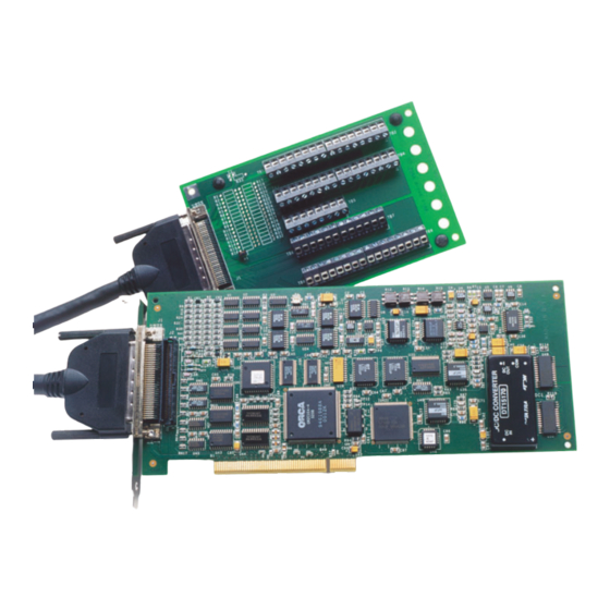
- Page 1 sales@artisantg.com artisantg.com (217) 352-9330 | Visit our website - Click HERE...
- Page 2 Title Page UM-16866-V DT3010 Series User’s Manual...
- Page 3 Other product and company names mentioned herein are trademarks or trade names of their respective companies. © 2010 Measurement Computing Corporation. All rights reserved. No part of this publication may be reproduced, stored in a retrieval system, or transmitted, in any form by any means, electronic, mechanical, by photocopying, recording, or otherwise without the prior written permission of Measurement Computing Corporation.
- Page 4 Page Radio and Television Interference This equipment has been tested and found to comply with CISPR EN55022 Class A and EN61000-6-1 requirements and also with the limits for a Class A digital device, pursuant to Part 15 of the FCC Rules. These limits are designed to provide reasonable protection against harmful interference when the equipment is operated in a commercial environment.
-
Page 6: Table Of Contents
Table of Contents Table of Contents About this Manual ........... . . 11 Intended Audience. - Page 7 Contents Configuring Resistors R17 to R32 - Current Shunt ......45 Configuring the STP268 Screw Terminal Panel ....... . 45 Configuring Jumper W1 - Common Ground Sense .
- Page 8 Contents Specifying a Single Channel ......... . . 105 Specifying One or More Channels .
- Page 9 Contents Digital I/O Features ............129 Digital I/O Lines .
- Page 10 Contents Using the DT3010 Calibration Utility ........163 Using the Auto-Calibration Procedure .
- Page 11 Contents Appendix C: Using Your Own Screw Terminal Panel ..... . . 213 Analog Inputs ............. . . 215 Single-Ended Inputs .
-
Page 12: About This Manual
About this Manual This manual describes how to set up and install the following components: • DT3010 Series software • DT3010 Series board • DT3010 Series Device Driver • DT740, STP268, or STP268-EC screw terminal panel It describes how to wire signals to the board and how to verify the board’s operation using the Quick DataAcq application. -
Page 13: Conventions Used In This Manual
About this Manual • Chapter “Wiring Signals,” describes how to wire signals to a DT3010 Series board using the DT740, STP268, or STP268-EC. • Chapter “Verifying the Operation of a DT3010 Series Board,” describes how to verify the operation of a DT3010 Series board with the Quick DataAcq application •... -
Page 14: Where To Get Help
About this Manual • DTx-EZ Getting Started Manual (UM-15428). This manual, available from Data Translation, describes how to use the ActiveX controls provided in DTx-EZ to access the capabilities of Data Translation data acquisition boards in Microsoft® Visual Basic or Visual C++. •... - Page 15 About this Manual...
-
Page 16: Chapter 1: Overview
Overview Features ..............Supported Software . -
Page 17: Features
Chapter 1 Features The DT3010 Series consists of the following high-speed, multifunction board types for the PCI bus: DT3010, DT3010-268, DT3010/32, DT3010/32-268, and DT3016. These board types differ in analog I/O resolution, output FIFO (first-in, first-out buffer) size, throughput, and connectors as shown in Table Table 1: Differences Among DT3010 Series Boards... - Page 18 Overview • Digital TTL triggering; one external hardware TTL input for the analog input subsystem and one external hardware TTL input for the analog output subsystem • Simultaneous analog input and analog output operations running at full speed • Software calibration of the analog input and output subsystems •...
-
Page 19: Supported Software
Chapter 1 Supported Software The following software is available for use with the DT3010 Series boards and on the Data Acquisition OMNI CD: • DT3010 Series Device Driver – The device driver is installed automatically when you install the software from the Data Acquisition OMNI CD. You need the device driver to use the DT3010 Series board with any of the supported software packages or utilities •... -
Page 20: Accessories
Overview Accessories The following optional accessories are available for DT3010 Series boards: • DT740 screw terminal panel – Screw terminal panel with two connectors to accommodate the analog I/O, digital I/O, and counter/timer signals provided by the DT3010, DT3010/32, and DT3016 boards. •... - Page 21 Chapter 1 − AC1315 – A 2-foot, 26-pin female to 26-pin female cable that connects a 7B Series backplane to the AC1393 cable. − AC1393 – A 6-inch, 26-pin male to 25-pin female adapter cable that connects a 7B Series backplane to the AC1315 cable; the AC1315 cable then connects to a STP268-EC screw terminal panel.
-
Page 22: Getting Started Procedure
Overview Getting Started Procedure The flow diagram shown in Figure 1 illustrates the steps needed to get started using a DT3010 Series board. This diagram is repeated in each getting started chapter; the shaded area in the diagram shows you where you are in the getting started procedure. Install the Board and Load the Device Driver (see Chapter 2... - Page 23 Chapter 1...
-
Page 24: Part 1: Getting Started
Part 1: Getting Started... -
Page 26: Chapter 2: Installing The Board And Loading The Device Driver
Installing the Board and Loading the Device Driver Unpacking ..............Unpacking . - Page 27 Chapter 2 Install the Board and Load the Device Driver (this chapter) Attach and Configure the Screw Terminal Panel (see Chapter 3 starting on page Wire Signals (see Chapter 4 starting on page Verify the Operation of the Board (see Chapter 5 starting on page...
-
Page 28: Unpacking
Installing the Board and Loading the Device Driver Unpacking Open the shipping box and remove the wrapped DT3010 Series board. CAUTION: Keep the board in its protective antistatic bag until you are ready to install it; this minimizes the likelihood of electrostatic damage. Verify that the following items are present: •... -
Page 29: Setting Up The Computer
Chapter 2 Setting up the Computer CAUTION: To prevent electrostatic damage that can occur when handling electronic equipment, use a ground strap or similar device when performing this installation procedure. To set up the computer, do the following: 1. Install the software from the Data Acquisition OMNI CD or Data Translation web site. Note: If you are using Windows 7, you must install the device driver before installing the board in the computer. -
Page 30: Setting Up Expansion Slots
Installing the Board and Loading the Device Driver Setting up Expansion Slots Once you have set up the computer, set up the expansion slots as follows: 1. Select a 32-bit or 64-bit PCI expansion slot. PCI slots are shorter than ISA or EISA slots and are usually white or ivory. Commonly, three PCI slots (one of which may be a shared ISA/PCI slot) are available. -
Page 31: Removing The Board For Handling
Chapter 2 Removing the Board for Handling To remove the board for handling, follow these steps: 1. Discharge any static electricity by holding the wrapped board in one hand while placing your other hand firmly on a metal portion of the computer chassis. 2. -
Page 32: Attaching The Ep324 Cable (Dt3010-268 Board Only)
Installing the Board and Loading the Device Driver Attaching the EP324 Cable (DT3010-268 Board Only) If you are using a DT3010-268 board and want to access the dynamic digital outputs, digital I/O port B, or counter/timers 2 and 3 of the board, you need to use the STP268 screw terminal panel and the EP324 cable that is shipped with the board. -
Page 33: Inserting The Dt3010 Series Board Into The Computer
Chapter 2 Inserting the DT3010 Series Board into the Computer Once you have set up the expansion slots and connected the EP324 cable to the board (if needed), do the following to insert the DT3010 Series board into the computer: 1. - Page 34 Installing the Board and Loading the Device Driver 3. When the bottom of the board contacts the bus connector, gently press down on the board until it clicks into place. CAUTION: Do not force the board into place. Moving the board from side to side during installation may damage the bus connector.
-
Page 35: Loading The Device Driver
Chapter 2 Loading the Device Driver To load the DT3010 Series device driver in: • Windows XP, follow the steps on page • Windows Vista, follow the steps on page • Windows 7, follow the steps on page Windows XP Once you have installed the DT3010 Series driver from the Data Acquisition OMNI CD, installed a DT3010 Series board, and powered up the host computer, the New Hardware Found dialog box appears. -
Page 36: Windows 7
Installing the Board and Loading the Device Driver 3. Click Install this driver software anyway. The driver files are installed. 4. Open the Control Panel. 5. Double-click the Open Layers Control Panel icon. 6. Select the DT3010 Series board to configure, and then click Advanced. By default, the prompt “Handles Overloaded Bus?”... - Page 37 Chapter 2...
-
Page 38: Chapter 3: Attaching And Configuring A Screw Terminal Panel
Attaching and Configuring a Screw Terminal Panel Attaching a Screw Terminal Panel ..........Configuring a Screw Terminal Panel. - Page 39 Chapter 3 Install the Board and Load the Device Driver (see Chapter 2 starting on page Attach and Configure the Screw Terminal Panel (this chapter) Wire Signals (see Chapter 4 starting on page Verify the Operation of the Board (see Chapter 5 starting on page...
-
Page 40: Attaching A Screw Terminal Panel
Attaching and Configuring a Screw Terminal Panel Attaching a Screw Terminal Panel If you are using the DT3010, DT3010/32, or DT3016 board, you first need to attach the DT740 screw terminal panel to the board before you can wire signals. If you are using the DT3010-268 or DT3010/32-268 board, you first need to attach the STP268 or STP268-EC screw terminal panel to the board before you can wire signals. -
Page 41: Attaching The Stp268-Ec Screw Terminal Panel
Chapter 3 The EP325 cable, which is provided as an option for the STP268 screw terminal panel, attaches the STP268 to either connector J1 or to the free end of cable EP324, which is attached to connector J2 (refer to Chapter 2 for more information on attaching the EP324 cable to connector J2). - Page 42 Attaching and Configuring a Screw Terminal Panel J1, 68-Pin Connector Jumpers J4, 26-Pin Connector J3, 26-Pin Connector J2, 50-Pin Connector Figure 7: STP268-EC Screw Terminal Panel Specific 5B and 7B Series backplanes that are supported include the following: − 5B01 – a16-channel backplane for 5B Series signal conditioning modules −...
-
Page 43: Attaching To The Dt3010-268 Or Dt3010/32-268 Board
Chapter 3 Attaching to the DT3010-268 or DT3010/32-268 Board The EP325 cable, which is available as an accessory to the STP268-EC screw terminal panel, attaches connector J1 on the STP268-EC to connector J1 on the DT3010-268 or DT3010/32-268 board. Figure 8 illustrates how to attach an STP268-EC screw terminal panel to the DT3010-268 or DT3010/32-268 board. -
Page 44: Attaching A 7B Series Backplane
Attaching and Configuring a Screw Terminal Panel Attaching a 7B Series Backplane To connect a 7B Series signal conditioning backplane to the STP268-EC screw terminal panel, refer to Figure 10 while completing the steps that follow: DT3010-268 or DT3010/32-268 Board J3 or J4 Connector J1 Connector AC1393... -
Page 45: Configuring A Screw Terminal Panel
Chapter 3 Configuring a Screw Terminal Panel This section describes how to locate and configure the jumpers and resistors on the DT740 or STP268 screw terminal panel for use with a DT3010 Series board. Configuring the DT740 Screw Terminal Panel Figure 12 shows the layout of the DT740 screw terminal panel, and shows the location of the jumper and resistors. -
Page 46: Configuring Resistors R1 To R16 - Bias Return
Attaching and Configuring a Screw Terminal Panel Configuring Resistors R1 to R16 - Bias Return Resistor locations R1 to R16 connect the low side of analog input channels to analog ground. These resistor locations are typically used when connecting differential inputs to analog input channels 0 to 15, where R1 corresponds to analog input channel 0, and R16 corresponds to analog input channel 15. -
Page 47: Configuring Jumper W1 - Common Ground Sense
Chapter 3 Jumper and Resistors Figure 13: Layout of the STP268 Screw Terminal Panel Configuring Jumper W1 - Common Ground Sense When shipped from the factory, jumper W1 connects the low side of the input amplifier (Amp Low) on the DT3010-268 or DT3010/32-268 board to analog ground. When using pseudo-differential analog inputs, remove jumper W1 and connect Amp Low to a remote common-mode voltage to reject offset voltages common to all 32 input channels. -
Page 48: Configuring Resistors R17 To R32 - Current Shunt
Attaching and Configuring a Screw Terminal Panel Configuring Resistors R17 to R32 - Current Shunt Resistor locations R17 to R32 are typically used to convert current to voltage on channels 0 to 15, where R17 corresponds to analog input channel 0, and R32 corresponds to analog input channel 15. - Page 49 Chapter 3...
-
Page 50: Chapter 4: Wiring Signals
Wiring Signals Preparing to Wire to a Screw Terminal Panel........Screw Terminal Assignments . -
Page 51: Panel
Chapter 4 Install the Board and Load the Device Driver (see Chapter 2 starting on page Attach and Configure the Screw Terminal Panel (see Chapter 3 starting on page Wire Signals (this chapter) Verify the Operation of the Board (see Chapter 5 starting on page... -
Page 52: Preparing To Wire To A Screw Terminal Panel
Wiring Signals Preparing to Wire to a Screw Terminal Panel This section describes wiring recommendations when connecting signals to a DT3010 board and screw terminal panel. Wiring Recommendations • Follow standard ESD procedures when wiring signals to the board. • Use individually shielded twisted-pair wire (size 14 to 26 AWG) when using a DT3010 Series board in highly noisy electrical environments. - Page 53 Chapter 4 • By default, the 5B01 and 7BP16-1 backplanes map to single-ended analog input channels 0 to 15. However, you can use channels 14 and 15 on the 5B01 or 7BP16-1 backplane as analog output channels 0 and 1 by configuring jumpers on the STP268-EC. Refer to Chapter 3 starting on page 37...
-
Page 54: Screw Terminal Assignments
Wiring Signals Screw Terminal Assignments This section describes the screw terminal assignments for the DT740, STP268, and STP268-EC screw terminal panels. DT740 Screw Terminal Assignments Screw terminals TB1 to TB56 on the DT740 screw terminal panel correspond to the analog I/O channels from the DT3010, DT3010/32, and DT3016 boards. - Page 55 Chapter 4 Table 2: Screw Terminal Assignments for Connector J1 on the DT740 Screw Terminal Panel J1 Pin Signal Description J1 Pin Signal Description Analog Input 00 Analog Input 08/00 Return Analog Input 01 Analog Input 09/01 Return Analog Input 02 Analog Input 10/02 Return Analog Input 03 Analog Input 11/03 Return...
- Page 56 Wiring Signals Table 3: Screw Terminal Assignments for Connector J2 on the DT740 Screw Terminal Panel J2 Pin Signal Description J2 Pin SIgnal Description 51, 52 Digital Ground User Clock Input 0 User Counter Output 0 External Gate 0 Digital Ground User Clock Input 1 User Counter Output 1 External Gate 1...
-
Page 57: Stp268 Screw Terminal Assignments
Chapter 4 STP268 Screw Terminal Assignments Screw terminals on the STP268 screw terminal panel are available for low-current signal conditioning applications. The supply on the DT3010-268 and DT3010/32-268 boards is current-limited through a 10 Ω resistor and is specified for a maximum load current of ±3 mA. The +5.0 V reference on the STP268 screw terminal panel is also current-limited through a 10 Ω... - Page 58 Wiring Signals Table 4: Screw Terminal Assignments for Connector J1 on the STP268 (cont.) Signal Description Signal Description Analog In 17 Analog In 25/ Analog Input 17 Return Analog In 18 Analog In 26/ Analog Input 18 Return Analog In 19 Analog In 27/ Analog Input 19 Return Analog In 20...
- Page 59 Chapter 4 Table 5: Screw Terminal Assignments for Connector J2 on the STP268 Signal Description Signal Description – Reserved – Reserved – Reserved – Reserved – Reserved – Reserved – Reserved – Reserved – Reserved – Reserved – Reserved – Reserved –...
-
Page 60: Stp268-Ec Screw Terminal Assignments
Wiring Signals Table 5: Screw Terminal Assignments for Connector J2 on the STP268 (cont.) Signal Description Signal Description 4, 35, Digital Ground User Clock Input 3 User Counter Output 3 External Gate 3 Digital I/O Bank B0 Digital I/O Bank B1 Digital I/O Bank B2 Digital I/O Bank B3 Digital I/O Bank B4... - Page 61 Chapter 4 Table 6: Screw Terminal Assignments for Connector J1 on the STP268-EC (cont.) Signal Description Signal Description Analog Input 03 Analog Input 02 Analog Input 01 Analog Input 00 Digital Ground External Gate 1 External Gate 0 User Clock Input 1 Digital Ground Digital I/O Bank A7 Digital I/O Bank A6...
- Page 62 Wiring Signals Table 7 lists the screw terminal assignments for connector J2 on the STP268-EC screw terminal panel. Table 7: Screw Terminal Assignments for Connector J2 on the STP268-EC J2 Pin Signal Description J2 Pin Signal Description Digital I/O 3 Digital I/O 2 Digital I/O 1 Digital I/O 0...
- Page 63 Chapter 4 Table 9 lists the screw terminal assignments for connector J4 on the STP268-EC screw terminal panel. Table 9: Screw Terminal Assignments for Connector J4 on the STP268-EC J4 Pin SIgnal Description J4 Pin SIgnal Description Analog Input 23 Analog Input 22 Analog Input 21 Analog Input 20...
-
Page 64: Connecting Analog Input Signals
Wiring Signals Connecting Analog Input Signals The DT740, STP268, and STP268-EC screw terminal panels support both voltage and current loop inputs. You can connect analog input voltage signals to the screw terminal panels in the following configurations: • Single-ended – Choose this configuration when you want to measure high-level signals, noise is not significant, the source of the input is close to the screw terminal panel, and all the input signals are referred to the same common ground. - Page 65 Chapter 4 Jumper W1 DT740 or STP268 Panel Installed Signal Source (Amp Low) − TB33 Vsource TB34 Analog In 0 − Analog In 1 Vsource Analog Ground Note that the signals shown for the STP268 screw terminal panel correspond to connector J1. Figure 14: Connecting Single-Ended Voltage Inputs to the DT740 or STP268 (Shown for Channels 0 and 1) Figure 15...
-
Page 66: Connecting Pseudo-Differential Voltage Inputs
Wiring Signals Connecting Pseudo-Differential Voltage Inputs Figure 16 shows how to connect pseudo-differential voltage inputs to the DT740 or STP268 screw terminal panel. DT740 or STP268 Panel Signal Source − TB33 Vsource Analog In 0 TB34 Analog In 1 − Vsource Remove Jumper W1 to use Amp Low as a remote ground sense. -
Page 67: Connecting Differential Voltage Inputs
Chapter 4 STP268-EC Panel Signal Source − TB18 Vsource Analog In 0 TB34 TB33 − Vsource Analog In 1 TB52 Amp Low Analog Ground *Make this connection as close to V sources possible to reduce ground loop errors. is the common-mode voltage for all 32 analog inputs. - Page 68 Wiring Signals Analog In 0 TB34 DT740 Floating STP268 Signal Panel Analog In 0 Source Return − You can use resistor R1 to connect the low side of Analog Ground channel 0 to analog ground. Bridge Analog In 0 TB34 DT740 STP268 Analog In 0...
- Page 69 Chapter 4 STP268-EC Panel TB68 TB34 Analog In 0 Floating Signal Source Analog In 0 TB52 Return − User- Supplied Resistor Analog Ground Supply a bias return resistor to connect the low side of channel 0 to analog ground. Bridge TB68 TB34 Analog In 0...
- Page 70 Wiring Signals DT740 or STP268 Panel Analog In 0 TB34 Grounded Signal Analog In 0 Source Return − Signal Source Ground V Analog Ground Resistor R1 should be installed for bias return in case the external ground is floating. Note that the signals shown for the STP268 screw terminal panel correspond to connector Figure 20: Connecting Differential Voltage Inputs from a Grounded Signal Source to the DT740 or STP268 (Shown for Channel 0)
-
Page 71: Connecting Current Loop Inputs
Chapter 4 Connecting Current Loop Inputs Figure 22 shows how to connect a current loop input to the DT740 screw terminal panel, Figure 23 shows how to connect a current loop input to the STP268 screw terminal panel, and Figure 24 shows how to connect a current loop input to the STP268-EC screw terminal panel. - Page 72 Wiring Signals User-Supplied STP268-EC Panel Shunt Resistor 4 to 20 mA TB68 TB34 Analog Input 0 User-Supplied Bias Return Resistor Analog Input 0 Return Analog Ground TB52 Supply a current shunt resistor to convert current to voltage; Ω for 4 to 20 mA = 1 to 5 V. The common side of the external loop supply must either connect to analog ground or, if needed, to a bias return resistor.
-
Page 73: Connecting Analog Output Signals
Chapter 4 Connecting Analog Output Signals Figure 25 shows how to connect analog output voltage signals to the DT740 screw terminal panel, Figure 26 shows how to connect analog output voltage signals to the STP268 screw terminal panel, and Figure 27 shows how to connect analog output voltage signals to the STP268-EC screw terminal panel. - Page 74 Wiring Signals STP268-EC Panel TB17 Analog Output 0 Load TB51 Analog Ground Figure 27: Connecting Analog Output Voltages to the STP268-EC (Shown for Channel 0)
-
Page 75: Connecting Digital I/O Signals
Chapter 4 Connecting Digital I/O Signals Figure 28 shows how to connect digital input signals to the DT740 screw terminal panel, Figure 29 shows how to connect digital input signals to the STP268 screw terminal panel, and Figure 30 shows how to connect digital input signals to the STP268-EC screw terminal panel. DT740 Panel Digital I/O Bank A 0 TB89... - Page 76 Wiring Signals STP268-EC Panel Digital Ground Digital I/O Bank A 1 TTL Inputs Digital I/O Bank A 0 Figure 30: Connecting Digital Inputs to the STP268-EC (Shown for Lines 0 and 1, Bank A) Figure 31 shows how to connect a digital output signal to the DT740 screw terminal panel, Figure 32 shows how to connect a digital output signal to the STP268 screw terminal panel, Figure 33...
- Page 77 Chapter 4 0 Out = LED On STP268 Panel TB61 Ω Digital I/O Bank B 0 TB51 Digital Ground Note that the signals shown for the STP268 screw terminal panel correspond to connector J2. Figure 32: Connecting Digital Outputs to the STP268 (Shown for Line 0, Bank B) STP268-EC Panel Digital Ground 0 Out = LED On...
-
Page 78: Connecting Counter/Timer Signals
Wiring Signals Connecting Counter/Timer Signals The DT3010 Series boards with the DT740, STP268, or STP268-EC screw terminal panel provide counter/timers that you can use for the following operations: • Event counting • Frequency measurement • Pulse output (rate generation, one-shot, and repetitive one-shot) This section describes how to connect counter/timer signals to perform these operations. - Page 79 Chapter 4 User Clock Input 0 TB58 TB60 Signal Source TB61 TB83 Digital Ground DT740 Panel TB108 Digital Shield In this example, a software gate is used to start the event counting operation. Figure 35: Connecting Event Counting Applications to the DT740 (Shown for Clock Input 0 without an External Gate)
- Page 80 Wiring Signals User User Clock Input 0 Counter TB58 Output 0 TB59 Gate 0 TB60 Signal Source TB61 TB62 User Clock Digital Ground Gate 1 TB83 Input 1 TB64 External Gating DT740 Panel Switch Digital Ground TB108 Digital Shield Note that you can also internally cascade counters using software;...
- Page 81 Chapter 4 STP268 Panel User Clock Input 0 TB54 TB56 Signal Source TB57 Digital Ground External Gating Gate 0 Switch Digital Ground Note that the signals shown for the STP268 screw terminal panel correspond to connector J1. In this example, rising clock edges are counted while the gate is active.
- Page 82 Wiring Signals STP268 Panel User User Clock Input 0 Counter TB54 Output 0 TB55 Signal Source TB56 Gate 0 TB57 TB58 User Clock Gate 1 Input 1 TB60 External Gating Switch Digital Ground Note that the signals shown for the STP268 screw terminal panel correspond to connector J1.
- Page 83 Chapter 4 STP268-EC Panel TB35 TB37 Digital Ground Signal Source User Clock Input 0 External Gating Switch Digital Ground Gate 0 In this example, rising clock edges are counted while the gate is active. Figure 40: Connecting Event Counting Applications to the STP268-EC (Shown for Clock Input 0 and External Gate 0) STP268-EC Panel Digital Ground...
-
Page 84: Connecting Frequency Measurement Signals
Wiring Signals STP268-EC Panel TB35 Gate 1 Digital Ground TB36 TB37 Signal TB38 Source User User Clock Clock User Clock Input 0 Output 0 Input 1 External Gating Switch Digital Ground Gate 0 Note that you can internally cascade counters using software; if you internally cascade the counters, you do not have to make the external cascading connections. - Page 85 Chapter 4 DT740 Panel User Clock Input 0 TB58 Gate 0 TB60 Signal Source TB61 User TB63 Digital Ground Counter TB83 Output 1 TB108 Digital Shield Figure 43: Connecting Frequency Measurement Applications to the DT740 Screw Terminal Panel (Shown for Clock Input 0 and External Gate 0) STP268 Panel User Clock Input 0 TB54...
-
Page 86: Connecting Pulse Output Signals
Wiring Signals STP268-EC Panel User Clock Output 1 Digital Ground TB37 Signal Gate 0 Source User Clock Input 0 Figure 45: Connecting Frequency Measurement Applications to the STP268-EC Screw Terminal Panel (Shown for Clock Input 0 and External Gate 0) Connecting Pulse Output Signals Figure Figure... - Page 87 Chapter 4 User Digital Ground TB57 Counter TB58 Output 0 User Clock Input 0 TB59 TB60 Signal Source TB61 TB62 User Clock Input 1 External DT740 Panel Gating Switch Gate 0 Digital Ground TB108 Digital Shield Note that you can also internally cascade counters using software;...
- Page 88 Wiring Signals Figure Figure 50, and Figure 51 show examples of connecting pulse output applications to the STP268 screw terminal panel. Other combinations of signals can be used. STP268 Panel User Counter Output 0 TB55 TB56 Heater TB57 Controller Digital Ground External Gating Gate 0...
- Page 89 Chapter 4 STP268 Panel User Digital Ground TB53 Counter TB54 Output 0 User Clock Input 0 TB55 Signal Source TB57 TB58 User Clock Input 1 TB60 Digital Ground One-Shot Trigger Gate 1 Note that the signals shown for the STP268 screw terminal panel correspond to connector J1.
- Page 90 Wiring Signals STP268-EC Panel TB35 Digital Ground TB37 Signal TB38 Source User User Clock Clock User Clock Input 0 Output 0 Input 1 External Gating Switch Digital Ground Gate 0 Figure 53: Cascading Counters to the STP268-EC (Shown for Rate Generation Using Counters 0 and 1 and External Gate 0) STP268-EC Panel TB35 Digital Ground...
- Page 91 Chapter 4...
-
Page 92: Chapter 5: Verifying The Operation Of A Dt3010 Series Board
Verifying the Operation of a DT3010 Series Board Running the Quick DataAcq Application......... Testing Single-Value Analog Input . - Page 93 Chapter 5 Install the Board and Load the Device Driver (see Chapter 2 starting on page Attach and Configure the Screw Terminal Panel (see Chapter 3 starting on page Wire Signals (see Chapter 4 starting on page Verify the Operation of the Board (this chapter) You can verify the operation of a DT3010 Series board using the Quick DataAcq application.
-
Page 94: Running The Quick Dataacq Application
Verifying the Operation of a DT3010 Series Board Running the Quick DataAcq Application The Quick DataAcq application is installed automatically when you install the driver software. To run the Quick DataAcq application, do the following: 1. If you have not already done so, power up your computer and any attached peripherals. 2. -
Page 95: Testing Single-Value Analog Input
Chapter 5 Testing Single-Value Analog Input To verify that the board can read a single analog input value, do the following: 1. Connect a voltage source, such as a function generator, to analog input channel 0 (differential mode) on the DT3010 Series board. Refer to page 66 for an example of how to connect a differential analog input. -
Page 96: Testing Single-Value Analog Output
Verifying the Operation of a DT3010 Series Board Testing Single-Value Analog Output To verify that the board can output a single analog output value, do the following: 1. Connect an oscilloscope or voltmeter to DAC0 on the board. Refer to page 72 for an example of how to connect analog output signals. -
Page 97: Testing Continuous Analog Input
Chapter 5 Testing Continuous Analog Input To verify that the board can perform a continuous analog input operation, do the following: 1. Connect known voltage sources, such as the outputs of a function generator, to analog input channels 0 and 1 on the DT3010 Series board (using the differential configuration). Refer to page 66 for an example of how to connect a differential analog input. -
Page 98: Testing Single-Value Digital Input
Verifying the Operation of a DT3010 Series Board Testing Single-Value Digital Input To verify that the board can read a single digital input value, do the following: 1. Connect a digital input to digital input line 0 of port A on the DT3010 Series board. Refer page 74 for an example of how to connect a digital input. -
Page 99: Testing Single-Value Digital Output
Chapter 5 Testing Single-Value Digital Output To verify that the board can output a single digital output value, do the following: 1. Connect a digital output to digital output line 0 of port B on the DT3010 Series board. Refer to page 74 for an example of how to connect a digital output. -
Page 100: Testing Frequency Measurement
Verifying the Operation of a DT3010 Series Board Testing Frequency Measurement To verify that the board can perform a frequency measurement operation, do the following: 1. Wire an external clock source to counter/timer 0 on the DT3010 Series board. Refer to page 83 for an example of how to connect a an external clock for a frequency measurement operation. -
Page 101: Testing Pulse Output
Chapter 5 Testing Pulse Output To verify that the board can perform a pulse output operation, do the following: 1. Connect a scope to counter/timer 0 on the DT3010 Series board. Refer to page 85 for an example of how to connect a scope (a pulse output) to counter/timer 0. Note: The Quick DataAcq application works only with counter/timer 0. -
Page 102: Part 2: Using Your Board
Part 2: Using Your Board... -
Page 104: Chapter 6: Principles Of Operation
Principles of Operation Analog Input Features ............Analog Output Features . - Page 105 Chapter 6 This chapter describes the analog input, analog output, digital I/O, counter/timer, and synchronous features of the DT3010 Series boards. To frame the discussions, refer to the block diagram shown in Figure 55. Note that bold entries indicate signals you can access. A/D Trig A/D Trig Out Trigger/Clock...
-
Page 106: Analog Input Features
Principles of Operation Analog Input Features This section describes the features of the analog input (A/D) subsystem, including the following: • Analog input resolution • Analog input channels • Input ranges and gains • A/D sample clock sources • Analog input conversion modes •... -
Page 107: Specifying One Or More Channels
Chapter 6 Specifying One or More Channels DT3010 Series boards can read data from one or more analog input channels using an analog input channel list. You can group the channels in the list sequentially (either starting with 0 or with any other analog input channel), or randomly. -
Page 108: Input Ranges And Gains
Principles of Operation Two dynamic digital output lines are provided: 0 and 1. These lines are set to a value of 0 on power up; a reset does not affect the values of the dynamic digital output lines. Note that these lines are provided in addition to the other 16 digital I/O lines;... -
Page 109: A/D Sample Clock Sources
Chapter 6 Through software, specify the range as 0 to 10 V for unipolar signals or − 10 V to +10 V for bipolar signals. Note that the range applies to the entire analog input subsystem, not to a specific channel. DT3010 Series boards also provide gains 1, 2, 4, and 8, which are programmable per channel. -
Page 110: Internal A/D Sample Clock
Principles of Operation Note: If you enter digital I/O channel 32 in the channel list, the A/D sample clock (internal or external) also paces the acquisition of the 16 digital input lines. The following subsections describe the internal and external A/D sample clocks in more detail. -
Page 111: Analog Input Conversion Modes
Chapter 6 Note: The DT3010-268 board only provides an External A/D Trigger and Clock Enable signal. This signal is pulled high on the DT3010-268 board by a 22 kΩ resistor. You can use this signal to enable or disable the external digital trigger and the external A/D sample clock. A high signal enables both the external digital trigger and the external A/D sample clock, while a low signal disables both the external digital trigger and the external A/D sample clock. -
Page 112: Triggered Scan Mode
Principles of Operation To select continuously-paced scan mode, use software to specify the dataflow as Continuous, ContinuousPreTrigger, or Continuous PrePostTrigger; refer to page 115 for more information about these trigger acquisition modes. The initial trigger source depends on the trigger acquisition mode selected; refer to page 113 for more information on the supported trigger acquisition modes and trigger sources. -
Page 113: Externally-Retriggered Scan Mode
Chapter 6 For example, if you are using 512 channels in the channel list, scanning the channel list 256 times every trigger or retrigger, and using an A/D sample clock with a frequency of 1 MHz, set the maximum retrigger frequency to 7.62 Hz, since 7.62 Hz = ( 512 * 256) +2 μs 1 MHz... -
Page 114: Triggers
Principles of Operation The conversion rate of each channel is determined by the frequency of the A/D sample clock; refer to page 108 for more information on the A/D sample clock. The conversion rate of each scan is determined by the period between external retriggers; therefore, it cannot be accurately controlled. -
Page 115: External Digital (Ttl) Trigger
Chapter 6 External Digital (TTL) Trigger For analog input operations, an external digital trigger event occurs when the DT3010 Series board detects either a rising or falling edge on the External A/D TTL Trigger input signal connected to screw terminal 77 on the DT740 screw terminal panel, screw terminal 49 on the STP268 screw terminal panel (attached to connector J1), or screw terminal 14 on the STP268-EC screw terminal panel. -
Page 116: Trigger Acquisition Modes
Principles of Operation Note: If you are using an analog threshold trigger to trigger both the A/D and the D/A subsystems, ensure that you use the same analog trigger type for both subsystems (either external or one of the analog input channels). The polarity of the triggers, however, can be different. -
Page 117: Pre-Trigger Acquisition
Chapter 6 Figure 58 illustrates the same example using triggered scan mode (either a software or external retrigger source). The multiscan count is 2 indicating that the channel list will be scanned twice per trigger or retrigger. In this example, post-trigger analog input data is acquired on each clock pulse of the A/D sample clock until the channel list has been scanned twice;... - Page 118 Principles of Operation If you are using software-retriggered scan mode and the post-trigger event has not occurred, the board continues to acquire pre-trigger data using the Triggered Scan Counter to clock the operation. When the post-trigger event occurs, the operation stops. Refer to page 111 for more information on software-retriggered scan mode.
-
Page 119: About-Trigger Acquisition
Chapter 6 About-Trigger Acquisition Use about-trigger acquisition mode when you want to acquire data both before and after a specific external event occurs. This operation is equivalent to doing both a pre-trigger and a post-trigger acquisition. Using software, specify the following parameters: •... -
Page 120: Data Format And Transfer
Principles of Operation Chan 0 Chan 0 Chan 0 Chan 0 Chan 0 Chan 0 Chan 1 Chan 1 Chan 1 Chan 1 Chan 1 Chan 1 . . . Sample Clock Pre-trigger data acquired Post-trigger data acquired Pre-trigger event occurs Post-trigger event occurs Figure 61: Continuous About-Trigger Mode Figure 62... -
Page 121: Error Conditions
Chapter 6 The board packs two input samples (an even and an odd sample) into each transfer to the host computer. Samples corresponding to entries 0, 2, 4, and so on, in the channel list are considered even samples; samples corresponding to entries 1, 3, 5, and so on, in the channel list are considered odd samples. - Page 122 Principles of Operation If any of these error conditions occurs, the board stops acquiring and transferring data to the host computer. Note: DT-Open Layers reports any of these errors as an overrun message.
-
Page 123: Analog Output Features
Chapter 6 Analog Output Features Two analog output (D/A) subsystems are provided on DT3010 Series boards. The first D/A subsystem contains the majority of analog output features. The second is dedicated to threshold triggering only (refer to page 125 for more information on analog threshold triggering). -
Page 124: Specifying One Or More Channels
Principles of Operation Specifying One or More Channels You can specify one or two analog output channels in the analog output channel list, either starting with DAC 0 or with DAC 1. Values are output simultaneously to the entries in the channel list. Output Ranges and Gains Each DAC on the DT3010 Series board can output bipolar analog output signals in the range of ±10 V. -
Page 125: External D/A Output Clock
Chapter 6 External D/A Output Clock The external D/A output clock is useful when you want to pace analog output operations at rates not available with the internal D/A output clock, if you want to pace at uneven intervals, or if you want to start pacing when an external event occurs. Connect an external D/A output clock to screw terminal 74 on the DT740 screw terminal panel, screw terminal 46 on the STP268 screw terminal panel (attached to connector J1), or screw terminal 44 on the STP268-EC screw terminal panel. -
Page 126: Analog Threshold Trigger
Principles of Operation Analog Threshold Trigger For analog output operations, an analog trigger event occurs when the DT3010 Series board detects a transition from above a threshold level to below a threshold level (falling edge), or a transition from below a threshold level to above a threshold level (rising edge). The following analog threshold trigger sources are available: •... -
Page 127: Continuously-Paced Analog Output
Chapter 6 To stop a continuously-paced analog output operation, you can stop sending data to the board, letting the board stop when it runs out of data, or you can perform either an orderly stop or an abrupt stop using software. In an orderly stop, the board finishes outputting the specified number of samples, then stops;... -
Page 128: Waveform Generation
Principles of Operation Waveform Generation Use waveform generation mode if you want to output waveforms repetitively. Before this process can begin, the host computer must transfer the entire waveform pattern to output to the DACs from a single buffer allocated in computer memory into the output FIFO on the board. -
Page 129: Error Conditions
Chapter 6 The host computer must pack two output samples (an even and an odd sample) into each transfer to the DT3010 Series board. The even sample is written to the output FIFO first, followed by the odd sample. If the analog output channel list contains two DACs, the even samples (0, 2, 4, and so on) are written to channel entry 0 in the analog output channel list;... -
Page 130: Digital I/O Features
Principles of Operation Digital I/O Features This section describes the following features of the digital I/O subsystem: • Digital I/O lines • Digital I/O resolution • Digital I/O operation modes Digital I/O Lines DT3010 Series boards support 16 digital I/O lines through the digital input (DIN) and output (DOUT) subsystems;... - Page 131 Chapter 6 • Continuous digital input takes full advantage of the capabilities of the DT3010 Series boards. In this mode, you enter all 16 digital input lines as channel 32 of the analog input channel list using software. This mode is programmed through the A/D subsystem. Using this mode, you can specify a clock source, scan mode, trigger source, trigger acquisition mode, and buffer for the digital input operation.
-
Page 132: Counter/Timer Features
Principles of Operation Counter/Timer Features The counter/timer circuitry on the board provides the clocking circuitry used by the A/D and D/A subsystems as well as several user counter/timer features. This section describes the following user counter/timer features: • Units • C/T clock sources •... -
Page 133: Internal C/T Clock
Chapter 6 Internal C/T Clock The internal C/T clock uses a 20 MHz time base. Counter/timer operations start on the rising edge of the clock input signal. Through software, specify the clock source as internal and the frequency at which to pace the counter/timer operation (this is the frequency of the clock output signal). -
Page 134: Gate Types
Principles of Operation Specify internal cascade mode in software. The rising edge of the clock input signal is active. Through software, specify the clock source as internal and the frequency at which to pace the counter/timer operation (this is the frequency of the clock output signal). The maximum frequency that you can specify for the clock output signal is 10 MHz. -
Page 135: Pulse Output Types And Duty Cycles
Chapter 6 Table 12: Gate Input Signals Screw Terminal on Screw Terminal on Screw Terminal Counter/Timer the DT740 the STP268 on STP268-EC TB60 TB56 TB37 TB64 TB60 TB36 TB68 TB56 – TB72 TB60 – a. STP268 must be attached to connector J1. b. -
Page 136: Counter/Timer Operation Modes
Principles of Operation Figure 64 illustrates a low-to-high pulse with a duty cycle of approximately 30%. Active Pulse Width high pulse low pulse Total Pulse Period Figure 64: Example of a Low-to-High Pulse Output Type Counter/Timer Operation Modes DT3010 Series boards support the following counter/timer operation modes: •... - Page 137 Chapter 6 DT740 Screw Terminal Panel User Clock Input 0 TB58 TB60 Signal Source TB61 TB83 Digital Ground External Gating Switch Gate 0 Digital Ground TB108 Digital Shield Figure 65: Connecting Event Counting Signals (Shown for Clock Input 0 and External Gate 0) Figure 66 shows an example of an event counting operation.
-
Page 138: Frequency Measurement
Principles of Operation Frequency Measurement Use frequency measurement mode to measure the frequency of the signal from counter’s associated clock input source over a specified duration. In this mode, use an external C/T clock source; refer to page 131 for more information on the external C/T clock source. One way to perform a frequency measurement is to use the same wiring as an event counting application that does not use an external gate signal, as shown in Figure... - Page 139 Chapter 6 DT740 Screw Terminal Panel User Clock Input 0 TB58 Gate 0 TB60 Signal Source TB61 User TB63 Digital Ground Counter TB83 Output 1 Figure 68: Connecting Frequency Measurement Signals (Shown for Clock Input 0 and External Gate 0) In this configuration, use software to set up the counter/timers as follows: 1.
-
Page 140: Rate Generation
Principles of Operation 3 Events Counted External C/T Clock Input Signal Duration over which the frequency is measured = 300 ms frequency frequency measurement measurement stops starts Figure 69: Example of Frequency Measurement Rate Generation Use rate generation mode to generate a continuous pulse output signal from the counter; this mode is sometimes referred to as continuous pulse output or pulse train output. - Page 141 Chapter 6 DT740 Screw Terminal Panel User Counter Input 0 User Counter Output 0 TB59 Heater TB61 Controller Digital Ground TB83 Signal Source Digital Ground Figure 70: Connecting Rate Generation Signals (Shown for Counter Output 0; a Software Gate is Used) Figure 71 shows an example of an enabled rate generation operation using an external C/T clock source with an input frequency of 4 kHz, a clock divider of 4, a low-to-high pulse type,...
-
Page 142: One-Shot
Principles of Operation Continuous Pulse Output Operation Starts External C/T Clock Input Signal (4 kHz) Pulse Output 25% duty cycle Signal Figure 72: Example of Rate Generation Mode with a 25% Duty Cycle One-Shot Use one-shot mode to generate a single pulse output signal from the counter when the operation is triggered (determined by the gate input signal). - Page 143 Chapter 6 DT740 Screw Terminal Panel User Counter Output 0 TB59 TB60 Heater TB61 Controller Digital Ground TB83 External Gating Switch Gate 0 Digital Ground Figure 73: Connecting One-Shot Signals (Shown for Counter Output 0 and Gate 0) Figure 74 shows an example of a one-shot operation using an external gate input (rising edge), a clock output frequency of 1 kHz (pulse period of 1 ms), and a low-to-high pulse type.
-
Page 144: Repetitive One-Shot
Principles of Operation Repetitive One-Shot Use repetitive one-shot mode to generate a pulse output signal each time the board detects a trigger (determined by the gate input signal). You can use this mode to clean up a poor clock input signal by changing its pulse width, then outputting it. In repetitive one-shot mode, the internal C/T clock source is more useful than an external C/T clock source;... -
Page 145: Synchronizing A/D And D/A Subsystems
Chapter 6 Synchronizing A/D and D/A Subsystems You can synchronize the operation of the A/D and D/A subsystems providing that they are not performing single-value operations. Refer to page 110 page 125 for more information on single-value operations. You can synchronize the A/D and D/A subsystems in two ways: by synchronizing the triggers and by synchronizing the clocks. -
Page 146: Synchronizing The Clocks
Principles of Operation Synchronizing the Clocks You can synchronize the clocks of the A/D and D/A subsystems as follows: • Internal Sample Clocks – Using software, specify the clock source as the internal A/D sample clock for the A/D subsystem and the internal D/A output clock for the D/A subsystem. - Page 147 Chapter 6...
-
Page 148: Chapter 7: Supported Device Driver Capabilities
Supported Device Driver Capabilities Data Flow and Operation Options..........Buffering . - Page 149 Chapter 7 The DT3010 Series Device Driver provides support for the analog input (A/D), analog output (D/A), digital input (DIN), digital output (DOUT), and counter/timer (C/T) subsystems. For information on how to configure the device driver, refer to page Table 14: DT3010 Series Subsystems DT3010 Series DOUT QUAD...
-
Page 150: Data Flow And Operation Options
Supported Device Driver Capabilities Data Flow and Operation Options Table 15: DT3010 Series Data Flow and Operation Options DT3010 Series DOUT QUAD Single-Value Operation Support SupportsSingleValue Simultaneous Single-Value Output Operations SupportsSetSingleValues Continuous Operation Support SupportsContinuous Continuous Operation until Trigger SupportsContinuousPreTrigger Continuous Operation before &... -
Page 151: Buffering
Chapter 7 Buffering Table 16: DT3010 Series Buffering Options DT3010 Series DOUT QUAD Buffer Support SupportsBuffering Single Buffer Wrap Mode Support SupportsWrapSingle Inprocess Buffer Flush Support SupportsInProcessFlush a. The data from the DT3010 board is transferred to the host in 64 byte segments; therefore, the number of valid samples that can be moved is always a multiple of 64. -
Page 152: Data Encoding
Supported Device Driver Capabilities Data Encoding Table 18: DT3010 Series Data Encoding Options DT3010 Series DOUT QUAD Binary Encoding Support SupportsBinaryEncoding Twos Complement Support SupportsTwosCompEncoding Returns Floating-Point Values ReturnsFloats Channels Table 19: DT3010 Series Channel Options DT3010 Series DOUT QUAD Number of Channels NumberOfChannels SE Support... -
Page 153: Gain
Chapter 7 Gain Table 20: DT3010 Series Gain Options DT3010 Series DOUT QUAD Programmable Gain Support SupportsProgrammableGain Number of Gains NumberOfSupportedGains Gains Available SupportedGains 1, 2, 4, 8 1 Ranges Table 21: DT3010 Series Range Options DT3010 Series DOUT QUAD Number of Voltage Ranges NumberOfRanges Available Ranges... -
Page 154: Thermocouple And Rtd Support
Supported Device Driver Capabilities Thermocouple and RTD Support Table 23: DT3010 Series Thermocouple and RTD Support Options DT3010 Series DIN DOUT C/T QUAD Thermocouple Support SupportsThernocouple RTD Support SupportsRTD Resistance Support ReturnsOhms Voltage Converted to Temperature in Hardware SupportsTemperatureDataInStream Supported Thermocouple Types ThermocoupleType Supported RTD Types RTDType... -
Page 155: Triggers
Chapter 7 Triggers Table 25: DT3010 Series Trigger Options DT3010 Series DOUT QUAD Software Trigger Support SupportsSoftwareTrigger External Positive TTL Trigger Support SupportsPosExternalTTLTrigger External Negative TTL Trigger Support SupportsNegExternalTTLTrigger External Positive TTL Trigger Support for Single-Value Operations SupportsSvPosExternalTTLTrigger External Negative TTL Trigger Support for Single-Value Operations SupportsSvNegExternalTTLTrigger Positive Threshold Trigger Support... -
Page 156: Clocks
Supported Device Driver Capabilities Clocks Table 26: DT3010 Series Clock Options DT3010 Series DOUT QUAD Internal Clock Support SupportsInternalClock External Clock Support SupportsExternalClock Simultaneous Input/Output on a Single Clock Signal SupportsSimultaneousClocking Base Clock Frequency BaseClockFrequency 20 MHz 20 MHz 20 MHz Maximum Clock Divider MaxExtClockDivider 65536... -
Page 157: Counter/Timers
Chapter 7 Counter/Timers Table 27: DT3010 Series Counter/Timer Options DT3010 Series DOUT QUAD Cascading Support SupportsCascading Event Count Mode Support SupportsCount Generate Rate Mode Support SupportsRateGenerate One-Shot Mode Support SupportsOneShot Repetitive One-Shot Mode Support SupportsOneShotRepeat Up/Down Counting Mode Support SupportsUpDown Edge-to-Edge Measurement Mode Support SupportsMeasure Continuous Edge-to-Edge Measurement... - Page 158 Supported Device Driver Capabilities Table 27: DT3010 Series Counter/Timer Options (cont.) DT3010 Series DOUT QUAD Gate-Rising Edge Type SupportsGateRising Interrupt-Driven Operations SupportsInterrupt a. For one-shot and repetitive one-shot operations, the pulse width is set automatically to 100%. b. High-edge and low-edge are supported for one-shot and repetitive one-shot modes. High-level and low-level are supported for event counting and rate generation modes.
- Page 159 Chapter 7...
-
Page 160: Chapter 8: Calibration
Calibration Calibrating the Analog Input Subsystem ........Calibrating the Analog Output Subsystem . - Page 161 Chapter 8 The DT3010 Series boards are calibrated at the factory and should not require calibration for initial use. We recommend that you check and, if necessary, readjust the calibration of the analog input and analog output circuitry on the DT3010 Series boards every six months. The DT3010 Calibration Utility is provided for calibrating the DT3010, DT3010-268, DT3010/32, and DT3010/32-268 boards.
-
Page 162: Calibrating The Analog Input Subsystem
Calibration Calibrating the Analog Input Subsystem This section describes how to configure the DT740, STP268, or STP268-EC screw terminal panel for an internal or external reference, and how to use the DT3010 and DT3016 calibration utilities to calibrate the analog input subsystem of the board. Choosing a Calibration Reference To calibrate the analog input circuitry, you can use either of the following references: •... -
Page 163: Configuring For An External Reference
Chapter 8 3. Connect Analog In 1 to Analog In 1 Return and Analog Ground. DT740 Screw STP268 Screw STP268-EC Signal Terminal Terminal on J1 Screw Terminal Analog Input 1 TB33 Analog Input 1 Return TB67 Analog Ground TB34 TB34 TB52 For the DT3010, DT3010-268, DT3010/32, or DT3010/32-268 board, follow the instructions on page... -
Page 164: Using The Dt3010 Calibration Utility
Calibration 4. Connect Analog In 1 and Analog In 1 Return to Analog Ground. DT740 Screw STP268 Screw STP268-EC Signal Terminal Terminal on J1 Screw Terminal Analog Input 1 TB33 Analog Input 1 Return TB67 Analog Ground TB34 TB34 TB52 For the DT3010, DT3010-268, DT3010/32, or DT3010/32-268 board, follow the instructions on page 163. -
Page 165: Using The Manual Calibration Procedure
Chapter 8 2. Select the name of the DT3010, DT3010-268, DT3010/32, or DT3010/32-268 board to configure from the combo box, and then click OK. 3. From the main menu of the DT3010 Calibration Utility, click Calibrate, and then A/D. 4. In the Reference Source box, select the reference that you are using (Internal or External; Internal is the default). -
Page 166: Calibrating The Pgh Zero Setting
Calibration 11. Click the increment or decrement arrows in the Manual Adjustment box until the display reads just above 0 V, then use the decrement arrow until the first value of 0 V is displayed (within 0.0024 V). 12. In the Range box, select Unipolar, and then +FS (for full-scale). 13. -
Page 167: Using The Dt3016 Calibration Utility
Chapter 8 Note: If you have a version of the board without the -PBF (lead-free) designator, this potentiometer is labelled R4. 3. Click Quit when you are finished. Once you have finished this procedure, continue with “Calibrating the Analog Output Subsystem”... - Page 168 Calibration 5. In the Auto Calibration box, click Go. The bipolar (zero and full-scale) and unipolar (zero and full-scale) ranges are automatically calibrated, and the calibration values are displayed. The bipolar readings should be within 0.001 V; the unipolar readings should be within 0.0005 V. 6.
-
Page 169: Calibrating The Pgh Zero Setting
Chapter 8 14. In the Range box, select PGH Zero. 15. If the displayed value is not 0.0000 V (within 0.001 V), perform the procedure in the next section; otherwise, click Quit when you are finished calibrating the analog input circuitry. Once you have finished this procedure, continue with “Calibrating the Analog Output Subsystem”... -
Page 170: Calibrating The Analog Output Subsystem
Calibration Calibrating the Analog Output Subsystem This section describes how to configure the DT740, STP268, or STP268-EC screw terminal panel for an internal or external meter, and how to use the DT3010 and DT3016 calibration utilities to calibrate the analog output subsystems of the board. Choosing a Calibration Meter To calibrate the analog output circuitry, you can use either of the following meters: •... -
Page 171: Configuring For An External Meter
Chapter 8 To calibrate DAC1 using the internal ADC, do the following: 1. Connect Analog Out 1+ to Analog In 3. DT740 Screw STP268 Screw STP268-EC Signal Terminal Terminal on J1 Screw Terminal Analog Output 1+ TB43 TB43 TB16 Analog Input 3 TB31 2. -
Page 172: Using The Dt3010 Calibration Utility
Calibration To calibrate DAC1 using an external voltage meter, do the following: 1. Connect Analog Out 1+ to the positive side of the precision voltage meter. DT740 Screw STP268 Screw STP268-EC Signal Terminal Terminal on J1 Screw Terminal Analog Output 1+ TB43 TB43 TB16... - Page 173 Chapter 8 Potentiometers for the DACs R14 - 0G R12 -1G R15 - R13 - Figure 78: Location of Potentiometers R12 to R15 on the DT3010, DT3010-268, DT3010/32, and DT3010/32-268 9. In the Voltages box, select +9.3750. 10. Physically adjust potentiometer R14 (labelled 0G) on the DT3010, DT3010-268, DT3010/32, or DT3010/32-268 board until the display reads +9.3750 V (within 0.001 V).
-
Page 174: Using The Dt3016 Calibration Utility
Calibration Using the DT3016 Calibration Utility Once the DT3016 Calibration Utility is running and you have connected the required calibration signals to the DT740 screw terminal panel, do the following to calibrate the analog output subsystem on the DT3016 board: 1. - Page 175 Chapter 8 Note: If you want to check the values for intermediate ranges, select Display Values in the Mode box and select any of the available ranges; the range is then displayed. You cannot calibrate intermediate ranges. 16. Click Quit when you are finished calibrating the analog output circuitry. Once you have finished this procedure, the analog output circuitry is calibrated.
-
Page 176: Chapter 9: Troubleshooting
Troubleshooting General Checklist ............Technical Support . -
Page 177: General Checklist
Chapter 9 General Checklist Should you experience problems using the DT3010 Series board, follow these steps: 1. Read all the documentation provided for your product. Make sure that you have added any “Read This First” information to your manual and that you have used this information. - Page 178 Troubleshooting Table 28: Troubleshooting Problems (cont.) Symptom Possible Cause Possible Solution Computer does Board is not seated properly. Check that the slot in which your DT3010 Series not boot. board is located is a PCI slot, that the board is correctly seated in the slot, and that the board is secured in the slot with a screw.
-
Page 179: Technical Support
Chapter 9 Technical Support If you have difficulty using a DT3010 Series board, Data Translation’s Technical Support Department is available to provide technical assistance. To request technical support, go to our web site at http://www.mccdaq.com and click on the Support link. When requesting technical support, be prepared to provide the following information: •... -
Page 180: If Your Board Needs Factory Service
An RMA # must be obtained from Application Engineering in advance of sending any product back to Measurement Computing. Customers outside the USA must contact their local distributor for a return procedure. Calibration certificates for most analog models can be... - Page 181 Chapter 9...
-
Page 182: Appendix A: Specifications
Specifications Analog Input Specifications ........... Analog Output Specifications. -
Page 183: Analog Input Specifications
Appendix A Analog Input Specifications Table 29 lists the specifications for the A/D subsystem on the DT3010 Series boards. Table 29: A/D Subsystem Specifications DT3010, DT3010-268, DT3010/32, and DT3010/32-268 DT3016 Feature Specifications Specifications Number of analog input channels Single-ended/ pseudo-differential: Differential: Number of gains 4 (1, 2, 4, 8) - Page 184 Specifications Table 29: A/D Subsystem Specifications (cont.) DT3010, DT3010-268, DT3010/32, and DT3010/32-268 DT3016 Feature Specifications Specifications 0.8 μs 4.0 μs A/D conversion time Effective number of bits @ 1 kHz sine wave, 2 channels: 11.7 bits typical (1 MS/s aggregate 14.4 bits typical (at rate) 150 kS/s aggregate rate)
- Page 185 Appendix A Table 29: A/D Subsystem Specifications (cont.) DT3010, DT3010-268, DT3010/32, and DT3010/32-268 DT3016 Feature Specifications Specifications External analog trigger Input type: Threshold sensitive Threshold voltage: Programmable – Threshold range: 10 V to +10 V (includes TTL) Threshold resolution: 8 bits/78 mV per LSB Hysteresis: 50 mV typical Input impedance:...
-
Page 186: Analog Output Specifications
Specifications Analog Output Specifications Table 30 lists the specifications for the D/A subsystem on the DT3010 Series boards. Table 30: D/A Subsystem Specifications DT3010, DT3010/32, and DT3010/32-268 DT3016 Feature Specifications Specifications Number of analog output channels 2 (voltage output) Resolution 12 bits 16 bits Data encoding (input) - Page 187 Appendix A Table 30: D/A Subsystem Specifications (cont.) DT3010, DT3010/32, and DT3010/32-268 DT3016 Feature Specifications Specifications External D/A sample clock Input type: Schmitt trigger, falling-edge Schmitt trigger, sensitive falling-edge sensitive Input load: 1 HCT14 (TTL) 1 HCT14 (TTL) High-level input voltage: 2.0 V minimum 2.0 V minimum Low-level input voltage:...
-
Page 188: Digital I/O Specifications
Specifications Digital I/O Specifications Table 31 lists the specifications for the DIN/DOUT subsystems on the DT3010 Series boards. Table 31: DIN/DOUT Subsystem Specifications DT3010, DT3010/32, and DT3016 DT3010/32-268 Feature Specifications Specifications Number of lines 16 (bidirectional) Number of ports 2 (8 bits each) Termination 47 kΩ... -
Page 189: Counter/Timer Specifications
Appendix A Counter/Timer Specifications Table 32 lists the specifications for the C/T subsystems on the DT3010 Series boards. Table 32: C/T Subsystem Specifications Feature Specifications Number of counter/timers Clock Inputs Input type: Schmitt trigger, rising-edge sensitive Input load: 1 HCT14 (TTL) High-level input voltage: 2.0 V minimum Low-level input voltage:... -
Page 190: Power, Physical, And Environmental Specifications
Specifications Power, Physical, and Environmental Specifications Table 33 lists the power, physical, and environmental specifications for the DT3010 Series boards. Table 33: Power, Physical, and Environmental Specifications Feature Specifications Power +5 V (±0.25 V) 1.5 A nominal − 5 V not used +12 V 0.12 A nominal... -
Page 191: Connector Specifications
Appendix A Connector Specifications Table 34 lists the connector specifications for the DT3010, DT3010/32, DT3010/32-268, and DT3016 boards and corresponding cables. Table 34: Connector Specifications for the DT3010, DT3010/32, DT3010/32-268, and DT3016 Feature Specifications 50-Pin Connector Plug for cable: AMP/Tyco 5787131-1 Cable shell kit: AMP/Tyco 787133-1 Cable wire:... -
Page 192: Regulatory Specifications
Specifications Regulatory Specifications Table 36 lists the regulatory specifications for the DT3010 Series boards. Table 36: Regulatory Specifications Feature Specifications Emissions (EMI) FCC Part 15, EN55022:1994 + A1:1995 + A2:1997 VCCI, AS/NZS 3548 Class A Immunity EN61000-6-1:2001 RoHS (EU Directive 2002/95/EG) Compliant (as of July 1st, 2006) - Page 193 Appendix A...
-
Page 194: Appendix B: Connector Pin Assignments
Connector Pin Assignments Connector J1 on the DT3010, DT3010/32, and DT3016 Boards ..... . Connector J2 on the DT3010, DT3010/32, and DT3016 Boards . -
Page 195: Connector J1 On The Dt3010, Dt3010/32, And Dt3016 Boards
Appendix B Connector J1 on the DT3010, DT3010/32, and DT3016 Boards Table 37 lists the pin assignments of connector J1 on the DT3010, DT3010/32, and DT3016 boards. Table 37: Connector J1 Pin Assignments on the DT3010, DT3010/32, and DT3016 Boards Signal Description Signal Description +5 V Ref_Out... - Page 196 Connector Pin Assignments Table 37: Connector J1 Pin Assignments on the DT3010, DT3010/32, and DT3016 Boards (cont.) Signal Description Signal Description Analog Input 13/ Analog Input 12/ Analog Input 05 Return Analog Input 04 Return Analog Input 11/ Analog Input 10/ Analog Input 03 Return Analog Input 02 Return Analog Input 09/...
-
Page 197: Connector J2 On The Dt3010, Dt3010/32, And Dt3016 Boards
Appendix B Connector J2 on the DT3010, DT3010/32, and DT3016 Boards Table 38 lists the pin assignments of connector J2 on the DT3010, DT3010/32, and DT3016 boards. Table 38: Connector J2 Pin Assignments on the DT3010, DT3010/32, and DT3016 Boards Signal Description Signal Description + 5 V Output... - Page 198 Connector Pin Assignments Table 38: Connector J2 Pin Assignments on the DT3010, DT3010/32, and DT3016 Boards (cont.) Signal Description Signal Description Digital I/O Bank B 5 Digital I/O Bank B 4 Digital Ground Digital I/O Bank A 7 Digital I/O Bank A 6 Digital I/O Bank A 5 Digital I/O Bank A 4 Digital Ground...
-
Page 199: Connector J1 On The Dt3010-268 And Dt3010/32-268 Board
Appendix B Connector J1 on the DT3010-268 and DT3010/32-268 Board Table 39 lists the pin assignments of connector J1 on the DT3010-268 and DT3010/32-268 board. Table 39: Connector J1 Pin Assignments on the DT3010-268 and DT3010/32-268 Board Signal Description Signal Description +5 V Output User Counter Output 1 User Counter Output 0... - Page 200 Connector Pin Assignments Table 39: Connector J1 Pin Assignments on the DT3010-268 and DT3010/32-268 Board (cont.) Signal Description Signal Description Analog Output 0 Ground Analog Ground Analog Input 31/ Analog Input 30/ Analog Input 23 Return Analog Input 22 Return Analog Input 29/ Analog Input 28/ Analog Input 21 Return...
-
Page 201: Connector J2 On The Dt3010-268 And Dt3010/32-268 Board
Appendix B Connector J2 on the DT3010-268 and DT3010/32-268 Board Table 40 lists the pin assignments of connector J2 on the DT3010-268 and DT3010/32-268 board. Table 40: Connector J2 Pin Assignments on the DT3010-268 and DT3010/32-268 Board Signal Description Signal Description +5 V Output User Counter Output 3 User Counter Output 2... - Page 202 Connector Pin Assignments Table 40: Connector J2 Pin Assignments on the DT3010-268 and DT3010/32-268 Board (cont.) Signal Description Signal Description Reserved Reserved Reserved Reserved Reserved Reserved Reserved Reserved Reserved Reserved Reserved Reserved Reserved Reserved...
-
Page 203: Connector J1 On The Dt740
Appendix B Connector J1 on the DT740 Table 41 lists the screw terminal assignments for connector J1 on the DT740 screw terminal panel. Table 41: Pin Assignments for Connector J1 on the DT740 J1 Pin Signal Description J1 Pin Signal Description Analog Input 00 Analog Input 08/00 Return Analog Input 01... -
Page 204: Connector J2 On The Dt740
Connector Pin Assignments Connector J2 on the DT740 Table 42 lists the screw terminal assignments for connector J2 on the DT740 screw terminal panel. Table 42: Screw Terminal Assignments for Connector J2 on the DT740 Screw Terminal Panel J2 Pin Signal Description J2 Pin Signal Description... - Page 205 Appendix B Table 42: Screw Terminal Assignments for Connector J2 on the DT740 Screw Terminal Panel (cont.) J2 Pin Signal Description J2 Pin Signal Description Digital Shield Ground Analog Ground Analog Trigger Digital Shield Ground Reserved Reserved 35, 36 Digital Ground 1, 2 +5 V Out...
-
Page 206: Screw Terminal Assignments For The Stp268
Connector Pin Assignments Screw Terminal Assignments for the STP268 Table 43 lists the screw terminal assignments for the STP268 screw terminal panel attached to connector J1 on the DT3010-286. Table 43: Screw Terminal Assignments for the STP268 Attached to Connector J1 J1 Pin Signal Description J1 Pin... - Page 207 Appendix B Table 43: Screw Terminal Assignments for the STP268 Attached to Connector J1 (cont.) J1 Pin Signal Description J1 Pin Signal Description Analog Trigger Analog Ground Analog Output 0+ Analog Output Ground Analog Output 1+ +5 Volts_Ref Output External D/A TTL External D/A Clock Input Trigger A/D Sample Clock...
- Page 208 Connector Pin Assignments Table 44: Screw Terminal Assignments for the STP268 Attached to Connector J2 (cont.) J2 Pin SIgnal Description J2 Pin Signal Description − − Reserved Reserved − − Reserved Reserved − − Reserved Reserved − − Reserved Reserved −...
-
Page 209: Screw Terminal Assignments For The Stp268-Ec
Appendix B Screw Terminal Assignments for the STP268-EC Table 45 lists the screw terminal assignments for connector J1 on the STP268-EC screw terminal panel. Table 45: Screw Terminal Assignments for Connector J1 on the STP268-EC J1 Pin Signal Description J1 Pin Signal Description +5 V Output User Counter Output 1... - Page 210 Connector Pin Assignments Table 45: Screw Terminal Assignments for Connector J1 on the STP268-EC (cont.) J1 Pin Signal Description J1 Pin Signal Description Analog Input 29/ Analog Input 28/ Analog Input 21 Return Analog Input 20 Return Analog Input 27/ Analog Input 26/ Analog Input 19 Return Analog Input 18 Return...
- Page 211 Appendix B Table 47: Screw Terminal Assignments for Connector J3 on the STP268-EC (cont.) J3 Pin SIgnal Description J3 Pin Signal Description 21, 24 Analog Ground 3, 6, 9, Analog Ground 12, 15, 18, 21, Analog Input 15 Analog Input 14 Analog Input 07 Return Analog Input 06 Return Analog Input 13/...
- Page 212 Connector Pin Assignments Table 48: Screw Terminal Assignments for Connector J4 on the STP268-EC (cont.) J4 Pin SIgnal Description J4 Pin SIgnal Description Analog Input 26 Analog Input 25 Analog Input 18 Return Analog Input 17 Return − Analog Input 24 Not Connected Analog Input 16 Return −...
- Page 213 Appendix B...
-
Page 214: Appendix C: Using Your Own Screw Terminal Panel
Using Your Own Screw Terminal Panel Analog Inputs ............. . . Analog Outputs . - Page 215 Appendix C Data acquisition boards can perform only as well as the input connections and signal integrity you provide. If you choose not to use the DT740, STP268, or STP268-EC screw terminal panel, considerations must be given as to how the signals interact in the real world as well as how they interact with each other.
-
Page 216: Analog Inputs
Using Your Own Screw Terminal Panel Analog Inputs Typical data acquisition boards have three different types of analog input configurations that you can use: • Single-ended • Pseudo-differential • Differential Single-Ended Inputs With single-ended inputs, you have the maximum number of inputs but have the worst-case noise immunity without external signal conditioning. -
Page 217: Differential Inputs
Appendix C Differential Inputs Differential inputs offer the maximum noise rejection at the expense of half your total channel count. For the best results, shielded twisted pairs are a must. The shield must connect at one end so that ground currents do not travel over the shield. In low-level voltage applications, differential inputs reduce problems not only due to electrostatic and magnetic noise, but due to cross-talk and thermal errors. -
Page 218: Analog Outputs
Using Your Own Screw Terminal Panel Analog Outputs Most data acquisition boards have a minimum of two analog output channels, with a resolution of 12 to 16 bits (even though the accuracy may be less). On all Data Translation boards, we ensure that the analog outputs do not break into a high frequency oscillation with high capacitance loads that may be experienced with long cables. -
Page 219: Digital Inputs And Counter/Timer Inputs
Appendix C Digital Inputs and Counter/Timer Inputs TTL-type inputs must have current limiting so that circuitry is not damaged when power is removed. On all Data Translation PCI boards, current limiting is used to prevent damage in this fault condition. On high-speed clock inputs, a ground that is located in the connector next to the clock must be connected as a twisted pair with the high-speed clock input. -
Page 220: Digital Outputs
Using Your Own Screw Terminal Panel Digital Outputs If you are using the high drive capability of any of the PCI boards, ensure that the load is returned to the digital ground provided in the connector next to the outputs. If just eight of the digital outputs are switching 16 mA per output, then 128 mA of current flows. -
Page 221: Cabling Information
Appendix C Cabling Information If you are building your own screw terminal panel and/or cable, refer to Appendix A connector specifications. -
Page 222: Index
Index Index Numerics channel list channels 5B01 backplane continuous operations attaching conversion modes considerations when connecting signals data format 5B08 backplane error conditions attaching gains considerations when connecting signals input ranges 7BP04-1 backplane resolution attaching single-value operations considerations when connecting signals specifications 7BP08-1 backplane trigger acquisition modes... - Page 223 Index Channel-Gain List FIFO channel-list inhibit banks (digital I/O) channels base clock frequency analog input BaseClockFrequency analog output bias return resistors counter/timer DT740 digital I/O STP268 number of binary data encoding circular buffer bipolar signals CJC, on 5B Series modules block diagram clock sources buffers...
- Page 224 Index DT740 screw terminal panel operation modes STP268 screw terminal panel pulse output types STP268-EC screw terminal panel rate generation mode connector J3 pin assignments, STP268-EC screw repetitive one-shot mode terminal panel specifications connector J4 pin assignments, STP268-EC screw units terminal panel variable pulse width connector specifications...
- Page 225 Index operation modes external clock divider resolution maximum specifications minimum when using your own screw terminal panel external digital trigger analog input digital trigger analog output analog input external negative digital trigger analog output external positive digital trigger DIN subsystem externally-retriggered scan mode specifications DOUT subsystem...
- Page 226 Index rising edge STP268-EC generating continuous pulses jumper W2, STP268-EC jumper W3 5B Series backplanes STP268-EC help, online jumper W4, STP268-EC HES14-21 power supply high-edge gate type high-level gate type high-to-low pulse output LabVIEW Host Block Overflow error layout hysteresis DT740 STP268 STP268-EC...
- Page 227 Index scans per trigger PCI bus master single-ended channels PCI bus slave voltage ranges physical specifications NumberOfChannels pin assignments NumberOfRanges DT3010 Series J1 connector NumberOfResolutions DT3010 Series J2 connector NumberOfSupportedGains DT740 screw terminal panel J1 connector Nyquist Theorem DT740 screw terminal panel J2 connector STP268 screw terminal panel J1 connector STP268 screw terminal panel J2 connector STP268-EC screw terminal panel J1 connector...
- Page 228 Index single-value operations analog input ranges analog output analog input digital I/O analog output slot selection number of software packages rate generation software supported removing the board software trigger repetitive one-shot mode analog input repetitive one-shot pulse output analog output resistors software-triggered scan mode R1 to R16...
- Page 229 Index SupportedVoltageRanges transferring data SupportsBinaryEncoding analog input SupportsBuffering analog output SupportsCascading trigger acquisition modes SupportsChannelListInhibit about-trigger SupportsContinuous post-trigger SupportsContinuousPrePostTrigger pre-trigger SupportsContinuousPreTrigger trigger sources SupportsCount analog input channel SupportsDifferential analog threshold trigger SupportsDigitalEventTrigger external digital (TTL) trigger SupportsExternalClock software trigger SupportsGateHighEdge triggered scan SupportsGateHighLevel number of scans per trigger...
- Page 230 Index W1 jumper DT740 STP268 STP268-EC W2 jumper, STP268-EC W3 jumper 5B Series backplanes STP268-EC W4 jumper, STP268-EC waveform generation mode waveform pattern Windows 7, loading the device driver Windows Vista, loading the device driver Windows XP, loading the device driver wiring recommendations, when using your own screw terminal panel wiring signals...
- Page 231 Index...
Need help?
Do you have a question about the Data Translation DT3010 Series and is the answer not in the manual?
Questions and answers