
Related Manuals for Measurement Computing PCI-DAS6052


Summary of Contents for Measurement Computing PCI-DAS6052
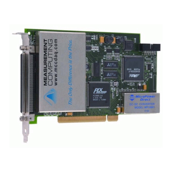
- Page 1 PCI-DAS6052 Analog and Digital I/O Board User’s Guide Document Revision 2, November, 2003 © Copyright 2003, Measurement Computing Corporation...
- Page 2 30 Day Money Back Guarantee Any Measurement Computing Corp. product may be returned within 30 days of purchase for a full refund of the price paid for the product being returned. If you are not satisfied, or chose the wrong product by mistake, you do not have to keep it.
- Page 3 Lifetime Harsh Environment Warranty ™ Any product manufactured by Measurement Computing Corp. that is damaged (even due to misuse) may be replaced for only 50% of the current list price. I/O boards face some tough operating conditionssome more severe than the boards are designed to withstand.
-
Page 5: Table Of Contents
What you will learn from this user's guide..............ix Conventions in this user's guide ....................ix Where to find more information....................x Chapter 1 Introducing the PCI-DAS6052 Series Board........... 1-1 Overview: PCI-DAS6052 features................1-1 Software features–InstaCal and Universal Library ..........1-2 Chapter 2 Installing the Board .................. - Page 6 PCI-DAS6052 User's Guide SCANCLK signal........................4-5 A/D START TRIGGER signal....................4-6 A/D STOP TRIGGER signal....................4-7 STARTSCAN signal ......................4-8 SSH signal ..........................4-9 A/D CONVERT signal......................4-9 A/D PACER GATE signal ....................4-10 A/D EXTERNAL TIME BASE signal ................. 4-10 A/D STOP signal........................
- Page 7 PCI-DAS6052 User's Guide Environmental ......................6-13 Mechanical ........................ 6-13 DAQ-Sync Connector and Pin Out ................6-14 Main Connector and Pin Out..................6-14...
-
Page 9: Preface
About this User's Guide What you will learn from this user's guide This user's guide explains how to install, configure, and use the PCI-DAS6052 so that you get the most out of the analog, digital, and timing I/O features. This user's guide also refers you to related documents available on our web site, and to technical support resources that can also help you get the most out of these boards. -
Page 10: Where To Find More Information
The STC Register Map for the PCI-DAS6000 Series is available on our web site at www.mccdaq.com/registermaps/RegMapSTC6000.pdf. The Specifications: PCI-DAS6052 (the PDF version of Chapter 6 in this guide) is available on our web site at www.mccdaq.com/pdfs/pci-DAS6052.pdf. The Universal Library User's Guide is available on our web site at www.mccdaq.com/PDFmanuals/sm-ul-user-guide.pdf. -
Page 11: Introducing The Pci-Das6052 Series Board
Interrupts can be generated by up to seven ADC sources and four DAC sources. Interrupt sources are listed in Chapter 6 ("Specifications"). The PCI-DAS6052 board contains an 82C54 counter chip, which consists of three 16-bit counters. Clock, gate, and output signals from two of the three counters are available on... -
Page 12: Software Features-Instacal And Universal Library
Introducing the PCI-DAS6052 Series Board Software features–InstaCal and Universal Library The PCI-DAS6052 ships with the InstaCal software utility package. InstaCal is a complete installation, calibration and test program for data acquisition and control boards. Complete with extensive error checking, InstaCal guides you through installation and setup of your data acquisition board and creates the board configuration file for use by your program or application software package. -
Page 13: Installing The Board
As you unpack your board, make sure each of the items shown below is included: Standard components The following items should be included with your shipment: PCI-DAS6052 InstaCal installation CD. If you ordered the optional Universal Library, use that CD to install both InstaCal... -
Page 14: Optional Components
PCI-DAS6052 User's Guide Installing the Board MCC's Software Installation Manual Optional components If you ordered any of the following products with your board, they should be included with your shipment. Universal Library Universal Library™ Data Acquisition and Control Programming Tools (also... -
Page 15: Unpacking The Board
Email: techsupport@measurementcomputing.com Unpacking the board The PCI-DAS6052 boards are shipped in an antistatic container to prevent damage by an electrostatic discharge. To avoid such damage, perform the following procedure when unpacking and handling your board. Before opening the antistatic container, ground yourself with a wrist-grounding strap or by holding onto a grounded object (such as the computer chassis). -
Page 16: Installing The Hardware
PCI-DAS6052 User's Guide Installing the Board Installing the hardware The PCI-DAS6052 board is completely plug-and-play. There are no switches or jumpers to set on the board. Configuration is controlled by your system's BIOS. To install your board, follow the steps below. -
Page 17: Configuring The Hardware
Installing the Board Configuring the hardware All hardware configuration options on the PCI-DAS6052 are software controlled. You can select some of the configuration options using InstaCal, such as the analog input configuration (16 single-ended or eight differential channels), the edge used for triggering when using an external pacer, and the source for the two independent counters. -
Page 18: Non-Referenced Single-Ended Input Mode
PCI-DAS6052 User's Guide Installing the Board Non-referenced single-ended input mode This mode is a compromise between differential and single-ended modes. It offers some of the advantages of each mode. Using non-referenced single-ended mode, you can still get noise rejection, but not the limitation in the number of channels resulting from a fully differential configuration. -
Page 19: Connecting The Board For I/O Operations
Connecting the board for I/O operations Connectors, cables – main I/O connector Table 2-1 lists the board connectors, applicable cables and compatible accessory boards that can be used with the PCI-DAS6052 board. Table 2-1. Board Connectors, Cables, Accessory Equipment Connector type Shielded SCSI 100 D-Type C100HD50-x, unshielded ribbon cable. -
Page 20: Pinout - Main I/O Connector
PCI-DAS6052 User's Guide Installing the Board Signal Name Signal Name Pinout – • • main I/O CTR2 OUT • • AUXIN5 / A/D PACER GATE • • CTR2 GATE AUXIN4 / D/A START TRIGGER connector CTR2 CLK • • AUXIN3 / D/A UPDATE •... - Page 21 PCI-DAS6052 User's Guide Installing the Board Signal Name Signal Name Table 2-3. 16-Channel • • CTR2 OUT • • AUXIN5 / A/D PACER GATE Single-Ended CTR2 GATE • • AUXIN4 / D/A START TRIGGER Mode • • CTR2 CLK AUXIN3 / D/A UPDATE •...
- Page 22 PCI-DAS6052 User's Guide Installing the Board Cabling – main I/O connector Strain relief is stamped “Pins 1-50”. Pins 1-50 are on the long side of the “D” connector. The red stripe identifies pin # 1 Pins 51-100 are on the short side of Strain relief is the “D”...
-
Page 23: Daq-Sync Connector And Pinout
PCI-DAS6052 User's Guide Installing the Board DAQ-Sync Connector and Pinout Table 2- 4. DAQ-Sync Connector and cable types Connector type 14-pin right-angle 100 mil box header Compatible cable MCC p/n: CDS-14-x, 14 pin ribbon cable for board-to board DAQ-Sync connection; x = number of boards (Figure 2-3 shows a CDS-14-3 cable) Table 2-5. -
Page 24: Field Wiring, Signal Termination And Conditioning
Field wiring, signal termination and conditioning You can use the following BNC and screw terminal boards to terminate field signals and route them into the PCI-DAS6052 using the C100HD50-x cable: BNC-16SE – Brings analog signals to standard BNC connectors. Designed for boards operating in single-ended mode. -
Page 25: Programming And Developing Applications
DAS models will not function correctly with your board. Programming languages Measurement Computing’s Universal Library® provides access to board functions from a variety of Windows programming languages. If you are planning to write programs, or ... -
Page 26: Register-Level Programming
PCI-DAS6052 User's Guide Programming and Developing Applications Register-level programming You should use the Universal Library or one of the packaged application programs mentioned above to control your board. Only experienced programmers should try register-level programming. If you need to program at the register level in your application, refer to the STC Register Map for the PCI-DAS6000 Series (available at http://www.measurementcomputing.com/registermaps/RegMapSTC6000.pdf). -
Page 27: Chapter 4 Functional Details
Functional Details Basic architecture Figure 4-1 on page 4-4 is a simplified block diagram of the PCI-DAS6052. This board provides all of the functional elements shown in the figure. The System Timing and Control (STC) is the logical center for all DAQ, DIO, and DAC (if applicable) operations. - Page 28 PCI-DAS6052 User's Guide Functional Details Table 4-1. Auxiliary I/O Signals I/O Type Signal Name Function AUXIN<5:0> A/D CONVERT External ADC Convert Strobe (default) Sources A/D TIMEBASE IN External ADC Pacer Time Base (SW selectable) A/D START TRIGGER ADC Start Trigger (default)
-
Page 29: Daq-Sync Signals
The DAQ-Sync hardware provides the capability of triggering or clocking up to four slave boards from a master board to synchronize data input and/or output. The PCI-DAS6052 board provides the capability of inter-board synchronization between boards in the PCI-DAS6000 family. There are five trigger/strobes and a synchronizing clock provided on a 14-pin header. - Page 30 8-BIT EXT CTR1 CLK CTR1 CLK CTR1 GATE USER COUNTER CTR1 OUT 82C54 LOCAL BUS CTR2 GATE Control USER COUNTER CTR2 OUT Boot EEPROM THRESH-HI 12-BIT PCI BUS (5V, 32-BIT, 33 MHZ) THRESH-LO 12-BIT Figure 4-1. Block Diagram – PCI-DAS6052...
-
Page 31: Daq Signal Timing
PCI-DAS6052 User's Guide Functional Details DAQ signal timing The DAQ timing signals are: SCANCLK A/D START TRIGGER A/D STOP TRIGGER STARTSCAN A/D CONVERT A/D PACER GATE A/D EXTERNAL TIME BASE A/D STOP ATRIG SCANCLK signal SCANCLK is an output signal that may be used for switching external multiplexers. It is a 400 ns wide pulse that follows the CONVERT signal after a 50 ns delay. -
Page 32: A/D Start Trigger Signal
PCI-DAS6052 User's Guide Functional Details A/D START TRIGGER signal Use the A/D START TRIGGER signal for conventional triggering (when you only need to acquire data after a trigger event). Figure 4-3 shows the A/D START TRIGGER signal timing for a conventionally triggered acquisition. -
Page 33: A/D Stop Trigger Signal
PCI-DAS6052 User's Guide Functional Details The A/D START TRIGGER signal is also used to initiate pre-triggered DAQ operations (when you need to acquire data just before a trigger event). In most pre-triggered applications, the A/D START TRIGGER signal is generated by a software trigger. The use of A/D START TRIGGER and A/D STOP TRIGGER in pre-triggered DAQ applications is explained next. -
Page 34: Startscan Signal
PCI-DAS6052 User's Guide Functional Details Rising Edge Polarity Falling Edge Polarity = 37.5 ns minimum Figure 4-7. A/D STOP TRIGGER Input Signal Timing = 50 ns Figure 4-8. A/D STOP TRIGGER Output Signal Timing STARTSCAN signal The STARTSCAN output signal indicates when a scan of channels has been initiated. -
Page 35: Ssh Signal
PCI-DAS6052 User's Guide Functional Details SSH signal The SSH signal can be used as a control signal for external sample/hold circuits. The SSH signal is a programmable polarity pulse that is asserted throughout a channel scan. The state of this signal changes after the start of the last conversion in the scan. The SSH signal may be routed via software selection to any of the AUXOUT pins. -
Page 36: A/D Pacer Gate Signal
PCI-DAS6052 User's Guide Functional Details Rising Edge Polarity Falling Edge Polarity = 37.5 ns minimum Figure 4-11. A/D CONVERT Signal Input Timing Requirement = 50 ns Figure 4-12. A/D CONVERT Signal Output Timing Requirement The A/D CONVERT signal is generated by the on-board pacer circuit unless the external clock option is in use. -
Page 37: A/D Stop Signal
PCI-DAS6052 User's Guide Functional Details =50 ns minimum =23 ns minimum Figure 4-13. A/D EXTERNAL TIME BASE Signal Timing A/D STOP signal The A/D STOP signal indicates a completed acquisition sequence. You can program this signal to be available at any of the AUXOUT pins. The A/D STOP output signal is a 50 ns wide pulse whose leading edge indicates a DAQ done condition. -
Page 38: Atrig Signal
Functional Details ATRIG signal In addition to standard digital trigger features, the PCI-DAS6052 also provides analog triggering capability. When using the analog trigger, acquisitions may be started and controlled via an analog signal. There are four trigger/gate modes available using the analog trigger feature: Trigger –... - Page 39 PCI-DAS6052 User's Guide Functional Details Trigger Above The acquisition will begin when the ATRIG signal first goes above the THRESH_HI. This mode is non-retriggerable. Thresh_HI Trigger Acquired Data Figure 4-15. Trigger Positive Slope 4-13...
- Page 40 PCI-DAS6052 User's Guide Functional Details Trigger Below The acquisition will begin when ATRIG signal fist goes below the THRESH_LO level. This mode is non-retriggerable. Thresh_LO Trigger Acquired Data Figure 4-16. Trigger Negative Slope 4-14...
- Page 41 PCI-DAS6052 User's Guide Functional Details Gate Above Data acquisition is enabled whenever ATRIG goes above the THRESH_HI level. Acquisition is suspended whenever the ATRIG signal goes below the THRESH_HI level. This is a level-sensitive gating mode. Thresh_HI Trigger Result Figure 4-17. Gate Above...
- Page 42 PCI-DAS6052 User's Guide Functional Details Gate Below Data acquisition is enabled whenever ATRIG goes below the THRESH_LO level. Acquisition is suspended whenever the ATRIG signal goes above the THRESH_LO level. This is a level-sensitive gating mode. Thresh_LO Trigger Acquired Data Figure 4-18.
- Page 43 PCI-DAS6052 User's Guide Functional Details Gate Negative Hysteresis Data acquisition is enabled whenever ATRIG goes above the THRESH_HI level. Acquisition is suspended whenever the ATRIG signal goes below the THRESH_LO level. The hysteresis level is set by THRESH_LO. This is a level-sensitive gating mode.
- Page 44 PCI-DAS6052 User's Guide Functional Details Gate Positive Hysteresis Data acquisition is enabled whenever ATRIG goes below the THRESH_LO level. Acquisition is suspended whenever the ATRIG signal goes above the THRESH_HI level. The hysteresis level is set by THRESH_HI. This is a level-sensitive gating mode.
- Page 45 PCI-DAS6052 User's Guide Functional Details Gate Inside Window Data acquisition is enabled whenever ATRIG is below the THRESH_HI level and above the THRESH_LO level. Acquisition is suspended whenever the ATRIG signal is outside of this region. This is a level-sensitive gating mode...
- Page 46 PCI-DAS6052 User's Guide Functional Details Gate Outside Window Data acquisition is enabled whenever ATRIG is above the THRESH_HI level or below the THRESH_LO level. Acquisition is suspended whenever the ATRIG signal is between the THRESH_HI and THRESH_LO levels. This is a level-sensitive gating...
-
Page 47: Waveform Generation Timing Signals
PCI-DAS6052 User's Guide Functional Details Waveform generation timing signals The signals that control the timing for the analog output functions on the PCI-DAS6052 are: D/A START TRIGGER D/A UPDATE D/A EXTERNAL TIME BASE D/A START TRIGGER signal The D/A START TRIGGER signal is used to hold off output scans until after a trigger event. -
Page 48: D/A Convert Signal
PCI-DAS6052 User's Guide Functional Details = 50 ns Figure 4-24. D/A START TRIGGER Output Signal Timing D/A CONVERT signal The D/A CONVERT signal causes a single output update on the D/A converters. You can program the DAQ-Sync DS D/A UPDATE input or any AUXIN pin to accept the D/A CONVERT signal. -
Page 49: D/A External Time Base Signal
PCI-DAS6052 User's Guide Functional Details D/A EXTERNAL TIME BASE signal The D/A EXTERNAL TIME BASE signal can serve as the source for the on-board DAC pacer circuit rather than using the internal time base. Any AUXIN pin can be set programmatically as the source for this signal. -
Page 50: Ctr1 Clk Signal
PCI-DAS6052 User's Guide Functional Details CTR1 CLK signal The CTR1 CLK signal can serve as the clock source for independent user counter 1. It can be selected through software at the CTR1 CLK pin rather than using the on-board 10 MHz or 100 kHz sources. It is also polarity programmable. The maximum input frequency is 10 MHz. -
Page 51: Ctr1 Out Signal
PCI-DAS6052 User's Guide Functional Details CTR1 OUT signal This signal is present on the CTR1 OUT pin. The CTR1 OUT signal is the output of one of the two user’s counters in an industry-standard 82C54 chip. For detailed information on counter operations, please refer to the data sheet on our WEB page at http://www.measurementcomputing.com/PDFmanuals/82C54.pdf. -
Page 52: Ctr2 Gate Signal
PCI-DAS6052 User's Guide Functional Details CTR2 GATE signal You can use the CTR2 GATE signal for starting and stopping the counter, saving counter contents, etc. It is polarity programmable and is available at the CTR2 GATE pin. Figure 4-32 shows the timing requirements for the CTR2 GATE signal. -
Page 53: Calibrating The Board
Chapter 5 Calibrating the Board Introduction You should calibrate the board (using the InstaCal utility) after the board has fully warmed up. The recommended warm-up time is 15 minutes. For best results, calibrate the board immediately before making critical measurements. The high resolution analog components on the board are somewhat sensitive to temperature. - Page 54 PCI-DAS6052 User's Guide Calibrating the Board A similar method is used to calibrate the analog output components. A trim DAC is used to adjust the gain of the DAC. A separate DAC is used to adjust offset on the final output amplifier.
-
Page 55: Chapter 6 Specifications
Chapter 6 Specifications Analog Input Section A/D converter Successive Approximation type, 333kS/s conversion rate. Resolution 16 bits, 1 in 65536 Maximum Sample Rate 333kS/s Number of channels 16 single ended / 8 differential, software selectable Bipolar: ±10V, ±5V, ±2.5V, ±1V, ±0.5V, ±0.25V, ±0.1V, ±0.05V, Input ranges Unipolar:... -
Page 56: Accuracy
PCI-DAS6052 User's Guide Specifications Accuracy 333 kS/s sampling rate, single channel operation and a 15-minute warm-up. Accuracies listed are for measurements made following an internal calibration. They are valid for operational temperatures within ±1°C of internal calibration temperature and ±10°C of factory calibration temperature. - Page 57 PCI-DAS6052 User's Guide Specifications Table 6-2. Absolute Accuracy Components – All values are (±) Noise +Quantization Absolute Temp Drift % of Offset (µV) Range Accuracy at Reading (µV) (%/DegC) FS (mV) Single Pt Averaged ±10V 0.0371 87.0 0.0006 4.747 ±5V 0.0071...
- Page 58 PCI-DAS6052 User's Guide Specifications Each PCI-DAS6052 is tested at the factory to assure the board’s overall error does not exceed accuracy limits described in Table 6-1on page 6-2. Table 6-3. Relative Accuracy – All values are (±) Relative Accuracy (µV)
-
Page 59: Settling Time
PCI-DAS6052 User's Guide Specifications Settling Time Settling time is defined as the time required for a channel to settle to within a specified accuracy in response to a full-scale (FS) step. Two channels are scanned at the specified rate. A –FS DC signal is presented to Channel 1; a +FS DC signal is presented to Channel 0. -
Page 60: Parametrics
PCI-DAS6052 User's Guide Specifications Parametrics Max working voltage ±11V (signal + common-mode) ±10V Range: 92dB 0 to 10V & ±5V Range: 97dB 0 to 5V & ±2.5V Range: 101dB 0 to 2V & ±1V Range: 104dB CMRR @ 60Hz 0 to 1V & ±0.5V Range: 105dB 0 to 0.5V &... -
Page 61: Noise Performance
Specifications Noise Performance Table 6-5 summarizes the noise performance for the PCI-DAS6052. Noise distribution is determined by gathering 50K samples with inputs tied to ground at the user connector. Samples are gathered at the maximum specified single channel sampling rate. -
Page 62: Analog Output Section
0.0001 1.405 0 to 10V 0.0061 0.0001 1.176 Each PCI-DAS6052 is tested at the factory to assure the board’s overall error does not exceed the values specified in Table 6-6. Table 6-8. Relative Accuracy Range Relative Accuracy All Ranges ±0.35 LSB, typical ±1.0 LSB, max... -
Page 63: Analog Output Pacing And Triggering
PCI-DAS6052 User's Guide Specifications Analog Output Pacing and Triggering Internal counter – ASIC. Selectable time base: Internal 40MHz, 50ppm stability. DAC pacing External Source via AUXIN<5:0>, SW selectable. (SW programmable) External convert strobe: D/A UPDATE Software paced External digital: D/A START TRIGGER... -
Page 64: Analog Trigger
PCI-DAS6052 User's Guide Specifications Analog Trigger Analog Trigger Sources External: ATRIG input Software selectable CH0 IN through CH15 IN, first channel in scan ATRIG input: ±10V Analog Trigger Levels CH0 IN through CH15 IN: ± Full-scale, range dependent External analog: Software-configurable for:... -
Page 65: Interrupt Section
PCI-DAS6052 User's Guide Specifications Interrupt Section Interrupts PCI INTA# - mapped to IRQn via PCI BIOS at boot-time Interrupt enable Programmable through PLX9080 DAQ_ACTIVE: Interrupt is generated when a DAQ sequence is active. DAQ_STOP: Interrupt is generated when A/D Stop Trigger In is detected. -
Page 66: Configurable Auxin<5:0>, Auxout<2:0> External Trigger/Clocks
PCI-DAS6052 User's Guide Specifications Configurable AUXIN<5:0>, AUXOUT<2:0> External Trigger/Clocks The PCI-DAS6052 provides nine user-configurable Trigger/Clock pins available at the 100-pin I/O connector. Of these, six are configurable as inputs while three are configurable as outputs. A/D CONVERT: External ADC convert strobe... -
Page 67: Daq-Sync Inter-Board Triggers/Clocks
PCI-DAS6052 User's Guide Specifications DAQ-Sync inter-board Triggers/Clocks The DAQ-Sync bus provides inter-board triggering and synchronization capability. Five trigger/strobe I/O pins and one clock I/O pin are provided on a 14-pin header. The DAQ-Sync signals use dedicated pins. Only the direction may be set. -
Page 68: Main Connector And Pin Out
PCI-DAS6052 User's Guide Specifications DAQ-Sync Connector and Pin Out Connector type 14-Pin right-angle 100mil box header Compatible cables MCC p/n: CDS-14-x, 14 pin ribbon cable. x = number of boards (2 - 5) Signal Name DS A/D START TRIGGER DS A/D STOP TRIGGER... - Page 69 PCI-DAS6052 User's Guide Specifications 8 Channel Differential Mode Signal Name Signal Name LLGND CH0 IN HI CH0 IN LO CH1 IN HI CH1 IN LO CH2 IN HI CH2 IN LO CH3 IN HI CH3 IN LO CH4 IN HI...
- Page 70 PCI-DAS6052 User's Guide Specifications 16-Channel Single-Ended Mode Signal Name Signal Name LLGND CH0 IN CH8 IN CH1 IN CH9 IN CH2 IN CH10 IN CH3 IN CH11 IN CH4 IN CH12 IN CH5 IN CH13 IN CH6 IN CH14 IN...
- Page 71 EC Declaration of Conformity We, Measurement Computing Corporation, declare under sole responsibility that the products PCI-DAS6052 High speed analog and digital I/O board for the PCI bus. Part Number Description to which this declaration relates, meets the essential requirements, is in conformity with,...
- Page 72 Measurement Computing Corporation 16 Commerce Boulevard, Middleboro, Massachusetts 02346 (508) 946-5100 Fax: (508) 946-9500 E-mail: info@mccdaq.com www.mccdaq.com...
Need help?
Do you have a question about the PCI-DAS6052 and is the answer not in the manual?
Questions and answers