
Subscribe to Our Youtube Channel
Related Manuals for SMART Embedded Computing MVME4100


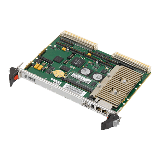
Summary of Contents for SMART Embedded Computing MVME4100
- Page 1 MVME4100 Single Board Computer Programmer’s Reference P/N: 6806800H19D September 2019...
- Page 2 Computing” and the SMART Embedded Computing logo are trademarks of SMART Modular Technologies, Inc. All other names and logos referred to are trade names, trademarks, or registered trademarks of their respective owners. These materials are provided by SMART Embedded Computing as a service to its customers and may be used for informational purposes only. Disclaimer* SMART Embedded Computing (SMART EC) assumes no responsibility for errors or omissions in these materials.
-
Page 3: Table Of Contents
3.1.17 Watch Dog Timer Load Register ........39 MVME4100 Single Board Computer Programmer’s Reference (6806800H19D) - Page 4 4.13.3 Local Bus Controller Clock Divisor........64 MVME4100 Single Board Computer Programmer’s Reference (6806800H19D)
- Page 5 Related Documentation ............79 B.1 SMART Embedded Computing Documentation ....... . . 79 B.2 Manufacturers’...
- Page 6 Table of Contents MVME4100 Single Board Computer Programmer’s Reference (6806800H19D)
- Page 7 Boot Flash Bank ..........30 MVME4100 Single Board Computer Programmer’s Reference (6806800H19D)
- Page 8 Table of Contents MVME4100 Single Board Computer Programmer’s Reference (6806800H19D)
- Page 9 Tick Timer Counter Register ..........46 MVME4100 Single Board Computer Programmer’s Reference (6806800H19D)
- Page 10 Related Specifications ..........81 MVME4100 Single Board Computer Programmer’s Reference (6806800H19D)
-
Page 11: About This Manual
This manual is divided into the following chapters and appendices: Chapter 1, Introduction on page 15, provides a brief product description and a block diagram showing the architecture of the MVME4100 Single Board Computer. Chapter 2, Memory Maps on page 21, provides information on the board’s memory maps. -
Page 12: Table 1 Conventions Table
Repeated item for example node 1, node 2, ..., node 12 Omission of information from example/command that is not necessary at the time Ranges, for example: 0..4 means one of the integers 0,1,2,3, and 4 (used in registers) Logical OR MVME4100 Single Board Computer Programmer’s Reference (6806800H19D) - Page 13 Indicates an electrical situation that could result in moderate injury or death Indicates that when working in an ESD environment care should be taken to use proper ESD practices No danger encountered, pay attention to important information MVME4100 Single Board Computer Programmer’s Reference (6806800H19D)
- Page 14 Timing Parameters" and "Variable VPD Contents", added information on MRAM, real time clock and Quad UART, removed "Serial Presence Detect Checksum Calculation" and "SPD Contents for MVME4100 Boards", editorial changes 6806800H19A January 2009 Early access version MVME4100 Single Board Computer Programmer’s Reference (6806800H19D)
-
Page 15: Introduction
Board Computer. Refer to the MPC8548E Reference Manual listed in Appendix B, Related Documentation, for more detail and programming information. At the time of publication of this manual, the MVME4100 is available in the configurations shown below. Table 1-1 Board Variants... - Page 16 One quad UART (QUART) controller to provide four 16550- compatible, 9.6 to 115.2 Kbaud, asynchronous serial channels: four channels for rear P2 I/O Timers Four 32-bit MPC8548E timers Four 32-bit timers in a PLD Watchdog Timer One watchdog timer in PLD MVME4100 Single Board Computer Programmer’s Reference (6806800H19D)
- Page 17 Planar status indicators One standard 16-pin COP header One standard 20-pin JTAG header Boundary scan support Switches for VME geographical addressing in a three-row backplane Software Support VxWorks OS support Linux OS support MVME4100 Single Board Computer Programmer’s Reference (6806800H19D)
-
Page 18: Block Diagram
Introduction Introduction Block Diagram The following figure is a block diagram of the MVME4100 architecture. Figure 1-1 Block Diagram MVME4100 Single Board Computer Programmer’s Reference (6806800H19D) -
Page 19: Functional Description
Functional Description The MVME4100 VMEbus board is based on the MPC8548E system-on-chip (SoC) processor. The MVME4100 provides front panel access to one serial port with a micro DB-9 connector, two 10/100/1000 Ethernet ports with two RJ-45 connectors, and one USB port with one type A connector. - Page 20 Introduction Introduction MVME4100 Single Board Computer Programmer’s Reference (6806800H19D)
-
Page 21: Memory Maps
Chapter 2 Memory Maps Overview The following sections describe the memory maps for the MVME4100. Refer to the MPC8548E Reference Manual for additional details and/or programming information. 2.1.1 Default Processor Memory Map The following table describes a default memory map from the point of view of the processor after a processor reset. -
Page 22: Pci Memory Map
- 1 dram_size System Memory (on-board DRAM) 2.1.4 VME Memory Map The MVME4100 is fully capable of supporting both the PReP and the CHRP VME Memory Map examples with RAM size limited to 2GB. MVME4100 Single Board Computer Programmer’s Reference (6806800H19D) -
Page 23: Register Descriptions
System resources including system control and status registers, external timers, and the QUART are mapped into a 16 MB address range accessible from the MVME4100 local bus via the MPC8548E LBC. The memory map is defined in the following table including the LBC bank chip select used to decode the register. -
Page 24: Table 3-18 Nand Flash Chip 2 Presence Register
Reserved (32 bits) F200 002C Reserved (32 bits) F200 0030 PLD Revision F200 0031 Reserved F200 0032 Reserved F200 0033 Reserved F200 0034 PLD Date Code (32 bits) F200 0038 Test Register 1 (32 bits) MVME4100 Single Board Computer Programmer’s Reference (6806800H19D) -
Page 25: Table 3-27 Test Register 2
External PLD Tick Timer 3 Control Register F202 0034 External PLD Tick Timer 3 Compare Register F202 0038 External PLD Tick Timer 3 Counter Register F202 003C Reserved F202 0040 External PLD Tick Timer 4 Control Register MVME4100 Single Board Computer Programmer’s Reference (6806800H19D) -
Page 26: System Status Register
2. 32-bit write only. 3. Byte read/write capable. 3.1.1 System Status Register The MVME4100 has a System Status Register that is a read only register used to provide general board status information. Table 3-2 System Status Register System Status Register - 0xF200 0000... -
Page 27: System Control Register
A set condition indicates the switch is on. 3.1.2 System Control Register The MVME4100 has a System Control Register that provides general board control bits. Table 3-3 System Control Register System Control Register - 0xF200 0001... -
Page 28: Status Indicator Register
3.1.3 Status Indicator Register The MVME4100 provides a Status Indicator Register that may be read by the system software to determine the state of the on-board status indicator LEDs or written to by system software to illuminate the corresponding on-board LEDs. -
Page 29: Nor Flash Control/Status Register
Memory Map Select. When this bit is cleared, the flash memory map is controlled by the Flash Boot Block Select switch (see the MVME4100 Installation and Use manual for switch settings). When the Map Select bit is set, boot block A is... -
Page 30: Interrupt Register 1
Figure 3-1 Boot Flash Bank 3.1.5 Interrupt Register 1 The MVME4100 provides an Interrupt Register that may be read by the system software to determine which of the Ethernet PHYs originated their combined (OR'd) interrupt Table 3-6 Interrupt Register 1... -
Page 31: Interrupt Register 2
3.1.6 Interrupt Register 2 The RTC, TEMP sensor and Abort switch interrupts are OR'd together. The MVME4100 provides an Interrupt Register that may be read by the system software to determine which device originated the interrupt. This register also includes bits that allow the interrupt sources to be mask. -
Page 32: Presence Detect Register
Register Descriptions Register Descriptions 3.1.7 Presence Detect Register The MVME4100 provides a Presence Detect Register that may be read by the system software to determine the presence of optional devices. Table 3-8 Presence Detect Register Presence Detect Register - 0xF200 0006... -
Page 33: Table 3-10 Pci Bus 2 Status Register
5.0V VIO Enabled. This bit set indicates that the PMC bus (PCI Bus 2) is configured for 5.0V VIO. 3.3V_VIO 3.3V VIO Enabled. This bit set indicates that the PMC bus (PCI Bus 2) is configured to 3.3V VIO. MVME4100 Single Board Computer Programmer’s Reference (6806800H19D) -
Page 34: Nand Flash Chip 1 Control Register
RSVD Reserved for future implementation. 3.1.9 NAND Flash Chip 1 Control Register The MVME4100 provides a Control Register for the NAND Flash device. Table 3-12 NAND Flash Chip 1 Control Register NAND Flash Chip 1 Control Register - 0xF200 0010... -
Page 35: Nand Flash Chip 1 Select Register
RSVD Reserved for future implementation. 3.1.10 NAND Flash Chip 1 Select Register The MVME4100 provides a Select Register for the NAND Flash device. Table 3-13 NAND Flash Chip 1 Select Register NAND Flash Chip 1 Select Register - 0xF200 0011... -
Page 36: Nand Flash Chip 1 Presence Register
Register Descriptions Register Descriptions 3.1.11 NAND Flash Chip 1 Presence Register The MVME4100 provides a Presence Register for the NAND Flash device. Table 3-14 NAND Flash Chip 1 Presence Register NAND Flash Chip 1 Presence Register - 0xF200 0014 Field... -
Page 37: Nand Flash Chip 2 Control Register
Register Descriptions 3.1.13 NAND Flash Chip 2 Control Register The MVME4100 provides a Control Register for the NAND Flash device. Table 3-16 NAND Flash Chip 2 Control Register NAND Flash Chip 2 Control Register - 0xF200 0018 Field RSVD RSVD... -
Page 38: Nand Flash Chip 2 Presence Register
RSVD Reserved for future implementation. 3.1.15 NAND Flash Chip 2 Presence Register The MVME4100 provides a Presence Register for the NAND Flash device. Table 3-18 NAND Flash Chip 2 Presence Register NAND Flash Chip 2 Presence Register - 0xF200 001C... -
Page 39: Nand Flash Chip 2 Status Register
Register Descriptions 3.1.16 NAND Flash Chip 2 Status Register The MVME4100 provides a Status Register for the NAND Flash device. Table 3-19 NAND Flash Chip 2 Status Register NAND Flash Chip 2 Status Register - 0xF200 001D Field RSVD RSVD... -
Page 40: 3.1.18 Watch Dog Control Register
SYSRST System Reset. If cleared a board-level reset is generated when a time-out occurs. If set, a VMEbus SYSRST is generated when a time-out occurs. If MVME4100 is SYSCON then a local reset will also result in a VMEbus SYSRST. -
Page 41: 3.1.20 Watch Dog Timer Count Register
32 ms 64 ms RSVD Reserved for future implementation. 3.1.20 Watch Dog Timer Count Register The MVME4100 provides a watch dog timer count register. Table 3-23 Watch Dog Timer Count Register Watch Dog Timer Counter Register - 0xF200 0026 15:0 Field... -
Page 42: Pld Revision Register
Register Descriptions Register Descriptions 3.1.21 PLD Revision Register The MVME4100 provides a PLD revision register that can be read by the system software to determine the current revision of the timers/registers PLD. Table 3-24 PLD Revision Register PLD Revision Register - 0xF200 0030... -
Page 43: Test Register 1
TEST1 General purpose 32-bit R/W field. 3.1.24 Test Register 2 The MVME4100 provides a second 32-bit test register that reads back the complement of the data in Test Register 1. Table 3-27 Test Register 2 Test Register 2 - 0xF200 003C... -
Page 44: External Timer Registers
3.1.25 External Timer Registers The MVME4100 provides a set of tick timer registers for access to the four external timers implemented in the timers/registers PLD. Note that these registers are 32-bit registers and are not byte writable. The following sections describe the external timer prescaler and control registers. -
Page 45: 3.1.25.2 Control Registers
If the clear-on-compare mode is enabled the counter is also cleared. For periodic interrupts this equation should be used to calculate the compare register value for a specific period (T): MVME4100 Single Board Computer Programmer’s Reference (6806800H19D) -
Page 46: 3.1.25.4 Counter Register
The VMEbus Status Register in the Tsi148 provides the VMEbus geographical address of the MVME4100. This register reflects the inverted states of the geographical address pins at the 5-row, 160-pin P1 connector. Applications not using the 5-row backplane can use the planar switch described in the MVME4100 Installation and Use manual to assign a geographical address. -
Page 47: Programming Details
Clock Distribution on page 62 MPC8548E Reset Configuration The MVME4100 supports the power-on reset (POR) pin sampling method for processor reset configuration. The states of the various configuration pins on the processor are sampled when reset is deasserted to determine the desired operating modes. - Page 48 PCI-X mode configuration PCI mode EC_MDC Fixed TSEC 1 and 2 TSEC 1 and 2 in reduced width mode (RTBI or RGMII) configuration TSEC 1 and 2 in standard mode (TBI or GMII) MVME4100 Single Board Computer Programmer’s Reference (6806800H19D)
- Page 49 TSEC1_TCD[6:4 Fixed Boot ROM PCI1/PCI-X location DRR SDRAM PCI2 Serial Rapid IO PCI Express Local bus GPCM- 8-bit ROM Local bus GPCM - 16-bit Local bus GPCM - 32-bit MVME4100 Single Board Computer Programmer’s Reference (6806800H19D)
- Page 50 TSEC2 controller uses GMII protocol (RGMII if TSEC2 configured in reduced mode) TSEC2 controller uses TBI protocol (RTBI if TSEC2 configured in reduced mode) TSEC2_TXD[1, Fixed DDR DRAM Reserved TSEC2_RX_ER] type DDR1 Reserved DDR2 MVME4100 Single Board Computer Programmer’s Reference (6806800H19D)
- Page 51 Fixed SerDes enable 0 SerDes interface is disabled SerDes interface is enabled LA[27] Fixed CPU boot CPU boot hold off mode configuration e500 core boots without waiting for configuration by an external master MVME4100 Single Board Computer Programmer’s Reference (6806800H19D)
- Page 52 Agent of a RapidIO; host PCI Express and PCI1/PCI-x Endpoint PCI Express; host RapidIO and PCI/PCI-X Reserved Agent PCI1/PCI-X and RapidIO; root complex PCI Express Agent PCI1/PCI-X; host RapidIO; root complex PCI Express Host processor/root complex MVME4100 Single Board Computer Programmer’s Reference (6806800H19D)
- Page 53 Debug info from the DDR SDRAM controller is driven on MSRCID and MDVAL pins MSRCID1 Fixed DDR debug Debug info on ECC pins configuration instead of normal ECC ECC pins function in normal mode MVME4100 Single Board Computer Programmer’s Reference (6806800H19D)
-
Page 54: Mpc8548E Interrupt Controller
Programming Details Programming Details MPC8548E Interrupt Controller The MVME4100 uses the MPC8548E integrated programmable interrupt controller (PIC) to manage locally generated interrupts. Currently defined external interrupting devices and interrupt assignments, along with corresponding edge/levels and polarities, are shown in the following table. -
Page 55: Local Bus Controller Chip Select Assignments
1. Flash bank size determined by VPD flash packet. 2. Control/Status registers are byte read and write capable. 3. 32-bit timer registers are byte readable, but must be written as 32 bits. 4. MRAM is byte read and write capable. MVME4100 Single Board Computer Programmer’s Reference (6806800H19D) -
Page 56: I2C Device Addresses
C controller is used by the system software to read the contents of the various I C devices located on the MVME4100. The following table contains the I C devices used for the MVME4100 and their assigned device addresses. Table 4-4 I2C Bus Device Addressing Device... -
Page 57: Vpd Eeprom
Programming Details VPD EEPROM The MVME4100 board provides an 8 KB dual address serial EEPROM containing Vital Product Data (VPD) configuration information specific to the MVME4100. Typical information that may be present in the EEPROM may include: manufacturer, board revision, build version, date of assembly, memory present, options present, L2 cache information, etc. -
Page 58: Flash Memory
4.10 Flash Memory The MVME4100 is designed to provide 128 MB of soldered-on NOR flash memory. Two +3.0 V devices are configured to operate in 16-bit mode to form a 32-bit flash bank. This flash bank is also the boot bank and is connected to LBC Chip Select 0 and 1. The NOR flash is accessed via the MPC8548E local bus. -
Page 59: Pci Idsel And Interrupt Definition
IRQ6 IRQ7 IRQ4 IRQ5 Primary 0b0_0011 PMC2 IRQ7 IRQ4 IRQ5 IRQ6 Secondary PCI2 0b0_0010 uPD720101 IRQ4 IRQ5 IRQ6 (PCI6520) Refer to the MPC8548E reference manual for additional details about the MPC8548E PIC operation. MVME4100 Single Board Computer Programmer’s Reference (6806800H19D) -
Page 60: Pci Arbitration Assignments
PCI Arbitration Assignments The integrated PCI/X arbiters internal to the PLX PCI6520 provide PCI arbitration for the MVME4100. The arbitration assignments on the MVME4100 are shown in the next table so that software may set arbiter priority assignments if necessary. Table 4-10... -
Page 61: Other Software Considerations
4.12.1 MRAM The MVME4100 provides 512 K bytes of fast non-volatile storage in the form of MRAM (Magnetoresistive Random Access Memory). The MRAM is directly accessible by software in the same manner as the DRAM (that means using processor load and store instructions). -
Page 62: Lbc Timing Parameters
X bus clocks are generated using a MPC9855 clock generator. Additional clocks required by individual devices are generated near the devices using individual oscillators. The following table lists the clocks required on the MVME4100 along with their frequency and source. -
Page 63: System Clock
The RTC clock input is driven by 1 MHz clock generated by the Control and Timers PLD. This provides a fixed clock reference for the MPC8548E PIC timers which software can use as a known timing reference. MVME4100 Single Board Computer Programmer’s Reference (6806800H19D) -
Page 64: Local Bus Controller Clock Divisor
Programming Details Programming Details 4.13.3 Local Bus Controller Clock Divisor The Local Bus Controller (LBC) clock output is connected to the PLD but is not used by the internal logic. MVME4100 Single Board Computer Programmer’s Reference (6806800H19D) -
Page 65: Programmable Configuration Data
Programmable Configuration Data Overview This appendix provides data and specifications pertaining to programmable parts used on the MVME4100. The board is shipped after the programmable parts have been programmed through ATE or boundary scan according to the In-Circuit Test specifications. Table A-1... -
Page 66: Vital Product Data (Vpd) Introduction
The firmware ignores the VPD contents and attempts to acquire information from other sources. Some device drivers will not work. Some diagnostic tests will fail. The board will run much slower than usual. MVME4100 Single Board Computer Programmer’s Reference (6806800H19D) -
Page 67: How To Fix Corrupted Vpd Information
If you suspect that your board has problems, as a result of wrong VPD information, select SAFE mode by setting S1:1 ON and reboot the MVME4100. At this point, the firmware will ignore all SROM contents. Use SROM or the IBM command to change the VPD to the correct parameters. - Page 68 ^= 0x04c11db6; crcValue |= 1; dataByte >>= 1; crcValueFlipped = 0; for (index = 0; index < 32; index++) crcValueFlipped <<= 1; dataBitValue = crcValue & 1; crcValue >>= 1; crcValueFlipped += dataBitValue; MVME4100 Single Board Computer Programmer’s Reference (6806800H19D)
-
Page 69: A.10 Vpd Contents For Mvme4100 Boards
EEPROM. 512 bytes in this VPD architecture BINARY VPD Revision Packet BINARY # of Bytes BINARY Board Type: Processor Board BINARY Architecture Revision BINARY Board Build Revision BINARY Revision Reason Flags MVME4100 Single Board Computer Programmer’s Reference (6806800H19D) - Page 70 Product Identifier Packet BINARY Refer to Notes 1 and 2. BINARY # of bytes Product Identifier. ASCII Table A-4 Refer to Factory Assembly Number. BINARY Refer to Notes 1 and 2. BINARY # of bytes MVME4100 Single Board Computer Programmer’s Reference (6806800H19D)
- Page 71 **Serial number to be filled in. BINARY Refer to Notes 2 and 3. BINARY # of bytes Most significant serial number character ASCII Least significant serial number character BINARY External Processor Clock Frequency Packet BINARY # of bytes MVME4100 Single Board Computer Programmer’s Reference (6806800H19D)
- Page 72 Ethernet Controller 0 BINARY Ethernet MAC Address Packet BINARY # of bytes BINARY Six bytes containing the next Ethernet address. BINARY Ethernet Controller 1 BINARY Ethernet MAC Address Packet BINARY # of bytes MVME4100 Single Board Computer Programmer’s Reference (6806800H19D)
- Page 73 Ethernet MAC Address Packet BINARY # of bytes BINARY Six bytes containing the highest Ethernet address. BINARY Ethernet Controller 3 BINARY Processor Identifier Packet BINARY # of bytes Processor type ASCII Table A-4 Refer to MVME4100 Single Board Computer Programmer’s Reference (6806800H19D)
- Page 74 Column width in bits BINARY Minimum write/erase data width in bits BINARY Flash bank number BINARY Flash access speed in nanoseconds: 0x6E = 110 ns Total bank size [(1<<n)*256K bytes]: 0x09 = 128 BINARY MVME4100 Single Board Computer Programmer’s Reference (6806800H19D)
- Page 75 For this reason, these packets shall have fixed sizes and shall immediately follow the header. 3. This data is not static. Each board's Serial Number packet must be unique. The board's serial number is obtained from the onboard serial number label. MVME4100 Single Board Computer Programmer’s Reference (6806800H19D)
-
Page 76: Table A-4 Variable Vpd Contents
Programmable Configuration Data Programmable Configuration Data The XX in Table A-4 at address 0x32 represents the assembly revision letter (A=41, B=42, etc.). Table A-4 Variable VPD Contents Offset (Hex) MVME4100-0171 MVME4100-0173 0106855E03x 0106855E04x MVME4100 Single Board Computer Programmer’s Reference (6806800H19D) - Page 77 Programmable Configuration Data Table A-4 Variable VPD Contents (continued) Offset (Hex) MVME4100-0171 MVME4100-0173 0106855E03x 0106855E04x MVME4100 Single Board Computer Programmer’s Reference (6806800H19D)
- Page 78 Programmable Configuration Data Programmable Configuration Data MVME4100 Single Board Computer Programmer’s Reference (6806800H19D)
-
Page 79: Related Documentation
SMART EC Publications Document Title Publication Number MVME4100 Data Sheet MVME4100-DS MVME4100 Single Board Computer Installation and Use 6806800H18 MOTLoad Firmware Package User’s Manual 6806800C24 Manufacturers’ Documents For additional information, refer to the following table for manufacturers’ data sheets or user’s manuals. - Page 80 3.0V to 5.5V, 250kbps,RS-232 Transceivers with Auto Shutdown 10/03 MAX811/MAX812 19-0411 4-Pin µP Voltage Monitors Rev 3 With Manual Reset Input 3/99 19-2450 MAX6649 Digital Temperature Sensor Rev 3 05/07 Tundra Semiconductor Corporation MVME4100 Single Board Computer Programmer’s Reference (6806800H19D)
-
Page 81: Related Specifications
Increased Current Level for 96 pin & 160 pin DIN/IEC Connector ANSI/VITA 1.7 Standard Processor PMC ANSI/VITA 32-2003 PCI-X on PMC ANSI/VITA 39-2003 VITA 36 PMC I/O Module (PIM) Draft Standard Draft Rev 0.1 July 19, 1999 Universal Serial Bus MVME4100 Single Board Computer Programmer’s Reference (6806800H19D) - Page 82 Institute for Electrical and Electronics Engineers, Inc. IEEE Standard for a Common Mezzanine Card Family: CMC Family IEEE Std 1386 - 2001 IEEE Standard Physical and Environmental Layer for PCI Mezzanine IEEE Std 1386.1 - 2001 Cards (PMC) MVME4100 Single Board Computer Programmer’s Reference (6806800H19D)
- Page 84 © 2019 SMART Embedded Computing™, Inc. All rights reserved. The stylized “S” and “SMART” is a registered trademark of SMART Modular Technologies, Inc. and “SMART Embedded Computing” and the SMART Embedded Computing logo are trademarks of SMART Modular Technologies, Inc. All other names and logos...
Need help?
Do you have a question about the MVME4100 and is the answer not in the manual?
Questions and answers