
Related Manuals for Xycom XVME-653


Summary of Contents for Xycom XVME-653
- Page 1 XVME-653/658 Single-Slot VMEbus ® ® Intel Pentium /AMD-K6 Processor Module P/N 74653-001B 1999 XYCOM™ AUTOMATION, INC. Printed in the United States of America...
- Page 2 This document is copyrighted by Xycom Automation, Incorporated (Xycom Automation) and shall not be reproduced or copied without expressed written authorization from Xycom Automation. The information contained within this document is subject to change without notice. Xycom Automation does not guarantee the accuracy of the information. Xycom Automation, Inc.
- Page 3 WARNING This is a Class A product. In a domestic environment this product may cause radio in- terference, in which case the user may be required to take adequate measures. European Union Directive 89/336/EEC requires that this apparatus comply with relevant ITE EMC standards.
-
Page 5: Table Of Contents
Table of Contents Table of Contents Chapter 1 – Introduction ................... 1-1 Module Features ........................1-1 Architecture ..........................1-2 CPU Chip ..........................1-2 Ethernet Controller......................... 1-2 PCI Local Bus Interface ......................1-2 Video Controller........................1-2 Fast IDE controller and Floppy Drive Controller..............1-2 VMEbus Interface ........................ - Page 6 P2 Connector ........................2-11 Interboard Connector 1 (P4) ....................2-12 Interboard Connector 2 (P3) ....................2-13 Installing the XVME-653/658 into a Backplane ..............2-14 Enabling the PCI Ethernet Controller..................2-17 Loading the Ethernet Driver ....................2-17 Pinouts for the RJ-45 10/100 BaseT Connector ..............2-17 Using a DiskOnChip .......................
- Page 7 Table of Contents PCI BIOS Functions ......................... 4-6 Calling Conventions....................... 4-7 16-Bit Interface........................4-7 32-Bit Interface........................4-7 PCI BIOS Function Calls ....................... 4-8 Locating the Universe Chip....................4-8 Read Configuration Byte..................... 4-9 Read Configuration Word ....................4-9 Read Configuration Dword ....................4-10 Write Configuration Byte ....................
-
Page 9: Chapter 1 - Introduction
IBM PC standard. These modules inte- grate the latest processor and chipset technology. ® At the core of the XVME-653 is an Intel 233 MHz Pentium CPU with MMX technol- ogy. This generation of Pentium processors features enhanced multimedia instructions, larger level 1 caches, and a 10 to 20 percent performance increase over standard Pentium processors. -
Page 10: Architecture
This section describes the XVME-653/658 processor modules’ architecture. CPU Chip The XVME-653 supports the Intel 233 MHz Pentium MMX processor. The MMX proc- essor features new instructions to improve multimedia performance. A dynamic branch prediction unit, improved internal pipelines, and separate 16 KB data and instruction caches further enhance performance. -
Page 11: Vmebus Interface
VMEbus Interface The XVME-653/658 uses the PCI local bus to interface to the VMEbus. The VMEbus interface supports full DMA to and from the VMEbus, integral FIFOs for posted writes, block mode transfers, and read-modify-write operations. -
Page 12: Secondary Cache
Flash BIOS The XVME-653/658 system BIOS is contained in a 512 KB flash device to facilitate system BIOS updates. You can program and enable additional areas of the flash device to provide optional ROM support. You should contact Xycom Automation for more infor- mation on flashing option ROMs and video ROMs into the BIOS image. -
Page 13: Keyboard Interface
Using the supplied six-inch ribbon cable (which connects the XVME boards’ J2 VME backplane connectors), the XVME-977 can be in- stalled up to six slots away from the XVME-653/658 on the VME backplane. This al- lows greater flexibility in configuring the VMEbus card cage. -
Page 14: Operational Description
XVME-653/658 Manual Operational Description Figure 1-1 is the block diagram for the XVME-653/658. Processor CPU Local Bus CPU to PCI bridge DRAM 80-pin L2 Cache PCI Bus PCI to ISA Bridge PCI VGA PCI Ethernet PCI to VME Interface RJ45... -
Page 15: Environmental Specifications
Chapter 1 – Introduction Environmental Specifications Characteristic Specification Temperature: Operating (100 cfm airflow) XVME-653 (Intel 233 MHz Pentium) 0 to 50°C (32 to 122°F) XVME-658 (AMD 333 MHz K6-2) 0 to 45°C (32 to 113°F) Nonoperating -45 to 85°C (-49 to 185°F) -
Page 16: System Configuration And Expansion Options Tables
The ordering number is broken into two parts. The model number is the 653 or 658. The tab number is the three digits after the slash. For the XVME-653/658, the tab number in- dicates the presence of byte-swapping hardware (the second digit is a one if the unit has byte-swapping hardware, otherwise it is a zero) and the amount of DRAM memory (the third digit). -
Page 17: Chapter 2 - Installation
XVME-653/658 into a backplane and enabling the Ethernet controller. Figure 2-1 and Figure 2-2 illustrate the jumper, switch, and connec- tor locations on the XVME-653/658. Note that the version of the XVME-653 module without the byte-swapping hardware has three jumpers in slightly different positions. -
Page 18: Jumper Settings
XVME-653/658 Manual Jumper Settings The following tables list the XVME-653/658 jumpers, their default positions (either checked or labeled by module number), and their functions. Jumper locations are shown in Figure 2-1 and Figure 2-2. Table 2-1 General Jumper Settings Jumper... -
Page 19: Processor Speed
Chapter 2 – Installation Processor Speed Table 2-5 Processor Speed Jumper Settings Processor Speed 3/2x (XVME-653/233 MHz) 5x (XVME-658/333 MHz) Memory Table 2-6 Memory Voltage Jumper Settings Memory 5.0 V √ √ √ √ 3.3 V... -
Page 20: Switch Settings
Reset switch (SW2). Table 2-7 shows the switch settings re- quired to reset on the XVME-653/658 CPU, to reset only the VME backplane, or to reset both. The switch 3 is reserved and should always be closed. The XVME-653/658 is shipped with all four switches in the closed position (which causes SW2 to reset both the XVME-653/658 and the VME backplane). -
Page 21: Registers
Chapter 2 – Installation Registers The XVME-653/658 contains four I/O port registers: 218h, 219h, 233h, and 234h. Register 218h – Abort/Clear CMOS Port This register controls the abort toggle switch and allows you to read the CMOS clear jumper (J17). -
Page 22: Register 233H - Watchdog Timer Port
Register 234h – NVRAM and DiskOnChip Port This register controls access to either the NVRAM or the DiskOnChip (DOC) compo- nent. Bits 7 and 8 also control the byte swapping on XVME-653/658 modules that are equipped with byte-swapping hardware. In XVME-653/30x modules without byte- swapping hardware, bits 7 and 8 are RESERVED. -
Page 23: Connectors
Chapter 2 – Installation Connectors This section provides the pinouts for the XVME-653/658 connectors. Refer to the EMC warning at the beginning of this manual before attaching cables. Serial Port Connectors Table 2-13 Serial Port Connector Pinout COM1 COM2 Signal... -
Page 24: Usb Port Connector
XVME-653/658 Manual USB Port Connector Table 2-15 USB Port Connector Pinout Signal USBP0- USBP0+ USBP1- USBP1+ VGA Connector Table 2-16 VGA Connector Pinout Signal GREEN BLUE 25MIL_VIDA LDDCDAT HYSNC VSYNC LDDCCLK Keyboard Port Connector Table 2-17 Keyboard Port Connector Pinout... -
Page 25: Auxiliary Connector
Chapter 2 – Installation Auxiliary Connector The auxiliary port accepts a PS/2-compatible mouse, track ball, etc. Table 2-18 Auxiliary Port Connector Pinout Signal DATA... -
Page 26: Vmebus Connectors
XVME-653/658 Manual VMEbus Connectors P1 and P2 are the VMEbus connectors. P1 Connector Table 2-19 P1 Connector Pinout BBSY* BCLR* ACFAIL* BG0IN* BG0OUT* BG1IN* BG1OUT* BG2IN* BG2OUT* SYSCLK BG3IN* SYSFAIL* BG3OUT* BERR* DS1* BR0* SYSRESET* DS0* BR1* LWORD* WRITE* BR2*... -
Page 27: P2 Connector
Chapter 2 – Installation P2 Connector Table 2-20 P2 Connector Pinout HDBRSTDRV* HDD0 HDD1 VA24 HDD2 VA25 HDD3 VA26 HDD4 VA27 HDD5 VA28 HDD6 VA29 HDD7 VA30 HDD8 VA31 HDD9 HDD10 HDD11 VD16 HDD12 VD17 HDD13 VD18 HDD14 VD19 HDD15 VD20 VD21 HDIOW*... -
Page 28: Interboard Connector 1 (P4)
XVME-653/658 Manual Interboard Connector 1 (P4) Table 2-21 Interboard Connector 1 Pinout Signal Signal SYSCLK SA10 SA11 SD(15) SA12 SD(14) SA13 SD(13) SA14 SD(12) SA15 SD(11) SA16 SD(10) SA17 SD(9) SA18 SD(8) SA19 MEMW* BALE MEMR* DRQ5 DACK2* DACK5* IRQ3... -
Page 29: Interboard Connector 2 (P3)
Chapter 2 – Installation Interboard Connector 2 (P3) This connector provides power through the center pins. Table 2-22 Interboard Connector 2 Pinout Signal Signal TCLK AD23 TRST* AD22 AD21 AD20 AD19 PCI-RSVD9A (Pn2-8) AD18 PCI-RSVD10B (Pn2-9) AD17 PCI-RSVD11A (Pn2-10) AD16 PCI-RSVD14A (Pn1-12) BE2* PCI-RSVD14B (Pn1-10) -
Page 30: Installing The Xvme-653/658 Into A Backplane
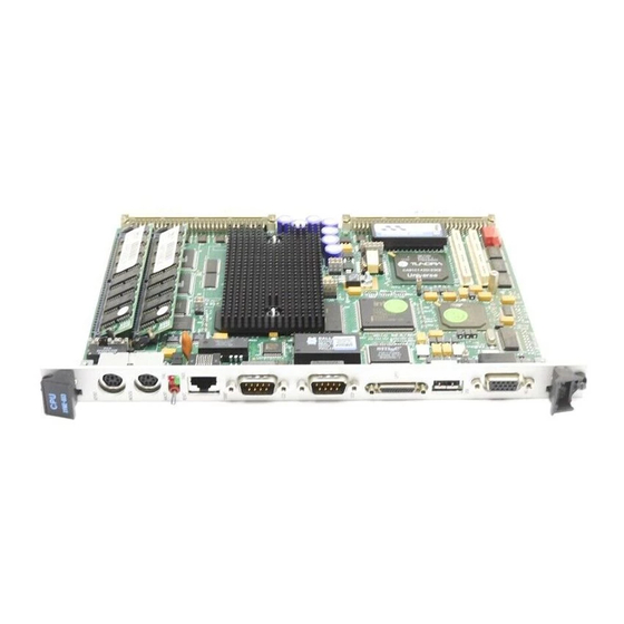
4. Verify that the card cage slot is clear and accessible. 5. Install the XVME-653/658 in the card cage by centering the unit on the plastic guides in the slots (P1 connector facing up). Push the board slowly toward the rear of the chassis until the P1 and P2 connectors engage. - Page 31 The floppy drive and hard drive are either cabled across P2 to the XVME-977 disk unit, or they are connected to the XVME-973/1 board. Refer to Chapter 5 for more information on the XVME-973/1. Figure 2-3 illustrates the XVME-653/658 front panel, to help you locate connectors. 2-15...
- Page 32 XVME-653/658 Manual Figure 2-3 XVME-653/658 Front Panel 2-16...
-
Page 33: Enabling The Pci Ethernet Controller
The DiskOnChip device is a self-contained solid-state disk drive that is packaged in a 32-pin device. It can be plugged into the onboard SRAM/Flash socket. Perform the following steps to configure the XVME-653/658 to use a DiskOnChip: 1. Plug the DiskOnChip into socket U9 on the CPU module. Be sure the direction is correct (pin 1 of the DiskOnChip is aligned with pin 1 of the socket). - Page 34 Windows NT onto the DiskOnChip (72 MB minimum), reduce the size of the Windows NT space requirement with a utility such as VenturCom Component Integra- tor™. If you use another operating system, please visit the M-Systems web site at www.m-sys.com or contact Xycom Automation Application Engineering at 734-429- 4971. 2-18...
-
Page 35: Chapter 3 - Bios Setup Menus
Chapter 3 – BIOS Setup Menus The XVME-653/658 customized BIOS is designed to surpass the functionality provided for normal PCs. This custom BIOS allows you to access the value-added features on the XVME-653/658 module without interfacing to the hardware directly. -
Page 36: Bios Main Setup Menu
XVME-653/658 Manual BIOS Main Setup Menu PhoenixBIOS Setup–Copyright 1985-95 Phoenix Technologies Ltd. Main Advanced Security VMEbus Exit Item Specific Help System Time: [16:19:20] System Date: [03/02/95] If the line item you are viewing Diskette A: [1.44 MB, 3½” ] has specific help, it will be listed &... - Page 37 – keys may be used to decrement them. It is not necessary to type zeros in front of numbers. Diskette A or B Selects the floppy disk drive installed in your system. The XVME-653/658 can only support one floppy drive (Drive A). Video System Selects the default video device.
-
Page 38: Ide Adapter 0 Master And Slave Submenus
XVME-653/658 Manual IDE Adapter 0 Master and Slave Submenus The IDE Adapter 0 Master and Slave submenus are used to configure IDE hard drive in- formation. If only one drive is attached to the IDE adapter, then only the parameters in the Master Submenu need to be entered. - Page 39 ENTER Type field to User and lets you edit the other fields. Do not attempt to manually set the disk drive parameters unless instructed to do so by Xycom Application Engineering. Type Options include 1 to 39, User, or Auto. The 1 to 39 option fills in all remaining fields with values for predefined disk type.
-
Page 40: Memory Cache Submenu
Enabling cache increases CPU performance by holding data most recently accessed in a special high-speed static RAM area called cache. The XVME-653/658 provides two lev- els of cache memory; level one is internal to the CPU (see CPU Chip on p. 1-2), and level two (external cache) is 512 KB of high-speed cache memory. -
Page 41: Memory Shadow Submenu
653/658 displays the number of KB allocated to Shadow RAM on the summary screen. The System Shadow field, which is not editable, is for reference only. The XVME-653/658 is shipped with both the system BIOS and video BIOS shadowed. PhoenixBIOS Setup–Copyright 1985-95 Phoenix Technologies Ltd. -
Page 42: Boot Sequence Submenu
XVME-653/658 Manual Boot Sequence Submenu This menu allows the boot sequence to be configured. PhoenixBIOS Setup–Copyright 1985-95 Phoenix Technologies Ltd. Main Boot Sequence Item Specific Help Previous Boot: [Disabled] Boot sequence: [A: then C:] If the line item you are viewing... -
Page 43: Numlock Submenu
Chapter 3 – BIOS Setup Menus Numlock Submenu PhoenixBIOS Setup–Copyright 1985-95 Phoenix Technologies Ltd. Main Keyboard Features Item Specific Help If the line item you are viewing Numlock: [Auto] has specific help, it will be listed Key Click: [Disabled] here. Keyboard auto-repeat rate: [30/sec] Keyboard auto-repeat delay:... -
Page 44: Advanced Menu
XVME-653/658 Manual Advanced Menu This menu allows you to change the peripheral control, advanced chipset control, and disk access mode. PhoenixBIOS Setup–Copyright 1985-95 Phoenix Technologies Ltd. Main Advanced Security VMEbus Exit Item Specific Help Warning! Setting items on this menu to incorrect values may cause your system to malfunction. -
Page 45: Integrated Peripherals Submenu
Chapter 3 – BIOS Setup Menus Integrated Peripherals Submenu The Integrated Peripherals Submenu is used to configure the COM ports and the parallel ports, and enable/disable the diskette, enhanced IDE controllers, and onboard BIOS. PhoenixBIOS Setup–Copyright 1985-95 Phoenix Technologies Ltd. Advanced Integrated Peripherals Item Specific Help... -
Page 46: 32-Pin Rom Site Submenu
XVME-653/658 Manual 32-Pin ROM Site Submenu The 32-Pin ROM Site Submenu lets you enable or disable this site, as well as specify the type of device that will occupy it if it is enabled. PhoenixBIOS Setup–Copyright 1985-95 Phoenix Technologies Ltd. -
Page 47: Advanced Chipset Control Submenu
Chapter 3 – BIOS Setup Menus Advanced Chipset Control Submenu Use this menu to change the values in the chipset registers and optimize your system’s performance. PhoenixBIOS Setup–Copyright 1985-95 Phoenix Technologies Ltd. Advanced Advanced Chipset Control Item Specific Help If the line item you are viewing DRAM Speed: [70ns] has specific help, it will be listed... -
Page 48: Security Menu
XVME-653/658 Manual Security Menu This menu prompts you for the new system password and requires you to verify the password by entering it again. The password can be used to stop access to the setup menus or prevent unauthorized booting of the unit. The supervisor password can also be used to change the user password. -
Page 49: Vmebus Setup Menu
Chapter 3 – BIOS Setup Menus VMEbus Setup Menu Using the VMEbus Setup menus, you are able to configure the XVME-653/658 VMEbus master and slave interfaces. This setup provides the following configurable items: • System Controller • Master Interface •... -
Page 50: System Controller Submenu
System resources are VMEbus Arbiter, BERR timeout, SYSCLK, and IACK daisy chain driver. These resources must be provided by the module installed in the sys- tem controller slot. The status of the XVME-653/658 system resources is reported in an uneditable field. -
Page 51: Master Interface Submenu
Chapter 3 – BIOS Setup Menus Master Interface Submenu The VMEbus master setup lets you configure the XVME processor board’s VMEbus master interface. Note When the master interface setting is turned on, master image 0 is re- served for BIOS use. To avoid conflict, master images 1, 2, and 3 are available for use. -
Page 52: Slave Interface Submenus
XVME-653/658 Manual Slave Interface Submenus The VMEbus slave setup allows configuration of the XVME processor board's VMEbus slave interfaces. Note When the Slave 1 & 2 Operational Mode setting is Compatible, slave images 0 and 1 are reserved for BIOS use. See p. 3-15 for more details. - Page 53 1 MB. Slave Base Address Sets the VMEbus address of the XVME-653/658 dual-access RAM. When the Slave Ad- dress Space option is set to VMEbus Standard (A24), the dual-access memory must be located on a 1 MB boundary and the upper two hex digits of the slave address are ig- nored.
-
Page 54: Exit Menu
XVME-653/658 Manual Exit Menu This menu prompts you to exit setup. PhoenixBIOS Setup–Copyright 1985-95 Phoenix Technologies Ltd. Main Advanced Security VMEbus Exit Item Specific Help Save Changes & Exit Exit Without Saving Changes If the line item you are viewing... -
Page 55: Bios Compatibility
Chapter 3 – BIOS Setup Menus Table 3-16 Exit Menu Options Option Description Save Changes & Exit After making your selections on the Setup menus, always select either Save Changes & Exit or Save Changes. Both procedures store the selections dis- played in the menus in battery-backed CMOS RAM. -
Page 57: Chapter 4 - Programming
Chapter 4 – Programming Memory Map Table 4-1 XVME-653/658 Memory Map Address Range Size Usage FFFC0000-FFFFFFFF 256 KB System BIOS Top of DRAM-FFFBFFFF Allocated to PCI bus by BIOS or operating system* 00100000-0FFFFFFF 256 MB System DRAM 00100000-07FFFFFF 128 MB... -
Page 58: I/O Map
XVME-653/658 Manual I/O Map Table 4-2 XVME-653/658 I/O Map Address Range Device 000-01F DMA controller 1, 8237A-5 equivalent 020-021 Interrupt controller 1, 8259 equivalent 022-023 Available 025-02F Interrupt controller 1, 8259 equivalent* 040-05F Timer, 8254-2 equivalent 060-06F Keyboard, 8742 equivalent... -
Page 59: Irq Map
The VME interface is the Tundra Universe chip, which is a PCI bus-to-VMEbus bridge device. The XVME-653/658 implements a 32-bit PCI bus and a 32/64-bit VMEbus inter- face. The Universe chip configuration registers are located in a 64 KB block of PCI memory space. -
Page 60: System Resources
VMEbus Master Interface The XVME-653/658 can act as a VMEbus master by accessing a PCI slave channel or by the DMA channel initiating a transaction. The Universe chip contains eight PCI slave images. Slave images 0 and 4 have a 4 KB resolution; the others (1-3, 5-7) have a 64 KB resolution. -
Page 61: Vmebus Interrupt Handling
VMEbus, causing the XVME-653/658 to become deadlocked. If the XVME-653/658 is to be used as a master and a slave at the same time, the VME- bus master cycles must obtain the VMEbus prior to initiating VMEbus cycles. -
Page 62: Vmebus Interrupt Generation
Consult the Universe User’s Manual for a more in-depth explanation. VMEbus Reset Options When the front panel Reset switch is toggled, the XVME-653/658 can perform the fol- lowing reset options: 1. Reset the VME backplane only. -
Page 63: Calling Conventions
Chapter 4 – Programming Calling Conventions The PCI BIOS functions preserve all registers and flags except those used for return pa- rameters. The Carry Flag [CF] will be altered as shown to indicate completion status. The calling routine will be returned to with the interrupt flag unmodified and interrupts will not be enabled during function execution. -
Page 64: Pci Bios Function Calls
XVME-653/658 Manual ENTRY: [EAX] Service Identifier = “$PCI” (049435024h) [EBX] Set to Zero EXIT: [AL] Return Code: 00h = SUCCESSFUL 80h = SERVICE_IDENTIFIER_NOT_FOUND 81h = INVALID VALUE IN [BL] [EBX] Physical address of the base of the PCI BIOS service [ECX] Length of the PCI BIOS service [EDX] Entry point into the PCI BIOS Service. -
Page 65: Read Configuration Byte
Chapter 4 – Programming Read Configuration Byte This function reads individual bytes from the configuration space of the VMEbus inter- face. ENTRY: [AH] BIOS_FUNCTION_ID = B1h [AL] BIOS_SUBFUNCTION_ID = 08h [BH] Bus Number (0-255) [BL] Device Number in upper 5 bits Function Number is bottom 3 bits [DI] Register Number (0...255) -
Page 66: Read Configuration Dword
XVME-653/658 Manual Read Configuration Dword This function reads individual dwords from the configuration space of the VMEbus in- terface. The Register Number parameter must be a multiple of four (i.e., bits 0 and 1 must be set to 0). ENTRY:... -
Page 67: Write Configuration Word
Chapter 4 – Programming Write Configuration Word This function writes individual words from the configuration space of the VMEbus inter- face. The Register Number parameter must be a multiple of two (i.e., bit 0 must be set to ENTRY: [AH] BIOS_FUNCTION_ID = B1h [AL] BIOS_SUBFUNCTION_ID = 0Ch... -
Page 68: Software-Selectable Byte-Swapping Hardware
Software-Selectable Byte-Swapping Hardware Software-selectable byte-swapping hardware is integrated into all XVME-658 and XVME-653/31x boards (see Table 1-1) to allow for the difference between the Intel and Motorola byte-ordering schemes, allowing easy communication over the VMEbus. The byte-swapping package incorporates several buffers either to pass data straight through or to swap the data bytes as they are passed through. - Page 69 Chapter 4 – Programming VMEbus Pentium Register (32 bit) Address XVME-653/658 VMEbus Figure 4-2 Address-Invariant Translation Notice that the internal data storage scheme for the PCI (Intel) bus is different from that of the VME (Motorola) bus. For example, the byte 78 (the least significant byte) is stored at location M on the PCI machine while the byte 78 is stored at the location M+3 on the VMEbus machine.
-
Page 70: Numeric Consistency
Universe chip to perform address-invariant byte-lane swapping. Numeric con- sistency is desirable for transferring integer data, floating-point data, pointers, etc. Con- sider the long word value 12345678h stored at address M by both the XVME-653/658 and the VMEbus, as shown in Figure 4-3. -
Page 71: Address Consistency
Address Consistency Address consistency, or address coherency, refers to communications between the XVME-653/658 and the VMEbus in which both architectures’ addresses are the same for each byte. In other words, the XVME-653/658 and the VMEbus memory images appear the same. Address consistency is desirable for byte-oriented data such as strings or video image data. -
Page 73: Chapter 5 - Xvme-973/1 Drive Adapter Module
The XVME-973/1 Drive Adapter Module is used to connect an external hard and floppy drive to your XVME-653/658 module. It has a single edge connector, labeled P2, that connects to the P2 backplane connector on the rear of the VME chassis. Figure 5-1 illus- trates how to connect the XVME-973/1 P2 connector to the VME chassis backplane P2 connector. -
Page 74: Connectors
XVME-653/658 Manual Connectors This section describes the pinouts for each of the five connectors on the XVME-973/1. P1 Connector The P1 connector connects up to two 3.5" hard drives. Power for the drives is not sup- plied by the XVME-973/1. -
Page 75: P2 Connector
Chapter 5 – XVME-973/1 Drive Adapter Module P2 Connector The XVME-973/1 P2 connector connects directly to the XVME-653/658 P2 connector through the VME chassis backplane. Table 5-2 XVME-973/1 P2 Connector Pinout HDRSTDRV* HD10 HD11 HD12 HD13 HD14 HD15 DIOW* FRWC*... -
Page 76: P3 Connector
XVME-653/658 Manual P3 Connector P3 connects a single 3.5" floppy drive. Only one drive is supported. Power for this drive is not supplied by the XVME-973/1. Table 5-3 XVME-973/1 P3 Connector Pinout Signal Signal FDIRC* FRWC* FSTEP* KEY (NC) FWD*... -
Page 77: P4 Connector
Chapter 5 – XVME-973/1 Drive Adapter Module P4 Connector P4 connects up to two 2.5" hard drives. Power for the drives is supplied by the connec- tor. Table 5-4 XVME-973/1 P4 Connector Pinout Signal Signal HDRSTDRV* DIOW* DIOR* IORDY HDACK* HD10 IRQ14 HD11... -
Page 78: P5 Connector
XVME-653/658 Manual P5 Connector P5 connects a single 3.5" floppy drive. Power for this drive is supplied by the connector. Table 5-5 XVME-973/1 P5 Connector Pinout Signal Signal FSTEP* IDX* FWD* FDS1* FWE* DCHG* FTKO* FWP* MO1* FRDD* FDIRC* FHS*... -
Page 79: Appendix A - Dram Installation
60 ns to run with the zero wait states. The XVME-653/658 supports 32, 64, 128, and 256 MB of DRAM. You can use 4Mx32, 8Mx32, 16Mx32 DRAM SIMM, and 32Mx32 DRAM SIMM sizes. Table A-1 lists the combinations needed for the memory configurations. - Page 80 XVME-653/658 Manual Insert DRAM module, angled at about 50° to the horizontal, as shown in top view A as shown in side view B Press DRAM module down until it snaps into place, as shown in side view C Figure A-1 DRAM Installation To remove a strip, pull outward on the plastic tab while lifting the end.
- Page 81 Table A-2 4M x 32 Part Numbers Manufacturer Part Number Samsung KMM5324004BSW-6 Viking Components VE432-416-60TS (fast page mode) Xycom Automation 104302 Table A-3 8M x 32 Part Numbers Manufacturer Part Number Samsung KMM5328004BSW-6 Viking Components VE832-416-60TS (fast page mode)
-
Page 83: Appendix B - Drawings
Appendix B – Drawings This appendix contains the board assembly drawings (top view) for the XVME-653/658. Figure B-1 is the assembly drawing for the XVME-658 and the XVME-653/31x mod- ules, both of which have the byte-swapping hardware. Figure B-2 is the assembly draw-... - Page 84 XVME-653/658 Manual C B A RN18 C B A C B A RN15 RN16 RN14 C B A 1 2 3 4 Figure B-1 Assembly Drawing for XVME-658 and XVME-653/31x...
- Page 85 Appendix B – Drawings C B A RN18 C B A C B A RN15 RN16 RN14 C B A 1 2 3 4 Figure B-2 Assembly Drawing for XVME-653/30x...
-
Page 87: Appendix C - Schematic
Appendix C – Schematic Appendix C – Schematic This appendix contains the schematic for the XVME-653/658. It consists of 22 pages and is for the XVME-658 and the XVME-653/31x, both of which have the byte-swapping hardware. To use the schematic with an XVME-653/30x module (which has no byte- swapping hardware), ignore the last page of the schematic (schematic page 22). - Page 111 Advanced Menu, BIOS setup....... 3-10 .............2-8 assembly drawing........B-2, B-3 VMEbus ..........2-10 auxiliary connector......... 2-9 interboard connector 1 (P4) .....2-12 backplane, installing the XVME-653 into ... 2-14 interboard connector 2 (P3) .....2-13 BIOS compatibility ........3-21 XVME-973/1 BIOS menus ..........5-2 Advanced Menu........3-10 ..........5-3...
- Page 112 PCI BIOS Flash BIOS ............. 1-4 16-bit interface .........4-7 floppy drive ............ 1-5 32-bit interface .........4-7 front panel, XVME-653/658 ......2-16 function calling conventions ....4-7 hard drive ..........1-5, 3-4 PCI BIOS functions ........4-6 hardware specifications........1-7 Locating the Universe Chip......4-8 humidity specifications ........
- Page 113 Index RJ-45 10/100 Base-T Connector:....2-17 video controller ..........1-2 Security Menu, BIOS setup......3-14 VME interface ..........4-3 serial port pinouts........... 2-7 VMEbus serial ports ..........1-4, 2-7 compliance..........1-7 shadow memory ..........3-7 interface............1-3 shock specifications ........1-7 interrrupt handling........4-5 specifications interrupt generation ........4-6 environmental ..........
Need help?
Do you have a question about the XVME-653 and is the answer not in the manual?
Questions and answers