
Subscribe to Our Youtube Channel
Related Manuals for Xycom XVME-100


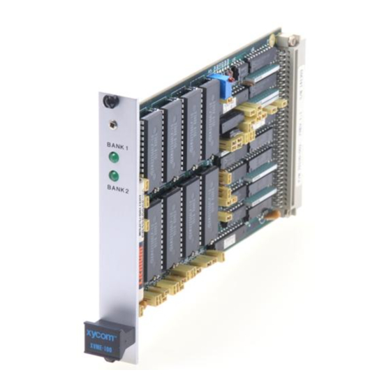
Summary of Contents for Xycom XVME-100
- Page 1 (217) 352-9330 | Click HERE Find the Acromag / Xembedded / Xycom XVME-100 at our website:...
- Page 2 • RAM/ROM MEMORY MODULE • © X Y C O M 1987 X Y C O M 750 N o r t h M a p l e R o a d Saline, M i c h i g a n 48176 Printed i n t h e U n i t e d States o f A m e r i c a (313) 429-4971 Part N u m b e r 74100-001...
- Page 3 This document contains proprietary information of Xycom Incorporated (Xycom). It shall not be reproduced or copied without expressed written authorization from Xycom. The information contained within this document is subject to change without notice. Xycom does not guarantee the accuracy of the information and makes no commitment toward keeping it up-to-date.
-
Page 4: Table Of Contents
X V M E - 1 0 0 M a n u a l March, 1987 • T A B L E O F C O N T E N T S C H A P T E R T I T L E PA G E M O D U L E D E S C R I P T I O N I n t r o d u c t i o n... - Page 5 X V M E - 1 0 0 M a n u a l March, 1987 • L I S T O F F I G U R E S F I G U R E T I T L E 1-I O p e r a t i o n a l B l o c k D i a g r a m 2-1 L o c a t i o n o f Jumpers, Sockets, a n d C o n n e c t o r 2 - l A E x p a n d e d L e f t Side o f X V M E - I 0 0...
-
Page 6: M O D U L E D E S C R I P T I O N
v M E - 1 0 0 M a n u a l \17r,.11, 1987 • Chapter 1 M O D U L E D E S C R I P T I O N 1.1 I N T R O D U C T I O N The X V M E - 1 0 0 R A M / R O M M e m o r y M o d u l e i s a s i n g l e - h i g h , V M E b u s c o m p a t i b l e board, w h i c h c a n a c c o m m o d a t e u p t o I M b y t e o f R A M , E P R O M , o r m a s k... -
Page 7: M O D U L E O P E R At I O N A L D E S C R I P T I O N
X V M E - 1 0 0 M a n u a l March, 1987 • 1.3 M O D U L E O P E R AT I O N A L D E S C R I P T I O N Figure 1 - I s h o w s a n d o p e r a t i o n a l b l o c k d i a g r a m o f t h e m e m o r y m o d u l e . -
Page 8: Specifications
XVME-100 Manual March, 1987 • 1.4 S P E C I F I C AT I O N S Table 1-1 lists the XVME-100 Memory Module's characteristics and specifications. Table 1-1. M e m o r y Module Specifications Specification Characteristic... - Page 9 X V M E - 1 0 0 M a n u a l March, 1987 • Ta b l e I - 1 . M e m o r y M o d u l e S p e c i f i c a t i o n s ( c o n t i n u e d ) C h a r a c t e r i s t i c E N V I R O N M E N T A L Te m p e r a t u r e...
-
Page 10: I N T R O D U C T I O N
X V M E - 1 0 0 M a n u a l March, 1987 • Chapter 2 X V M E - 1 0 0 I N S T A L L A T I O N 2.1 I N T R O D U C T I O N This c h a p t e r e x p l a i n s h o w t o c o n f i g u r e t h e m e m o r y m o d u l e p r i o r t o i n s t a l l a t i o n i n a V M E b u s system. - Page 11 X V M E - 1 0 0 M a n u a l March, 1987 • • C > J 4 2 J 4 8 1 J 4 9 J 5 0 J51 J 3 8 R N8 J 4 3 J 3 9 •...
- Page 12 X V M E - 1 0 0 M a n u a l March, 1987 • J12 1 J13 J 1 4 J15 J16 c— 0 1 / C . ) A B A B R N 5 • -•J A c_ J30 J31...
-
Page 13: Jumpers
X V M E - 1 0 0 M a n u a l March, 1987 • 2.3 J U M P E R S P r i o r t o i n s t a l l i n g t h e X V M E - 1 0 0 M e m o r y M o d u l e , i t w i l l b e necessary t o c o n f i g u r e several j u m p e r o p t i o n s . -
Page 14: Jumper D E S C R I P T I O N S
X V M E - 1 0 0 M a n u a l March, 1987 • Ta b l e 2-1. J u m p e r L i s t ( c o n t i n u e d ) Section Jumper Description... - Page 15 XVME-100 Manual March, 1987 • Table 2-2. V M E Base Address and Memory Chip Size Jumpers BANK 1 BASE ADDRESS B I T J14 I n * J14 Out J23 Out J23 I n * J21 I n *...
- Page 16 8E0000 Hex. through 8FFFFF Hex. Figure 2 - 2 shows t h e memory m a p f o r t h e XVME-100, a n d F i g u r e 2 - 3 shows t h e bank addressing f o u r times the memory chip size.
- Page 17 XVME-100 Manual March, 1987 WORD ADDRESS EVEN BYTES O D D BYTES BASE ADDRESS +4 X DEVICE SIZE - 2 BASE ADDRESS + 2 x DEVICE SIZE — BASE ADDRESS + 2 x DEVICE SIZE - 2 BASE ADDRESS BANK 1...
- Page 18 X V M E - 1 0 0 M a n u a l March, 1987 • ( 4 x DEVICE SIZE IN BYTES) BASE ADDRESS = n x ( 4 x DEVICE SIZE IN BYTES) BANK # 0 n = 0, 1, 2, 3, .. •...
- Page 19 X V M E - 1 0 0 M a n u a l March, 1987 • 2.4.2 A d d r e s s M o d i f i e r D e c o d e The a d d r e s s m o d i f i e r d e c o d e u s e s t h r e e j u m p e r s f o r e a c h b a n k ( 6 t o t a l ) . B o t h banks r e s i d e i n t h e s t a n d a r d A 2 4 address space.
-
Page 20: M E M O R Y Device Speed
XVME-100 Manual March, 1987 These t h r e e jumpers a r c independent o f each o t h e r. W h e n b o t h t h e d a t a space select and t h e program space select jumpers arc out, the bank w i l l be disabled f r o m VMEbus accesses. -
Page 21: M E M O R Y Device P I N O U T
X V M E - 1 0 0 M a n u a l March, 1987 • 2.4.4 M e m o r y Device P i n o u t T h c r c a r c s e v e n j u m p e r s f o r e a c h o f t h e b a n k s ( 1 4 t o t a l ) o n t h e X V M E - 1 0 0 w h i c h d e f i n e t h e m e m o r y d e v i c e p i n o u t . - Page 22 X V M E - 1 0 0 M a n u a l March, 1987 • MASI{ P R O G R A M M A B L E R O M A t , NC C . 7 U - 2 7 : 7 Vcc (*56) NC E 1 1 "...
- Page 23 X V M E - 1 0 0 M a n u a l March, 1987 • E X A M P L E : Bank 1 8 K x 8 R A M M e m o r y d e v i c e p i n o u t j u m p e r s Memory Ty p e J 4 5 J 4 3 J 4 6 J 4 1 J 4 2 J 4 0 J 4 4 64k B i t s O U T @...
-
Page 24: M E M O R Y Backup Power
XVME-100 Manual March, 1987 • 2.4.5 M e m o r y Backup Power During p o w e r loss, t h e CMOS R A M chips m a y h a v e a n alternative p o w e r source connected t o r e t a i n t h e d a t a stored. - Page 25 XVME-100 Manual March, 1987 • To calculate the typical battery l i f e , use the following equation: Hours o f battery l i f e = 1 , 4 0 0 , 0 0 0 ((n x IsB) + 10)
- Page 26 XVME-100 Manual March, 1987 • The user has three d i f f e r e n t options available f o r choosing alternate power source of each bank. T h e s e options depend o n t h e configurations o f J34 a n d J35 a n d arc...
-
Page 27: Power M O N I T O R
X V M E - 1 0 0 M a n u a l March, 1987 • 2.4.6 P o w e r M o n i t o r A p o w e r m o n i t o r i s p r o v i d e d t o disable t h e m e m o r y c h i p s w h e n V c c f a l l s b e l o w 4.75V. -
Page 28: I N S T A L L I N G M E M O R Y C H I P S O N T H E X V M
X V M E - 1 0 0 M a n u a l March, 1987 • POT R 3 P O I N T S R3 7 3 • J12 J13 I J14 -J15 - - - . 7 . 6 * - - N . - Page 29 March, 1987 2.5 I N S T A L L I N G MEMORY CHIPS ON T H E XVME-100 As was previously mentioned, there arc a total o f t i g h t 32-pin sockets intended f o r use b y R A M , E P R O M , EEPROM, a n d M a s k Programmable R O M dcviccs o n t h e XVME-100 Module.
-
Page 30: Cardcage I N S T A L L A T I O N P R O C E D U R E
X V M E - 1 0 0 M a n u a l March, 1987 • 4) C h e c k t o m a k e s u r e t h a t t h e c h i p s a r e f u l l y seated i n t h e b o t t o m o f t h e sockets, w i t h n o p i n s b e n t o r o u t o f a l i g n m e n t i n t h e sockets. -
Page 31: I N S T A L L I N G A 6U Front Panel K I T (Optional)
2.7 I N S T A L L I N G A 6U FRONT PANEL K I T (optional) XYCOM Model N u m b e r XVME-945 i s a n optional 6 U f r o n t panel k i t designed t o replace t h e e x i s t i n g 3 U f r o n t p a n e l o n t h e X V M E - I 0 0 . - Page 32 X V M E - 1 0 0 M a n u a l March, 1987 • • • Figure 2-8. I n s t a l l a t i o n o f a n X V M E - 9 4 5 6 U F r o n t P a n c l 2-23...
- Page 33 • • •...
- Page 34 • Appendix A VMEbus CONNECTOR/PIN DESCRIPTION Table A - I . P 1 - VMEbus Signal Identification Connector Signal Mnemonic Pin Number Signal Name and Description AC F A I L U R E : O p e n -collectors d r i v e n s i g n a l w h i c h ACFAIL* 1B:3 indicates t h a t t h e A C i n p u t t o t h e power supply i s n o...
- Page 35 XVME-100 Manual March, 1987 • Table A-1. V M E b u s Signal Identification (cont'd) Connector Signal Mnemonic Pin Number Signal Name and Description A0I-A23 I A:24-30 ADDRESS B U S ( b i t s 1-23): Thrcc-state d r i v e n address 1C:15-30 lines that specify a memory address.
- Page 36 X V M E - 1 0 0 M a n u a l March, 1987 • Ta b l e A - 1 . V M E b u s S i g n a l I d e n t i f i c a t i o n ( c o n t ' d ) Connector Signal Mnemonic...
- Page 37 X V M E - 1 0 0 M a n u a l March, 1987 • Ta b l e A - 1 . V M E b u s Signal I d e n t i f i c a t i o n ( c o n t ' d ) Connector Signal Mnemonic...
- Page 38 X V M E - 1 0 0 M a n u a l March, 1987 • Ta b l e A - I . V M E b u s Signal I d e n t i f i c a t i o n ( c o n t ' d ) Connector Signal Mnemonic...
- Page 39 X V M E - 1 0 0 M a n u a l March, 1987 • B A C K P L A N E C O N N E C T O R P1 The f o l l o w i n g t a b l e l i s t s t h e P 1 p i n a s s i g n m e n t s b y p i n n u m b e r o r d e r . ( T h e connector consists o f t h r e e r o w s o f p i n s labeled r o w s A , B , a n d C.) Ta b l e A - 2 .
- Page 40 X V M E - I 0 0 M a n u a l March, 1987 A p p e n d i x B • POWER M O N I T O R A p o w e r m o n i t o r i s p r o v i d e d t o d i s a b l e t h e m e m o r y c h i p s w h e n V C C f a l l s b e l o w 4.75V.
-
Page 41: L O C A T I O N O F Jumpers A N D Te S T P O I N T S
X V M E - 1 0 0 M a n u a l March, 1987 • POT R 3 P O I N T S • (3:1\ \ - 1 J 2 0 B A B R N 5 Figure B-1. - Page 42 X V M E - 1 0 0 M a n u a l March, 1987 • A p p c n d i x C D I A G R A M A N D S C H E M AT I C S 0 33 a, co —...
- Page 43 XVME-100 Manual March, 1987 • • Operational Block Diagram •...
- Page 44 XVME-100 Manual March, 1987 • VMEBUS ADDRESS DECODE 7 4 F 3 7 3 AM5 ( P I C 1 4 5 0 1 2 11 0 A 2 3 F L I C - 1 5 ) 70 1 6...
- Page 46 ALL CAPACITORS ARE I N MICROFARAOS. I 1 0 K ALL DESCRETE RESISTORS ARE I N OHMS 1/411.5%. 2 . B Y PA S S CAPS ARE . 1 u F O50V.AND ARE DESIGNATED A S C B P. XVME-100 Schematic Sheet 1 of 4...
- Page 48 X V M E - 1 0 0 M a n u a l March, 1987 • - 0 . + 5 V 1 10K 7 4 9 L 5 2 4 5 - 1 ( P I A I ( P 1 A - - 2 BOO , 8 0 0...
- Page 49 R e v. A K I > B 0 0 - 8 0 1 5 3 . 4 7 - 1 V H I O K H ( P I P — 1 6 O TA C K . 0 0 0 M R . 3 .
- Page 50 XVME-100 Manual March, 1987 • 2 8 0 0 - B 0 1 5 B 9 1 - 8 9 1 7 V BU- 4 11 - 0 3 4 4 • B A 1 4, 8 9 1 B 9 2 B 9 3 •...
- Page 51 ...,, BA9 ‘ 7 Al) ..BA10 BA10 .._BAlt 23 A 1 0 Al 0 ,,,,BBA01 123 BA12 25 A l l A l l BA13 A l 2 A l 2 B1917 .XVME-100 Schematic, Sheet 3 o f 4...
- Page 52 XVN1E-100 M a n u a l \ l a r c h , 1987 • 2 B 0 0 - 8 0 1 5 B P 1 - B 8 1 7 \ D - V BU + 5 V - 01 3 2 12 A O BD I...
- Page 53 MEMORY B A N K 2 301 3 2 B D 0 • B A 1 3 1 ) 0 8 3 B 0 8 14 B 0 9 4 B D 9 4 B D 1 • B A 2 B C 1 5 B D 1 0 _ , 15 E I D L „...
- Page 54 XVME-100 Manual March, 1987 • Appendix D QUICK REFERENCE G U I D E Table D-1. J u m p e r List Section Jumper Description Power Monitor Calibration 2.4.6 Memory Type - bank 2 2.4.4 Memory Type - bank 2 2.4.4...
- Page 55 XVME-100 Manual March, 1987 Table D-1. J u m p e r List (continued) Jumper Description Section Memory Type - bank 1 2.4.4 Memory Type - bank 1 2.4.4 Memory Type - bank 1 2.4.4 Memory Type - bank 1 2.4.4...
- Page 56 XVME-100 Manual March, 1987 • Table D-2. V M E Base Address and Memory Chip Size Jumpers BANK 1 BASE ADDRESS B I T J14 Out J14 I n * J23 Out J23 I n * J21 O u t...
- Page 57 XVME-100 Manual March, 1987 • Table D-3. Address Modifier Jumpers BANK 1 Jumpers Description Supervisor Only A M 2 = 1 J13 I n * Supervisor & Non-privileged A M 2 = don't care J13 Out Data Access R e s p o n d s to Address Modifier...
- Page 58 XVME-100 Manual March, 1987 • Table D-4. M e m o r y Device Speed Jumpers BANK 1 Jumpers Speed Select J6 J 7 100ns 150ns 200ns 250ns BANK 2 Jumpers Speed Select J4 J 5 100ns 150ns 200ns 250ns •...
- Page 59 XVME-100 Manual March, 1987 • Alternate Powcr Source = Battery (J34B, J35 O U T ) Bank 1 Power J 4 4 Battery Vcc* Bank 2 Powcr Battery Vcc* Alternate Power Source = +5V Standby (J34A, J35 I N )
Need help?
Do you have a question about the XVME-100 and is the answer not in the manual?
Questions and answers