Table of Contents
Advertisement
UM2036
User manual
Evaluation board with STM32F779NI MCU
Introduction
The STM32F779I-EVAL evaluation board is a complete demonstration and development
®
®
platform for STMicroelectronics ARM
Cortex
-M7 core-based STM32F779NI
2
microcontrollers. It features the following interfaces: four I
Cs, six SPIs with three
2
multiplexed full-duplex I
S, SDIO, two SAIs, 8-bit to 14-bit digital camera, Ethernet MAC,
FMC, Quad-SPI. It also features four USARTs and four UART peripherals, two CAN buses,
three 12-bit ADC converters, two 12-bit DAC channels, internal 512 Kbytes of SRAM + 16
Kbytes of instruction, 2 Mbytes of Flash memory, TCM RAM + 4 Kbytes of backup SRAM,
USB OTG HS and USB OTG FS peripherals, SWD and JTAG debugging support,
Cryptographic acceleration (hardware acceleration for AES 128, 192, 256, triple DES,
HASH (MD5, SHA-1, SHA-2), and HMAC). This evaluation board can be used as a
reference design for user application development but it is not considered as a final
application.
The full range of hardware features on the board helps the user to evaluate all the
™
peripherals (USB OTG HS, USB OTG FS, Ethernet, motor control, microSD
card, USART,
audio DAC and ADC, digital microphone, CAN, SRAM, NOR Flash, SDRAM, Quad SPI
Flash, 4" DSI LCD with capacitive touch panel etc.) and develop applications. Extension
headers make provide an easy mean of connecting a daughterboard for a specific
application.The integrated ST-LINK/V2-1 provides an embedded in-circuit debugger and
programmer for the STM32.
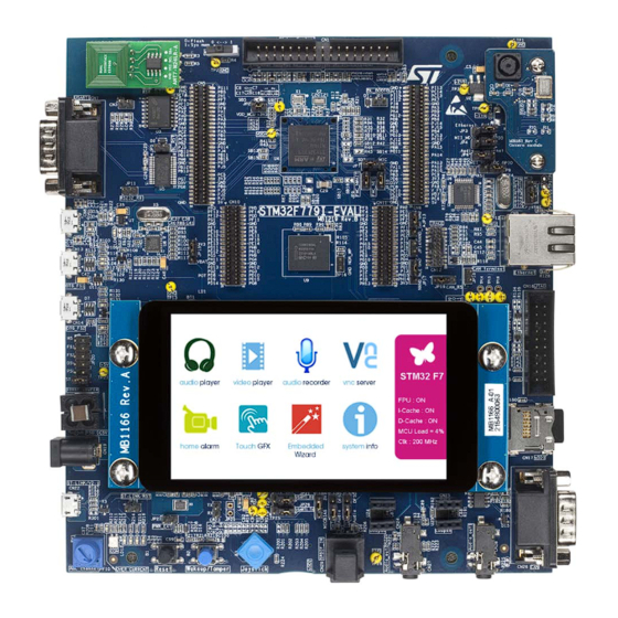
Figure 1. STM32F779I-EVAL evaluation board
1. Picture is not contractual.
March 2017
DocID029088 Rev 3
1/80
www.st.com
1
Advertisement
Table of Contents

Subscribe to Our Youtube Channel
Related Manuals for ST STM32F779I-EVAL


Summary of Contents for ST STM32F779I-EVAL
-
Page 1: User Manual
UM2036 User manual Evaluation board with STM32F779NI MCU Introduction The STM32F779I-EVAL evaluation board is a complete demonstration and development ® ® platform for STMicroelectronics ARM Cortex -M7 core-based STM32F779NI microcontrollers. It features the following interfaces: four I Cs, six SPIs with three... -
Page 2: Table Of Contents
Embedded ST-LINK/V2-1 ........12... - Page 3 SPDIF IN connector CN29 ........49 Appendix A STM32F779I-EVAL I/O assignment......50 Appendix B Schematics .
- Page 4 Contents UM2036 IC Compliance Statement ........77 C.2.1 Compliance Statement .
- Page 5 STM32F779I-EVAL I/O assignment ........
- Page 6 STM32F779I-EVAL evaluation board layout ........11...
-
Page 7: Features
• I C Extension interface • RS-232 connector • JTAG/SWD and ETM trace debug support, ST-LINK/V2-1 embedded • IEEE-802.3-2002 compliant Ethernet connector • Camera module • 8Mx32bit SDRAM, 1Mx16bit SRAM and 8Mx16bit NOR Flash • 512-Mbit Quad-SPI NOR Flash ®... -
Page 8: Demonstration Software
Any consequences deriving from such usage will not be at ST charge. In no event, ST will be liable for any customer usage of these engineering sample tools as reference design or in production. -
Page 9: Delivery Recommendations
UM2036 Delivery recommendations Delivery recommendations Before using the board for the first time, the user should check that it has not been visibly damaged during the shipment, and that no components are unplugged or missing. When the board is extracted from its plastic bag, check that no component remains in the bag. The main components to verify are: 25 MHz crystal (X4) which may have been removed by a shock from its socket. -
Page 10: Hardware Layout And Configuration
UM2036 Hardware layout and configuration Hardware layout and configuration STM32F779I-EVAL evaluation board is designed around the STM32F779NI (216-pin in TFBGA package). The hardware block diagram Figure 2 illustrates the connection between STM32F779NI and peripherals (SDRAM, SRAM, NOR Flash, Quad-SPI Flash, Camera... -
Page 11: Figure 3. Stm32F779I-Eval Evaluation Board Layout
UM2036 Hardware layout and configuration Figure 3. STM32F779I-EVAL evaluation board layout CN10, CN11 Camera extension Memory connector Motor control connector connector CN5, CN6 Extension CN12 Ethernet OTG2 HS CN15 DSI LCD CN13 OTG1 FS CN14 OTG2 FS CN16 JTAG CN17... -
Page 12: Embedded St-Link/V2-1
172.72mm 37.7mm 20.18mm 20.18mm Embedded ST-LINK/V2-1 The ST-LINK/V2-1 programming and debugging tool is integrated on the STM32F779I- EVAL evaluation board. Compared to ST-LINK/V2 the changes are listed below. The new features supported on the ST-LINK/V2-1 are: • USB software re-enumeration •... -
Page 13: Drivers
ETM signals. In this way SAI, Ethernet and camera are not functional and NOR Flash and SRAM addresses are limited to A18. Note: 2 When JP28 is open, the NRST of the ST-LINK MCU (U21) is pulled high. When JP28 is closed, ST-LINK MCU is reset. 6.1.1... -
Page 14: Power Supply
Hardware layout and configuration Power supply The STM32F779I-EVAL evaluation board is designed to be powered by the 5 V DC power supply and to be protected from wrong power plug-in event by PolyZen. It is possible to configure the evaluation board to use any of the following power supply six sources: •... -
Page 15: Table 2. Power-Supply-Related Jumper Settings
JP15 is set, as shown to the right: JP20 is used to select one of the six possible power supply resources. STM32F779I-EVAL is supplied through the jack CN19, when JP20 is set as shown to the right: (Default Setting) - Page 16 STM32F779I-EVAL is supplied from the USB OTG1 FS (CN13), when JP20 is set as shown on the right: JP20 STM32F779I-EVAL is supplied from the USB OTG2 HS (CN8) when JP20 is set as shown to the right: STM32F779I-EVAL is supplied from power supply jack (CN19) and daughterboard connected on CN5 and CN6, when JP20 is set as shown on the right (daughterboard must not have its own power supply connected).
-
Page 17: Clock Source
UM2036 Hardware layout and configuration The LED LD10 is lit when the STM32F779I-EVAL evaluation board is powered by the 5 V correctly. To avoid the impact of USB PHY and Ethernet PHY and get precise results of current consumption on JP2, the following cautions must be taken into account:... -
Page 18: Reset Source
UM2036 Hardware layout and configuration Reset source The reset signal of the STM32F779I-EVAL evaluation board is active low and the reset sources include: • Reset button B1 • Debugging tools from JTAG/SWD connector CN16 and ETM trace connector CN12 •... -
Page 19: Audio
CN28. External speakers can be connected to WM8994ECS/R via the audio jack CN27. Two digital microphones (MEMS microphone) MP34DT01TR are available on the STM32F779I-EVAL evaluation board. They can be connected to either the audio codec or the DFSDM port of the STM32F779NI by setting jumpers shown in Table 7: Audio related jumpers. - Page 20 UM2036 Hardware layout and configuration Table 7. Audio related jumpers (continued) Jumper Description PD6 is as SD2_CLK signal when JP7 is set as shown to the right (Default setting): PD6 is connected to DFSDM_DATA1 when JP7 is set as shown to the right (Also need to set JP23 together according to this table): Digital microphone power source is connected to +3.3V power when JP22 is set as shown to the right (Default setting):...
-
Page 21: Usb Otg1 Fs
Green LED LD5 (for CN8) or LD9 (for CN14) is lit when either power switch (U7) is ON and the STM32F779I-EVAL works as a USB host or VBUS is powered by another USB host, when the STM32F779I-EVAL works as a USB device. -
Page 22: Microsd Cards
UM2036 Hardware layout and configuration Note: The STM32F779I-EVAL board should be powered by external power supply when using OTG function. RS-232 RS-232 communication is supported by D-type 9-pins RS-232 connector CN7, which is connected to the USART1 of the STM32F779NI on the STM32F779I-EVAL evaluation board. -
Page 23: Can
MII serial management signals (MDIO and MDC) are simulated by GPIOs (PJ12 and PJ13) by default on the STM32F779I-EVAL. The original MII serial management signals of the Ethernet IP in the STM32F779NI can be also used by setting JP3 and JP6. Refer... -
Page 24: Memories
UM2036 Hardware layout and configuration Table 11. Ethernet related jumpers Jumper Description 25MHz clock is provided by external crystal X4 when JP12 is set as shown to the right: (Default setting) JP12 25MHz clock for MII is provided by MCO at PA8 when JP12 is set as shown to the right: MDIO connect to MII_MDIO_GPIO when JP4 is set as shown to the right: (Default setting) -
Page 25: Quad-Spi Nor Flash
In such cases, memory addresses A19 to A22 not connected to FMC are pulled down, so that memories can be addressed within a limited address range. If A21 or A22 is required, the camera board should be removed from the STM32F779I-EVAL board. 6.14... -
Page 26: Camera Module
UM2036 Hardware layout and configuration 6.16 Camera module A connector CN4 for DCMI signals is on STM32F779I-EVAL evaluation board and camera module daughterboard MB1183. DCMI signals are duplicated with other peripherals (SAI, I S, NOR Flash, microSD cards, trace and MEMS microphone). These peripherals may not function correctly if camera module is being used. -
Page 27: Motor Control
DSI_RESET 6.18 Motor control The STM32F779I-EVAL evaluation board supports both asynchronous and synchronous three-phase brushless motor control via a 34-pin connector CN1, which provides all required control and feedback signals to and from the motor-power-driving board. Available signals on this connector include emergency stop, motor speed, 3-phase motor current, bus voltage, heatsink temperature coming from the motor driving board and six channels of PWM control signal going to the motor driving circuit. -
Page 28: Figure 6. Stm32F779I-Eval Evaluation Board Motor Control Pcb Reworks (Top Side)
UM2036 Hardware layout and configuration Figure 6. STM32F779I-EVAL evaluation board motor control PCB reworks (Top side) Motor Control Flash 0 <--> 1 Sys mem I2C_EXT Camera +2V8 PI11 PI13 +3V3 BL_BOOT0 PC15 PC14 RESET# PI15 PC13 USART1 PI12 VREF+ PF10... -
Page 29: Table 15. Motor Control Related Solder Bridges
UM2036 Hardware layout and configuration Figure 7. STM32F779I-EVAL evaluation board motor control PCB reworks (Bottom side) C101 C102 R226 R228 R229 SB34 R233 SB35 SB36 R236 SB37 R237 SB42 R238 C103 SB43 SB44 C104 R240 C106 C107 R239 C108 SB45... -
Page 30: Multi-Function Expander
6.19 Multi-Function expander The Multi-Function expander (MFX) is implemented as an I/O expander circuit on the STM32F779I-EVAL evaluation board. The communication interface between MFX and STM32F779NI is done through the I2C1 interface. The signals connected to MFX are listed in Table 16: MFX signals Table 16. -
Page 31: Connectors
UM2036 Connectors Connectors Motor control connector CN1 Figure 8. Motor control connector CN1 (Top view) Table 17. Motor control connector CN1 Pin of Pin of Description number number Description STM32F779NI STM32F779NI of CN1 of CN1 Emergency STOP MC_UH MC_UL MC_VH MC_VL MC_WH MC_WL... -
Page 32: I 2 C Connector Cn2
UM2036 Connectors C connector CN2 Figure 9. I C connector CN2 (Front view) Table 18. I C connector CN2 Pin number Description Pin number Description I2C1_SDA (PB9) +3V3 I2C1_SCL (PB8) RESET (PC10) Analog input-output connector CN3 Figure 10. Analog input-output connector CN3 (Top view) Table 19. -
Page 33: Camera Module Connector Cn4
UM2036 Connectors Camera module connector CN4 Figure 11. Camera module connector CN4 (Top view) Table 20. Camera module connector CN4 Pin number Description Pin number Description +1.8V +1.8V D0 (PC6) D1 (PC7) D10 (PD6) D2 (PC8) D11 (PD2) D3 (PC9) D4 (PC11) D5 (PD3) D8 (PC10) -
Page 34: Daughterboard Extension Connectors Cn5 And Cn6
Two 60-pin male headers CN5 and CN6 can be used to connect a daughterboard or the standard wrapping board to the STM32F779I-EVAL evaluation board. All GPIOs are dispatched on memory connectors (CN10 and CN11), and on connectors CN5 and CN6. - Page 35 UM2036 Connectors Table 21. Daughterboard extension connector CN5 (continued) How to disconnect with function block on Description Alternative function STM32F779I-EVAL board LCD_R7/FMC_NE3 Open SB20 PJ10 PI11 ULPI_DIR Remove R122 ULPI_D7/LCD_G7 Remove R117, open SB5 OSC_OUT Remove R20, close SB41 QSPI_BK1_IO2...
-
Page 36: Table 22. Daughterboard Extension Connector Cn6
UM2036 Connectors Table 21. Daughterboard extension connector CN5 (continued) How to disconnect with function block on Description Alternative function STM32F779I-EVAL board LCD_R3/DSI_TE Disconnect CN15 LCD_R2/LED2 Open SB15 +5 V Table 22. Daughterboard extension connector CN6 How to disconnect with function block on... - Page 37 UM2036 Connectors Table 22. Daughterboard extension connector CN6 (continued) How to disconnect with function block on Description Alternative Function STM32F779I-EVAL board Open SB17 SB72,SB75, disconnect CN4 and SD1_D0/MC_WH/PAR_D2 Remove R282, disconnect CN4, disconnect PC11 SD1_D3 /PAR_D4 PC10 SD1_D2/EXT_RESET/PAR_D8 Remove R287,R16, disconnect CN4 and SD1...
-
Page 38: Rs-232 Connector Cn7
UM2036 Connectors Table 22. Daughterboard extension connector CN6 (continued) How to disconnect with function block on Description Alternative Function STM32F779I-EVAL board SD2_CMD Disconnect SD2 MC_UH/PAR_D0/I2S3_CK Open SB18, disconnect CN4, keep JP9 on open +5 V RS-232 connector CN7 Figure 12. RS-232 connector CN7 (Front view) Table 23. -
Page 39: Ethernet Rj45 Connector Cn9
UM2036 Connectors Table 24. USB OTG HS Micro-AB connector CN8 Pin number Description Pin number Description VBUS Ethernet RJ45 connector CN9 Figure 14. Ethernet RJ45 connector CN9 (Front view) Table 25. RJ45 connector CN9 Pin number Description Description number TxData+ TxData- RxData+ Shield... -
Page 40: Table 26. Memory Connector Cn10
UM2036 Connectors Table 26. Memory connector CN10 How to disconnect with function block on Description Function STM32F779I-EVAL board SDNE0/MII_COL Open SB57 PF13 PF12 PE10 PE12 PE15 PE13 PD11 PD12 A15/BA1 PH11 PD13 PD14 SDNWE PF14 PF11 SDNRAS PE11 PF15 PE14... -
Page 41: Table 27. Memory Connector Cn11
UM2036 Connectors Table 26. Memory connector CN10 (continued) How to disconnect with function block on Description Function STM32F779I-EVAL board PH12 PD10 PD15 SDCLK/ MII_PPS_OUT Table 27. Memory connector CN11 How to disconnect with function block on Description Alternative function STM32F779I-EVAL board... -
Page 42: Etm Trace Debugging Connector Cn12
UM2036 Connectors Table 27. Memory connector CN11 (continued) How to disconnect with function block on Description Alternative function STM32F779I-EVAL board NWAIT /MC_UH/ PAR_D0 Close JP9, disconnect CN4 and CN1 A23/TRACECLK/ MII_TXD3 Open SB10, remove R42 NE1/MC_VH/ PAR_D0 Connect JP10, disconnect CN4,CN1... -
Page 43: Usb Otg1 Fs Micro-Ab Connector Cn13
UM2036 Connectors Table 28. ETM trace debugging connector CN12 Pin number Description Description number +3.3V TMS/PA13 TCK/PA14 TDO/PB3 TDI/PA15 RESET# TraceCLK/PE2 TraceD0/PE3 or SWO/PB3 TraceD1/PE4 or nTRST/PB4 TraceD2/PE5 TraceD3/PE6 7.11 USB OTG1 FS Micro-AB connector CN13 Figure 16. USB OTG1 FS Micro-AB connector CN13 (Front view) Table 29. -
Page 44: Usb Otg2 Fs Micro-Ab Connector Cn14
UM2036 Connectors 7.12 USB OTG2 FS Micro-AB connector CN14 Figure 17. USB OTG2 FS Micro-AB connector CN14 (Front view) Table 30. USB OTG2 FS Micro-AB connector CN14 Pin number Description Pin number Description VBUS (PB13) ID (PB12) D- (PB14) D+ (PB15) 7.13 JTAG/SWD connector CN16 Figure 18. -
Page 45: Microsd Connectors Cn17 And Cn30
UM2036 Connectors Table 31. JTAG/SWD debugging connector CN16 (continued) Pin number Description Description number RTCK RESET# DBGRQ DBGACK 7.14 microSD connectors CN17 and CN30 Figure 19. microSD connector (Top view) Table 32. microSD card1 connector CN17 Description Description number number SDMMC_D2 (PC10) Vss/GND SDMMC_D3 (PC11) -
Page 46: Power Connector Cn19
MicroSDcard_detect2 (MFX SDMMC_CLK( PD6) GPIO10) 7.15 Power connector CN19 STM32F779I-EVAL evaluation board can be powered from a DC 5V power supply via the external power supply jack (CN19) shown in Figure 20. The central pin of CN19 must be positive. -
Page 47: Mems Microphone Coupon Connectors Cn24 And Cn25
UM2036 Connectors Figure 21. USB Micro-B connector (Front view) Table 34. USB Micro-B connector CN22 Pin number Description Pin number Description VBUS (power) 6,7,8,9,10,11 Shield 7.19 MEMS microphone coupon connectors CN24 and CN25 Figure 22. MEMS microphone coupon connectors CN24 and CN25 (Top view) Table 35. -
Page 48: Can D-Type 9-Pin Male Connector Cn26
CANL 3,5,6 7.21 Audio jack (speaker) CN27 A 3.5mm stereo audio jack CN27 for speaker out is available on the STM32F779I-EVAL evaluation board to support external speaker. 7.22 Audio jack CN28 A 3.5mm stereo audio jack CN28 is available on the STM32F779I-EVAL evaluation board to support headset (headphone and microphone integrated). -
Page 49: Spdif In Connector Cn29
UM2036 Connectors 7.23 SPDIF IN connector CN29 Figure 24. SPDIF IN connector CN29 (Front view) Table 37. SPDIF IN connector CN29 Pin number Description Pin number Description SPDIF_RX1(PG12) DocID029088 Rev 3 49/80... -
Page 50: Appendix A Stm32F779I-Eval I/O Assignment
UM2036 STM32F779I-EVAL I/O assignment Appendix A STM32F779I-EVAL I/O assignment Table 38. STM32F779I-EVAL I/O assignment STM32F779I-EVAL Camera Pin No. Pin Name Motor control variant standard variant A20/TRACED1 A19/TRACED0 A23/TRACECLK/MII_TXD3 PG14 MII_TXD1 NBL1 NBL0 Audio and EXPANDER and ACP and RF_I2C1_SCL ULPI_D7/LCD_G7... - Page 51 UM2036 STM32F779I-EVAL I/O assignment Table 38. STM32F779I-EVAL I/O assignment (continued) STM32F779I-EVAL Camera Pin No. Pin Name Motor control variant standard variant VBAT VBAT PI8- ANTI EXPANDER_INT TAMP2 NBL2 LCD_DE/DSI_RESET LCD_B7 LCD_B6 PG12 SPDIF_RX1 PG10 SD2_D1 PJ14 LCD_B2 DFSDM_CLK PA11 CAN1_RX/USB_FS1_DM...
- Page 52 UM2036 STM32F779I-EVAL I/O assignment Table 38. STM32F779I-EVAL I/O assignment (continued) STM32F779I-EVAL Camera Pin No. Pin Name Motor control variant standard variant PI12 LCD_HSYNC PDR_ON BOOT BOOT VDD_3 VDD_11 VDD_10 VDD_15 VCAP2 PH13 PH14 RS232_USART1_TX/ USB_FS1_VBUS PC15- OSC32_OUT OSC32_OUT VSS_18 VSS_13...
- Page 53 UM2036 STM32F779I-EVAL I/O assignment Table 38. STM32F779I-EVAL I/O assignment (continued) STM32F779I-EVAL Camera Pin No. Pin Name Motor control variant standard variant PI13 LCD_VSYNC PI15 LCD_R0/LED0 VDD_18 VSS_17 VSS_9 VDDUSB PJ11 SD1_D0/NAND_NCE WH_TIM8_CH3 FMC_NE1 VH_TIM8_CH2 PH1 - OSC_OUT OSC_OUT PI14 LCD_CLK...
- Page 54 UM2036 STM32F779I-EVAL I/O assignment Table 38. STM32F779I-EVAL I/O assignment (continued) STM32F779I-EVAL Camera Pin No. Pin Name Motor control variant standard variant NAND_INT FMC_NE3 QSPI_BK1_IO2 QSPI_BK1_IO3 SDCKE0 VDD_4 VSS_4 VSS_6 VSS_7 VSS_1 VSS_14 VDD_14 PD15 PB13 ULPI_D6/USB_FS2_VBUS PD10 PF10 POT_ADC3_IN8 QSPI_BK1_IO1...
- Page 55 UM2036 STM32F779I-EVAL I/O assignment Table 38. STM32F779I-EVAL I/O assignment (continued) STM32F779I-EVAL Camera Pin No. Pin Name Motor control variant standard variant ULPI_STP SAI1_SD_A/MII_MDC CURRENT_A_ADC1_123_IN11 MII_TXD2 CURRENT_B_ADC2_123_IN12 QSPI_CLK PF12 PF15 LCD_R5 PD12 PD13 LCD_R6 PH12 VREF- MII_RX_CLK ENCODER_B_TIM5_5_CH2 PA0-WKUP SAI2_SD_B/MII_CRS ENCODER_A_TIM5_5_CH1...
- Page 56 UM2036 STM32F779I-EVAL I/O assignment Table 38. STM32F779I-EVAL I/O assignment (continued) STM32F779I-EVAL Camera Pin No. Pin Name Motor control variant standard variant PF14 LCD_R3/DSI_TE PF11 SDNRAS PE11 PE14 PB10 ULPI_D3 DISSIPATIVE_BRAKE_TIM2_12_C MII_RXD2 PH10 VDDA ULPI_D0 MII_RX_DV UL_TIM8_CH1N ULPI_D2 WL_TIM8_CH3N ULPI_D1 VL_TIM8_CH2N...
-
Page 57: Appendix B Schematics
UM2036 Schematics Appendix B Schematics This section provides design schematics for the STM32F779I-EVAL key features to help users to implement these features in application designs. This section includes: • Overall schematics for the board, see Figure 25 • MCU connections, see Figure 26 •... -
Page 58: Figure 25. Stm32F779I-Eval Evaluation Board
Figure 25. STM32F779I-EVAL evaluation board U_MCU MCU.SchDoc U_Memory R160 Same length Memory.SchDoc +3V3 I2C1_SCL R161 I2C1_SDA A[0..23] A[0..23] U_Audio D[0..31] D[0..31] Audio.SchDoc 90MHz clock SDCLK SDCLK I2C1_SCL SAI2_SCKB SAI2_SCKB SDNE0 SDNE0 I2C1_SDA SAI2_FSB SAI2_FSB SDNRAS SDNRAS SAI2_SDB SAI2_SDB SDNCAS SDNCAS... -
Page 59: Figure 26. Stm32F779I-Eval Mcu
Figure 26. STM32F779I-EVAL MCU SB45 Open MC_EnA Wakeup Button SB47 Open MII_CRS SB43 Closed SAI2_SDB ULPI_STP SB34 Open Open SB42 +3V3 MC_EnB MC_CurrentA SB36 Closed MII_RX_CLK R219 SB37 Open MC_EnIndex MII_MDC Closed SB44 MII_MDIO SAI1_SDA SB35 Closed Open SB49 SAI2_SCKB... -
Page 60: Figure 27. Stm32F779I-Eval Power
Figure 27. STM32F779I-EVAL Power ZEN056V130A24LS CN19 220uF DC-10B SMAJ5.0A-TR 100nF BNX002-01 +3V3 VDD_MCU JP20 VBUS_HS VBUS_FS1 TP21 TP13 TP26 +3V3 LD1117S18TR +1V8 VBUS_FS2 LD10 Ground Ground Ground Ground Vout R140 U5V_ST_LINK 11 12 10uF Header 6X2 +3V3 LD1117STR +2V8 LD1086D2M33... -
Page 61: Figure 28. Stm32F779I-Eval Sram, Flash, Sdram
Figure 28. STM32F779I-EVAL SRAM, FLASH, SDRAM D[0..31] D[0..31] A[0..23] A[0..23] DQ31 DQ30 I/O15 DQ15A-1 DQ29 I/O14 DQ14 DQ28 I/O13 DQ13 DQ27 I/O12 DQ12 DQ26 I/O11 DQ11 DQ25 I/O10 DQ10 DQ24 I/O9 DQ23 I/O8 DQ22 I/O7 DQ21 I/O6 DQ20 I/O5 DQ19... -
Page 62: Figure 29. Stm32F779I-Eval Audio
Figure 29. STM32F779I-EVAL Audio +3V3 LDO1VDD AGND Default I2C Address:0011010 +3V3 AVDD1 AGND SPKVDD1 AGND +1V8 SPKVDD2 SPKGND1 AVDD2 SPKGND2 +1V8 CPVDD CPGND +3V3 DCVDD DGND DBVDD HP2GND +1V8 LDO2VDD R174 I2C1_SDA R170 R175 +3V3 LDO1ENA SCLK I2C1_SCL R173[N/A] LDO2ENA... -
Page 63: Figure 30. Stm32F779I-Eval Lcd, Camera, Connector
Figure 30. STM32F779I-EVAL LCD, camera, connector RGB LCD Camera PAR_D[0..11] PAR_D[0..11] CN18 LCD_R[0..7] PI15 LCD_R0 LCD_G0 LCD_G[0..7] C102 +1V8 C101 LCD_R[0..7] LCD_G[0..7] LCD_R1 LCD_G1 LCD_R2 LCD_G2 100nF 100nF LCD_R3 LCD_G3 LCD_R4 LCD_G4 PB10 +3V3 +1V8 11 12 LCD_R5 LCD_G5 PB11... -
Page 64: Figure 31. Stm32F779I-Eval Ethernet
Figure 31. STM32F779I-EVAL Ethernet +3V3 R128 100nF R118 R112 100nF MII_TX_CLK TX_CLK PG11 MII_TX_EN TX_EN PG13 MII_TXD0 TXD_0 PG14 MII_TXD1 TXD_1 MII_TXD2 TXD_2 MII_TXD3 TXD_3/SNI_MODE MII_RXD0 RXD_0/PHYAD1 MII_RXD1 RXD_1/PHYAD2 LED(green)_A MII_RXD2 RXD_2/PHYAD3 LED(green)_K MII_RXD3 RXD_3/PHYAD4 LED(Yellow)_A PI10 MII_RX_ER RX_ER/MDIX_EN LED(Yellow)_K... -
Page 65: Figure 32. Stm32F779I-Eval Usb Otg Hs
Figure 32. STM32F779I-EVAL USB OTG HS +3V3 R133 CN14 PB13 VBUS_FS2 VBUS PB14 D1_N USB_FS2_DM PB15 D1_P USB_FS2_DP PB12 USB_FS2_ID Green Shield Shield R136 ESDA6V1BC6 Shield 9013 Shield 475900001 R137 +3V3 R119 MFX_GPIO8 OTG_FS2_OverCurrent SB22 +3V3 To MFX R120 MFX_GPIO9... -
Page 66: Figure 33. Stm32F779I-Eval Usb Otg Fs
Figure 33. STM32F779I-EVAL USB OTG FS +3V3 R127 MFX_GPIO6 OTG_FS1_OverCurrent R131 To MFX R132 CN13 FAULT VBUS MFX_GPIO7 R130 D2_N OTG_FS1_PowerSwitchOn D2_P From MFX STMPS2151STR 4.7uF R129 Shield Shield Shield Shield 475900001 +3V3 VBUS_FS1 PA11 USB_FS1_DM PA12 USB_FS1_DP PA10 R115... -
Page 67: Figure 34. Stm32F779I-Eval Rs-232
Figure 34. STM32F779I-EVAL RS-232 +3V3 ST3241EBPR C132 C133 100nF 100nF DB9-male USART1 C131 100nF 100nF 100nF T1IN T1OUT RS232_TX T2IN T2OUT T3IN T3OUT R1OUTB Bootloader_BOOT0 R2OUTB R1OUT R1IN JP11 R2OUT R2IN PA10 RS232_RX R3OUT R3IN Bootloader_RESET R4OUT R4IN R5OUT R5IN... -
Page 68: Figure 35. Stm32F779I-Eval Can And Quad-Spi
Figure 35. STM32F779I-EVAL CAN and Quad-SPI +3V3 R183 R189 +3V3 CN26 C179 Default setting: 1<->2 DB9-male CAN connector Default setting: Open JP19 100nF PA12 JP18 CAN1_TX CANH CANL PA11 CAN1_RX Vref R185 SN65HVD230 ESDCAN24-2BLY R184 R186 Optional [N/A] +3V3 Quad SPI Flash... -
Page 69: Figure 36. Stm32F779I-Eval Peripherals
Figure 36. STM32F779I-EVAL Peripherals +3V3 MICRO SD1 (TF) Card R158 R154 R153 R157 R156 Potentiometer +3V3 SD1_D1 two pin header for external analog input +3V3 SD1_D0 PC11 SD1_D3 PC10 SD1_D2 PC12 SD1_CLK SD1_CMD PF10 Potentiometer 100nF R29 0 3386P-103(10K) [N/A]... -
Page 70: Figure 37. Stm32F779I-Eval Motor Control
Figure 37. STM32F779I-EVAL motor control +3V3 Motor control connector MC_EmergencySTOP EMERGENCY STOP [N/A] MC_UH MC-UH MC_UL MC_UL MC_VH MC_VH MC_VL MC_VL MC_WH MC_WH MC_WL MC_WL BUS VOLTAGE MC_BusVoltage MC_CurrentA CURRENT A CURRENT B 100nF 100K CURRENT C [N/A] PG11 MC_NTC... -
Page 71: Figure 38. Stm32F779I-Eval Extension Connectors
Figure 38. STM32F779I-EVAL extension connectors Place close Memory SB40 Left Right CN10 Open PI11 PI13 SDNE0 SDNWE SB39 SB38 SB41 PC15 PC14 PF13 PF14 R226 Open PI15 PC13 Open PF12 RESET# Open PI12 PF11 SDNRAS PF10 11 12 11 12... -
Page 72: Figure 39. Stm32F779I-Eval St-Link/V2-1
Figure 39. STM32F779I-EVAL ST-LINK/V2-1 VBUS_HS +3V3_ST_LINK BAT60JFILM R208 R207 VBUS_FS1 BAT60JFILM BAT60JFILM U14 LD3985M33R +3V3_ST_LINK C169 C171 C176 C174 JP27 VBUS_FS2 Vout 100nF 100nF 100nF 100nF +3V3_ST_LINK BAT60JFILM BYPASS R168 1uF_X5R_0603 1uF_X5R_0603 BAT60JFILM 100K +3V3_ST_LINK 100nF 10nF_X7R_0603 100nF BAT60JFILM Board Ident: PC13=0... -
Page 73: Figure 40. Stm32F779I-Eval Mfx And Leds
Figure 40. STM32F779I-EVAL MFX and LEDs +3V3 Green PI15 R216 LED0 Orange R215 LED1 Multi Function eXpander +3V3 +3V3 +3V3 one capacitor close to each MFX pins: VDD, VDD_1, VDD_2, VDD_3 R214 LED2 Ferrite C173 C178 C172 C170 C175 Blue... -
Page 74: Figure 41. Stm32F779I-Eval Jtag And Trace
Figure 41. STM32F779I-EVAL JTAG and trace +3V3 R139 R141 R134 R135 [N/A] [N/A] [N/A] [N/A] PA13 TMS/SWDIO PA14 TCK/SWCLK TDO/SWO PA15 R110 TRST R102 RESET# R138 [N/A] Trace connector JTAG connector CN16 CN12 +3V3 JTAG +3V3 +3V3 R142 [N/A] R143... -
Page 75: Figure 42. Stm32F779I-Eval 4-Inch Dsi Lcd Board
Figure 42. STM32F779I-EVAL 4-inch DSI LCD board BLGND HSSI_CLK_N HSSI_CLK_N HSSI_CLK_P HSSI_CLK_P HSSI_CLK_P HSSI_CLK_N HSSI_D0_N HSSI_D0_N HSSI_D0_P HSSI_D0_P HSSI_D0_P HSSI_D0_N HSSI_D1_N HSSI_D1_N HSSI_D1_P HSSI_D1_P HSSI_D1_P BLVDD HSSI_D1_N BLVDD RESX BEAD CABC CABC 4.7uH(1A) BLGND 4.7uF/50V Open LEDA BLVDD LEDK STPS1L40M... -
Page 76: Figure 43. Stm32F779I-Eval Camera Module
Figure 43. STM32F779I-EVAL camera module +1V8 100nF 100nF +2V8 11 12 13 14 15 16 Camera_RST 17 18 STANDBY EXTCLK 19 20 +2V8 +2V8 +2V8 21 22 Camera_CLK PAR_D0 PAR_D1 MCLK AVDD(2.8V) 23 24 PAR_PCLK [N/A] PAR_D2 PAR_D3 PCLK DVDD(1.8V) -
Page 77: Appendix C Federal Communications Commission (Fcc) And Industry Canada (Ic) Compliance Statements
UM2036 Federal Communications Commission (FCC) and Industry Canada (IC) Compliance Appendix C Federal Communications Commission (FCC) and Industry Canada (IC) Compliance Statements FCC Compliance Statement C.1.1 Part 15.19 This device complies with Part 15 of the FCC Rules. Operation is subject to the following two conditions: (1) this device may not cause harmful interference, and (2) this device must accept any interference received, including interference that may cause undesired operation. -
Page 78: Appendix Dcispr32
UM2036 CISPR32 Appendix D CISPR32 Warning Warning: This device is compliant with Class A of CISPR32. In a residential environment, this equipment may cause radio interference. 78/80 DocID029088 Rev 3... -
Page 79: Revision History
UM2036 Revision history Revision history Table 39. Document revision history Date Revision Changes 23-May-2016 Initial release. Added sections: Section Appendix C: Federal Communications 02-Dec-2016 Commission (FCC) and Industry Canada (IC) Compliance Statements, Section Appendix D: CISPR32. Added boot loader note in Section 6.5: Boot option 08-Mar-2017 ESD protection note in... - Page 80 ST products and/or to this document at any time without notice. Purchasers should obtain the latest relevant information on ST products before placing orders. ST products are sold pursuant to ST’s terms and conditions of sale in place at the time of order acknowledgement.
Need help?
Do you have a question about the STM32F779I-EVAL and is the answer not in the manual?
Questions and answers