Table of Contents
Advertisement
Quick Links
Advertisement
Table of Contents

Related Manuals for Alinx AXU4EV-E


Summary of Contents for Alinx AXU4EV-E
- Page 1 ZYNQ UltraScale+ FPGA Development Board AXU4EV-E User Manual...
-
Page 2: Version Record
ZYNQ Ultrascale + FPGA Board AXU4EV-E User Manual Version Record Version Date Release By Description Rev 1.0 2021-04-12 Rachel Zhou First Release Amazon Store: https://www.amazon.com/alinx 2 / 58... -
Page 3: Table Of Contents
ZYNQ Ultrascale + FPGA Board AXU4EV-E User Manual Table of Contents Version Record.......................2 Part 1: FPGA Development Board Introduction..........6 Part 2: ACU4EV core board................10 Part 2.1: ACU4EV core board Introduction..........10 Part 2.2: ZYNQ Chip................... 11 Part 2.3: DDR4 DRAM................13 Part 2.4: QSPI Flash...................20... - Page 4 ZYNQ Ultrascale + FPGA Board AXU4EV-E User Manual Part 3.14: EEPROM and Temperature sensor........53 Part 3.15: User LEDs..................54 Part 3.16: Keys.................... 55 Part 3.17: DIP Switch Configuration............55 Part 3.18: Power Supply................56 Part 3.19: ALINX Customized Fan............57 Part 3.20: Carrier Board Size Dimension..........58 Amazon Store: https://www.amazon.com/alinx...
- Page 5 ZYNQ Ultrascale + FPGA Board AXU4EV-E User Manual This MPSoCs FPGA development platform adopts the core board + carrier board mode, which is convenient for users to use the core board for secondary development. The core board uses XILINX Zynq UltraScale+ EV chip ZU4EV...
-
Page 6: Part 1: Fpga Development Board Introduction
256Mb QSPI FLASH which are on the PS side, used to statically store the operating system, file system and user data of MPSoCs. The AXU4EV-E carrier board expands its rich peripheral interface, including 1 SATA M.2 interface, 1 DP interface, 4 USB 3.0 Interface, 2 Gigabit... - Page 7 ZYNQ Ultrascale + FPGA Board AXU4EV-E User Manual Figure 1-1-1: The Schematic Diagram of the AXU4EV-E Through this diagram, you can see the interfaces and functions that the AXU4EV-E FPGA Development Board contains: ACU4EV core board It consists of ZU4EV +4GB DDR4 (PS) +1GB DDR4 (PL) +8GB eMMC FLASH + 256Mb QSPI FLASH, and there are 2 crystal oscillators to provide the clock, a single-ended 33.3333MHz crystal oscillator for the...
- Page 8 ZYNQ Ultrascale + FPGA Board AXU4EV-E User Manual display. Supports up to 4K@30Hz or 1080P@60Hz output USB 3.0 Interface 4-channel USB3.0 HOST interface, USB interface type is TYPE A. Used to connect external USB peripherals, such as connecting a mouse, keyboard, U disk, etc.
- Page 9 ZYNQ Ultrascale + FPGA Board AXU4EV-E User Manual MIPI camera input interfaces, used to connect MIPI camera module (AN5641). JTAG debug port A 10-pin 0.1 spacing standard JTAG ports for FPGA program download and debugging. Users can debug and download the ZU4EV system through the XILINX downloader.
-
Page 10: Part 2: Acu4Ev Core Board
ZYNQ Ultrascale + FPGA Board AXU4EV-E User Manual Part 2: ACU4EV core board Part 2.1: ACU4EV core board Introduction ACU4EV (core board model, the same below) FPGA core board, ZYNQ chip is based on XCZU4EV-1SFVC784I of XILINX company Zynq UltraScale+ MPSoCs EV Family. -
Page 11: Part 2.2: Zynq Chip
ZYNQ Ultrascale + FPGA Board AXU4EV-E User Manual Figure 2-1-1: ACU4EV Core Board (Front View) Part 2.2: ZYNQ Chip The FPGA core board ACU4EV uses Xilinx's Zynq UltraScale+ MPSoCs EV family chip, module XCZU4EV-1SFVC784I. The PS system of the ZU4EV chip integrates 4 ARM Cortex™-A53 processors with a speed of up to 1.2Ghz... - Page 12 ZYNQ Ultrascale + FPGA Board AXU4EV-E User Manual Figure 2-2-1: Overall Block Diagram of the ZYNQ ZU4EV Chip The main parameters of the PS system part are as follows: ARM quad-core Cortex ™ -A53 processor, speed up to 1.5GHz, each...
-
Page 13: Part 2.3: Ddr4 Dram
ZYNQ Ultrascale + FPGA Board AXU4EV-E User Manual Sata 3.1, Display Port, 4 x Tri-mode Gigabit Ethernet Common connection interfaces: 2 x USB2.0, 2 x SD/SDIO, 2 x UART, 2 x CAN 2.0B, 2 x I2C, 2 x SPI, 4 x 32b GPIO ... - Page 14 ZYNQ Ultrascale + FPGA Board AXU4EV-E User Manual of 1GB. The maximum operating speed of the DDR4 SDRAM on the PS side can reach 1200MHz (data rate 2400Mbps), and the 4 DDR4 storage systems are directly connected to the memory interface of the PS BANK504. The...
- Page 15 ZYNQ Ultrascale + FPGA Board AXU4EV-E User Manual The hardware connection of DDR4 SDRAM on the Pl Side is shown in Figure 2-3-2: Figure 2-3-2: DDR3 DRAM schematic diagram PS Side DDR4 DRAM pin assignment: Signal Name Pin Name Pin Number...
- Page 16 ZYNQ Ultrascale + FPGA Board AXU4EV-E User Manual PS_DDR4_DQS6_N PS_DDR_DQS_N6_504 PS_DDR4_DQS7_P PS_DDR_DQS_P7_504 PS_DDR4_DQS7_N PS_DDR_DQS_N7_504 PS_DDR4_DQ0 PS_DDR_DQ0_504 AD21 PS_DDR4_DQ1 PS_DDR_DQ1_504 AE20 PS_DDR4_DQ2 PS_DDR_DQ2_504 AD20 PS_DDR4_DQ3 PS_DDR_DQ3_504 AF20 PS_DDR4_DQ4 PS_DDR_DQ4_504 AH21 PS_DDR4_DQ5 PS_DDR_DQ5_504 AH20 PS_DDR4_DQ6 PS_DDR_DQ6_504 AH19 PS_DDR4_DQ7 PS_DDR_DQ7_504 AG19 PS_DDR4_DQ8 PS_DDR_DQ8_504...
- Page 17 ZYNQ Ultrascale + FPGA Board AXU4EV-E User Manual PS_DDR4_DQ31 PS_DDR_DQ31_504 AC28 PS_DDR4_DQ32 PS_DDR_DQ32_504 PS_DDR4_DQ33 PS_DDR_DQ33_504 PS_DDR4_DQ34 PS_DDR_DQ34_504 PS_DDR4_DQ35 PS_DDR_DQ35_504 PS_DDR4_DQ36 PS_DDR_DQ36_504 PS_DDR4_DQ37 PS_DDR_DQ37_504 PS_DDR4_DQ38 PS_DDR_DQ38_504 PS_DDR4_DQ39 PS_DDR_DQ39_504 PS_DDR4_DQ40 PS_DDR_DQ40_504 PS_DDR4_DQ41 PS_DDR_DQ41_504 PS_DDR4_DQ42 PS_DDR_DQ42_504 PS_DDR4_DQ43 PS_DDR_DQ43_504 PS_DDR4_DQ44 PS_DDR_DQ44_504 PS_DDR4_DQ45 PS_DDR_DQ45_504 PS_DDR4_DQ46...
- Page 18 ZYNQ Ultrascale + FPGA Board AXU4EV-E User Manual PS_DDR4_DM1 PS_DDR_DM1_504 AE23 PS_DDR4_DM2 PS_DDR_DM2_504 AE25 PS_DDR4_DM3 PS_DDR_DM3_504 AE28 PS_DDR4_DM4 PS_DDR_DM4_504 PS_DDR4_DM5 PS_DDR_DM5_504 PS_DDR4_DM6 PS_DDR_DM6_504 PS_DDR4_DM7 PS_DDR_DM7_504 PS_DDR4_A0 PS_DDR_A0_504 PS_DDR4_A1 PS_DDR_A1_504 PS_DDR4_A2 PS_DDR_A2_504 AB28 PS_DDR4_A3 PS_DDR_A3_504 AA28 PS_DDR4_A4 PS_DDR_A4_504 PS_DDR4_A5 PS_DDR_A5_504 AA27...
- Page 19 ZYNQ Ultrascale + FPGA Board AXU4EV-E User Manual PS_DDR4_CLK0_N PS_DDR_CK0_N_504 PS_DDR4_CKE0 PS_DDR_CKE0_504 PL Side DDR4 DRAM pin assignment: Signal Name Pin Name Pin Number PL_DDR4_DQS0_P IO_L22P_T3U_N6_DBC_AD0P_64 PL_DDR4_DQS0_N IO_L22N_T3U_N7_DBC_AD0N_64 PL_DDR4_DQS1_P IO_L16P_T2U_N6_QBC_AD3P_64 PL_DDR4_DQS1_N IO_L16N_T2U_N7_QBC_AD3N_64 PL_DDR4_DQ0 IO_L24N_T3U_N11_64 PL_DDR4_DQ1 IO_L24P_T3U_N10_64 PL_DDR4_DQ2 IO_L23N_T3U_N9_64 PL_DDR4_DQ3 IO_L23P_T3U_N8_64...
-
Page 20: Part 2.4: Qspi Flash
ZYNQ Ultrascale + FPGA Board AXU4EV-E User Manual PL_DDR4_A7 IO_L2P_T0L_N2_64 PL_DDR4_A8 IO_L9P_T1L_N4_AD12P_64 PL_DDR4_A9 IO_L1P_T0L_N0_DBC_64 PL_DDR4_A10 IO_L4N_T0U_N7_DBC_AD7N_64 PL_DDR4_A11 IO_L7N_T1L_N1_QBC_AD13N_64 PL_DDR4_A12 IO_L6N_T0U_N11_AD6N_64 PL_DDR4_A13 IO_L1N_T0L_N1_DBC_64 PL_DDR4_BA0 IO_T1U_N12_64 PL_DDR4_BA1 IO_L5N_T0U_N9_AD14N_64 PL_DDR4_RAS_B IO_T2U_N12_64 PL_DDR4_CAS_B IO_L5P_T0U_N8_AD14P_64 PL_DDR4_WE_B IO_L11N_T1U_N9_GC_64 PL_DDR4_ACT_B IO_L13N_T2L_N1_GC_QBC_64 PL_DDR4_CS_B IO_L6P_T0U_N10_AD6P_64 PL_DDR4_BG0 IO_L2N_T0L_N3_64 PL_DDR4_RST IO_L7P_T1L_N0_QBC_AD13P_64... -
Page 21: Part 2.5: Emmc Flash
ZYNQ Ultrascale + FPGA Board AXU4EV-E User Manual QSPI FLASH is connected to the GPIO port of the BANK500 in the PS section of the ZYNQ chip. In the system design, the GPIO port functions of these PS ports need to be configured as the QSPI FLASH interface. Figure 2-4-1 shows the QSPI Flash in the schematic. - Page 22 ZYNQ Ultrascale + FPGA Board AXU4EV-E User Manual related parameters of eMMC FLASH are shown in Table 2-5-1. Position Model Capacity Factory MTFC8GAKAJCN-4M 8G Byte Micron Table 2-5-1: eMMC FLASH Specification The eMMC FLASH is connected to the GPIO port of the BANK500 of the PS part of the ZYNQ UltraScale+.
-
Page 23: Part 2.6: Clock Configuration
ZYNQ Ultrascale + FPGA Board AXU4EV-E User Manual MMC_DAT7 PS_MIO20_500 AD19 MMC_CMD PS_MIO21_500 AC21 MMC_CCLK PS_MIO22_500 AB20 MMC_RSTN PS_MIO23_500 AB18 Part 2.6: Clock configuration The core board provides reference clock and RTC real-time clock for PS system and PL logic respectively, so that PS system and PL logic can work independently. - Page 24 ZYNQ Ultrascale + FPGA Board AXU4EV-E User Manual Figure 2-6-2: Passive Crystal Oscillator for RTC Clock pin assignment: Signal Name PS_PADI_503 PS_PADO_503 PS System Clock Source The X1 crystal on the core board provides a 33.333MHz clock input for the PS part.
-
Page 25: Part 2.7: Led
ZYNQ Ultrascale + FPGA Board AXU4EV-E User Manual PL System Clock Source The core board provides a differential 200MHz PL system clock source for the reference clock of the DDR4 controller. The crystal oscillator output is connected to the global clock (MRCC) of PL BANK64. This global clock can be used to drive the DDR4 controller and user logic circuits in the FPGA. -
Page 26: Part 2.8: Power Supply
ZYNQ Ultrascale + FPGA Board AXU4EV-E User Manual Figure 2-7-1: LED Schematic in the Core Board Part 2.8: Power Supply The power supply voltage of the ACU4EV core board is DC12V, which is supplied by connecting the carrier board. The core board uses a PMIC chip TPS6508641 to generate all the power required by the XCZU4EV chip. - Page 27 ZYNQ Ultrascale + FPGA Board AXU4EV-E User Manual In addition, the VCCIO power supply of BANK65 and BANK66 of XCZU4EV chip is provided by the carrier board, which is convenient for users to modify, but the maximum power supply cannot exceed 1.8V.
-
Page 28: Part 2.9: Acu4Ev Core Board Size Dimension
ZYNQ Ultrascale + FPGA Board AXU4EV-E User Manual Part 2.9: ACU4EV Core Board Size Dimension Figure 2-9-1: ACU4EV Core Board Size Dimension Part 2.10: Board to Board Connectors pin assignment The core board has a total of four high-speed expansion ports. It uses four 120-pin inter-board connectors (J29/J30/J31/J32) to connect to the carrier board. - Page 29 ZYNQ Ultrascale + FPGA Board AXU4EV-E User Manual the level standard of MIO is also 1.8V. Pin assignment of board to board connector J29 J29 Pin Signal Name Pin Number J29 Pin Signal Name Pin Number B65_L2_N B65_L22_P B65_L2_P B65_L22_N...
- Page 30 ZYNQ Ultrascale + FPGA Board AXU4EV-E User Manual B66_L3_N B65_L12_N B66_L1_P B65_L13_N B66_L1_N B65_L13_P B66_L6_P B65_L21_P B66_L6_N B65_L21_N B66_L16_P B65_L23_P B66_L16_N B65_L23_N B66_L15_P B66_L5_N B66_L15_N B66_L5_P B66_L4_P B66_L2_P B66_L4_N B66_L2_N B66_L11_P B66_L20_P B66_L11_N B66_L20_N B66_L12_P B66_L7_P B66_L12_N B66_L7_N B66_L13_N B66_L10_P...
- Page 31 ZYNQ Ultrascale + FPGA Board AXU4EV-E User Manual B66_L22_P FPGA_TDO B66_L22_N FPGA_TMS B66_L19_N B66_L21_N B66_L19_P B66_L21_P B66_L24_P B66_L17_P B66_L24_N B66_L17_N B66_L23_N B25_L9_P B66_L23_P B25_L9_N B25_L5_N B25_L10_P B25_L5_P B25_L10_N B66_L18_N B25_L12_P B66_L18_P B25_L12_N B25_L4_N B25_L11_P B25_L4_P B25_L11_N B26_L11_P B25_L6_N B26_L11_N B25_L6_P...
- Page 32 ZYNQ Ultrascale + FPGA Board AXU4EV-E User Manual B26_L1_P B26_L12_P B26_L1_N B26_L12_N 505_CLK2_P 505_CLK1_P 505_CLK2_P 505_CLK1_P 505_CLK0_P 505_CLK3_P 505_CLK0_N 505_CLK3_N 505_TX3_P 505_TX1_P 505_TX3_N 505_TX1_N 505_RX3_P 505_TX0_P 505_RX3_N 505_TX0_N 505_TX2_P 505_RX1_P 505_TX2_N 505_RX1_N 505_RX2_P 505_RX0_P 505_RX2_N 505_RX0_N Pin assignment of board to board connector J31...
- Page 33 ZYNQ Ultrascale + FPGA Board AXU4EV-E User Manual B24_L12_P B24_L2_P AG14 B24_L12_N AA12 B24_L2_N AH14 B24_L3_P AG13 B24_L3_N AH13 B44_L12_N B44_L9_P AA11 B44_L12_P AB10 B44_L9_N AA10 B44_L10_N B44_L3_P AH12 B44_L10_P B44_L3_N AH11 B24_L11_N B44_L1_N AH10 B24_L11_P B44_L1_P AG10 B24_L9_N B24_L4_P...
- Page 34 ZYNQ Ultrascale + FPGA Board AXU4EV-E User Manual 224_RX3_P 224_TX3_P 224_RX3_N 224_TX3_N 224_RX2_P 224_TX2_P 224_RX2_N 224_TX2_N 224_RX1_P 224_TX1_P 224_RX1_N 224_TX1_N 224_RX0_P 224_TX0_P 224_RX0_N 224_TX0_N Pin assignment of board to board connector J32 J32 Pin Signal Name Pin Number J32 Pin...
- Page 35 ZYNQ Ultrascale + FPGA Board AXU4EV-E User Manual PS_MIO61 PS_MIO39 PS_MIO62 PS_MIO38 PS_MIO63 PS_MIO65 PS_MIO40 PS_MIO66 PS_MIO44 PS_MIO67 PS_MIO45 PS_MIO68 PS_MIO47 PS_MIO64 PS_MIO48 PS_MIO69 PS_MIO41 PS_MIO74 PS_MIO32 PS_MIO73 PS_MIO46 PS_MIO72 PS_MIO50 PS_MIO71 PS_MIO49 PS_MIO75 PS_MIO34 PS_MIO70 PS_MIO26 PS_MIO43 PS_MIO24 AB19...
- Page 36 ZYNQ Ultrascale + FPGA Board AXU4EV-E User Manual +12V +12V +12V +12V +12V +12V +12V +12V +12V +12V Amazon Store: https://www.amazon.com/alinx 36 / 58...
-
Page 37: Part 3: Carrier Board
ZYNQ Ultrascale + FPGA Board AXU4EV-E User Manual Part 3: Carrier Board Part 3.1: Carrier Board Introduction Through the previous function introduction, you can understand the function of the carrier board part 1-Channel M.2 interface 1-Channel DP output interface ... -
Page 38: Part 3.2: M.2 Interface
3 Keys Part 3.2: M.2 Interface The AXU4EV-E development board is equipped with a PCIE x1 standard M.2 interface for connecting M.2 SSD solid state drives, with a communication speed of up to 6Gbps. The M.2 interface uses the M key slot, which only supports PCI-E, not SATA. -
Page 39: Part 3.3: Dp Interface
PS_MIO37_501 PCIE Reset Signal Part 3.3: DP Interface The AXU4EV-E development board has a standard DisplayPort output display interface for video image display. The interface supports VESA DisplayPort V1.2a output standard, up to 4K x 2K@30Fps output, supports Y-only, YCbCr444, YCbCr422, YCbCr420 and RGB video formats, each color supports 6, 8, 10, or 12 bits. - Page 40 ZYNQ Ultrascale + FPGA Board AXU4EV-E User Manual Figure 3-3-1: DP interface design Schematic The DisplayPort interface ZYNQ pin assignment is as follows: Signal Name ZYNQ Pin Number ZYNQ Pin Number Description Low bits of DP Data GT0_DP_TX_P 505_TX3_P Transmit Positive...
-
Page 41: Part 3.4: Usb3.0 Interface
ZYNQ Ultrascale + FPGA Board AXU4EV-E User Manual Part 3.4: USB3.0 interface There are 4 USB3.0 ports on the AXU4EV-E carrier board, supporting the HOST working mode, and the data transmission speed is up to 5.0Gb/s. USB3.0 is connected through the PIPE3 interface, and USB2.0 is connected to the external USB3320C chip through the ULPI interface to realize high-speed USB3.0 and USB2.0 data communication. -
Page 42: Part 3.5: Gigabit Ethernet Interface
USB2.0 Reset Signal Part 3.5: Gigabit Ethernet Interface There are 2 Gigabit Ethernet ports on the AXU4EV-E carrier board, one is connected to the PS end, and the other is connected to the PL end. The GPHY chip uses Micrel's KSZ9031RNX Ethernet PHY chip to provide users with... - Page 43 ZYNQ Ultrascale + FPGA Board AXU4EV-E User Manual When the network is connected to Gigabit Ethernet, the data transmission of ZYNQ and PHY chip KSZ9031RNX is communicated through the RGMII bus, the transmission clock is 125Mhz, and the data is sampled on the rising edge and falling samples of the clock.
-
Page 44: Part 3.6: Usb To Serial Port
Ethernet 2 Reset Signal Part 3.6: USB to Serial Port The AXU4EV-E carrier board is equipped with two Uart to USB ports, one is connected to the PS end, and one is connected to the PL end. The conversion chip uses Silicon Labs CP2102GM's USB-UAR chip, and the USB interface is a MINI USB interface. -
Page 45: Part 3.7: Sd Card Slot Interface
PL Uart Data Input Part 3.7: SD Card Slot Interface The AXU4EV-E FPGA Development Board contains a Micro SD card interface to provide user access to the SD card memory, the BOOT program for the ZU4EV chip, the Linux operating system kernel, the file system and other user data files. -
Page 46: Part 3.8: Expansion Header
Part 3.8: Expansion Header The AXU4EV-E board is reserved with two 0.1-inch standard pitch 40-pin expansion ports J45 and J46, which are used to connect the ALINX modules or the external circuit designed by the user. The expansion port has 40 signals, of which 1-channel 5V power supply, 2-channel 3.3 V power supply, 3-channle... - Page 47 ZYNQ Ultrascale + FPGA Board AXU4EV-E User Manual J45 Pin Signal Name Pin Number J45 Pin Signal Name Pin Number B45_L9_N B45_L9_P B45_L5_N B45_L5_P B45_L12_N B45_L12_P B45_L11_N B45_L11_P B45_L6_N B45_L6_P B46_L6_N B46_L6_P B46_L3_N B46_L3_P B46_L2_N B46_L2_P B46_L4_N B46_L4_P B46_L12_N B46_L12_P...
-
Page 48: Part 3.9: Can Communication Interface
+3.3V Part 3.9: CAN communication interface There are 2 CAN communication interfaces on the AXU4EV-E carrier board, which are connected to the MIO interface of the BANK501 on the PS system side. The CAN transceiver chip selected TI's SN65HVD232C chip for user CAN communication services. -
Page 49: Part 3.10: 485 Communication Interface
CAN2 Receiver Part 3.10: 485 communication interface There are two 485 communication interfaces on the AXU4EV-E carrier board. The 485 communication port 1 is connected to the IO interface of BANK43~45 on the PL system. The 485 transceiver chip selects the MAX3485 chip from MAXIM for the user's 485 communication service. -
Page 50: Part 3.11: Mipi Camera Interface
Enable Part 3.11: MIPI camera interface The AXU4EV-E carrier board includes a MIPI camera interface, which can be used to connect with the ALINX Brand MIPI OV5640 camera module AN5641. MIPI interface 15PIN FPC connector, 2 LANE data and 1 pair of clock, connected to the differential IO pin of BANK65, the level standard is 1.2V;... -
Page 51: Part 3.12: Jtag Debug Port
I2C Data of Camera Part 3.12: JTAG Debug Port The JTAG interface is reserved on the AXU4EV-E expansion board for downloading ZYNQ UltraScale+ programs or firmware programs to FLASH. In order to not damage the ZYNQ UltraScale+ chip by plugging and unplugging... -
Page 52: Part 3.13: Real-Time Clock
ZYNQ Ultrascale + FPGA Board AXU4EV-E User Manual Figure 3-12-1: JTAG Interface Schematic Part 3.13: Real-time clock The ZU4EV chip has the function of an RTC real-time clock, with timing functions such as year, month, day, hour, minute, and second, and week. -
Page 53: Part 3.14: Eeprom And Temperature Sensor
PS terminal through the I2C bus. A high-precision, low-power, digital temperature sensor chip is installed on the AXU4EV-E FPGA development board, and the model is LM75 from ON Semiconductor. The temperature accuracy of the LM75 chip is 0.5 degrees. -
Page 54: Part 3.15: User Leds
I2C Data Signal Part 3.15: User LEDs There are 3 LEDs on the AXU4EV-E Carrier board. including 1 power indicator light, 1 User LED Controlled by PS side, and 1 User LED Controlled by PL side. The user can control the user LED on and off through the program. -
Page 55: Part 3.16: Keys
ZYNQ Ultrascale + FPGA Board AXU4EV-E User Manual Part 3.16: Keys There are 1 reset KEY RESET and 2 user buttons on the AXU4EV-E carrier board. The reset signal is connected to the reset chip input of the core board ACU4EV, and the user can use this reset KEY to reset the ZYNQ system. -
Page 56: Part 3.18: Power Supply
ON,OFF, OFF, ON Part 3.18: Power Supply The power input voltage of the AXU4EV-E development board is DC12V. In the carrier board, the DC12V is converted into +5V, +3.3V, and +1.8V through one-way DC/DC power chip TPS54620 and two-way DC/DC power chip MP1482. -
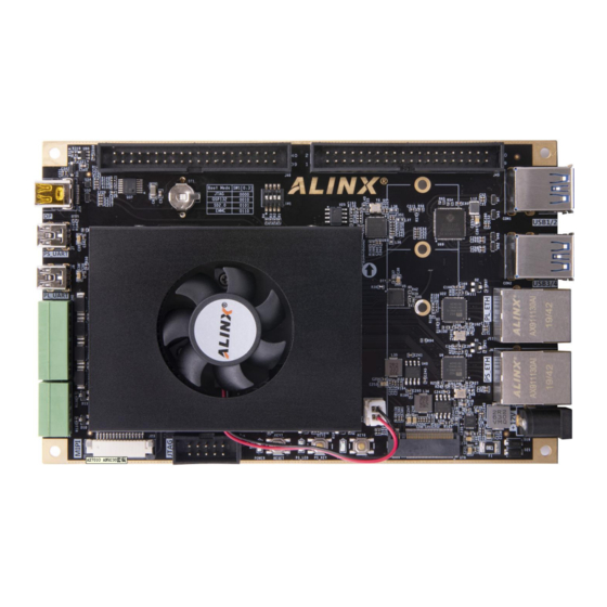
Page 57: Part 3.19: Alinx Customized Fan
BANK65 of Core Board Part 3.19: ALINX Customized Fan Because AXU4EV-E generates a lot of heat when it works normally, we add a heat sink and fan to the chip on the board to prevent the chip from overheating. The control of the fan is controlled by the ZYNQ chip. The control pin is connected to the IO of the BANK43 (AA11). -
Page 58: Part 3.20: Carrier Board Size Dimension
ZYNQ Ultrascale + FPGA Board AXU4EV-E User Manual Figure 3-16-1:Fan Design Schematic The fan has been screwed to the AXUEG FPGA development board before leaving the factory. The power of the fan is connected to the socket of J24. The red is positive and the black is negative.
Need help?
Do you have a question about the AXU4EV-E and is the answer not in the manual?
Questions and answers