Table of Contents
Advertisement
Quick Links
Advertisement
Table of Contents

Related Manuals for Alinx AXU7EV


Summary of Contents for Alinx AXU7EV
- Page 1 ZYNQ UltraScale+ FPGA Development Board AXU7EV User Manual...
-
Page 2: Version Record
ZYNQ Ultrascale + FPGA Board AXU7EV User Manual Version Record Version Date Release By Description Rev 1.1 2021-07-28 Rachel Zhou First Release Amazon Store: https://www.amazon.com/alinx 2 / 68... -
Page 3: Table Of Contents
ZYNQ Ultrascale + FPGA Board AXU7EV User Manual Table of Contents Version Record.......................2 Part 1: FPGA Development Board Introduction..........6 Part 2: ACU7EV Core Board................11 Part 2.1: ACU7EV Core Board Introduction..........11 Part 2.2: ZYNQ Chip...................12 Part 2.3: DDR4 DRAM................14 Part 2.4: QSPI Flash...................23... - Page 4 ZYNQ Ultrascale + FPGA Board AXU7EV User Manual Part 3.15: 485 Communication Interface..........60 Part 3.16: JTAG Debug Port..............61 Part 3.17: Real-time Clock.................62 Part 3.18: EEPROM and Temperature Sensor........63 Part 3.19: User LEDs..................64 Part 3.20: Keys.................... 65 Part 3.21: DIP Switch Configuration............65 Part 3.22: Power Supply................
- Page 5 ZYNQ Ultrascale + FPGA Board AXU7EV User Manual This MPSoCs FPGA development platform adopts the core board + carrier board mode, which is convenient for users to use the core board for secondary development. The core board uses XILINX Zynq UltraScale+ EV chip ZU7EV...
-
Page 6: Part 1: Fpga Development Board Introduction
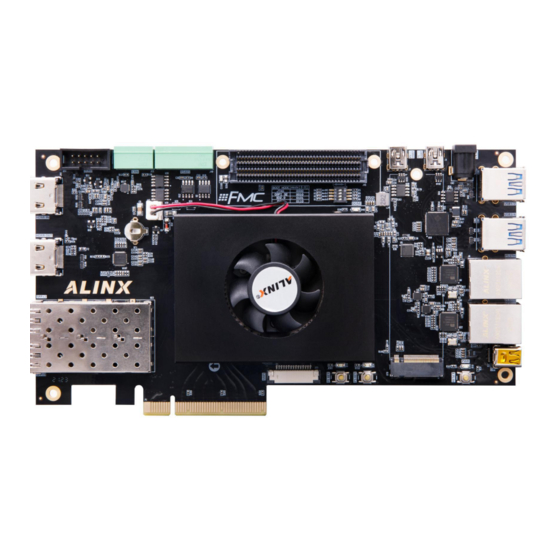
ZYNQ Ultrascale + FPGA Board AXU7EV User Manual Part 1: FPGA Development Board Introduction The entire structure of the AXU7EV PGA development board is inherited from our consistent core board + carrier board model. A high-speed inter-board connector is used between the core board and the carrier board. - Page 7 ZYNQ Ultrascale + FPGA Board AXU7EV User Manual Figure 1-1-1: The Schematic Diagram of the AXU7EV Through this diagram, you can see the interfaces and functions that the AXU7EV FPGA Development Board contains: ZU7EV core board It consists of ZU7EV +4GB DDR4 (PS) +4GB DDR4 (PL) +8GB eMMC FLASH + 512Mb QSPI FLASH, and there are 2 crystal oscillators to provide the clock, a single-ended 33.3333MHz crystal oscillator for the...
- Page 8 ZYNQ Ultrascale + FPGA Board AXU7EV User Manual M.2 Interface 1 PCIEx1 standard M.2 interface, used to connect M.2 SSD solid state drives, with a communication speed of up to 6Gbps. DP Output Interface 1 standard Display Port output display interface, used for video image display.
- Page 9 FMC Expansion Interface 1 standard FMC LPC expansion port, which can be connected to various FMC modules of XILINX or ALINX (HDMI input and output modules, binocular camera modules, high-speed AD modules, etc.). CAN Communication Interface Two-way CAN bus interface, using TI's SN65HVD232 chip, the interface uses 4Pin green terminal blocks.
- Page 10 ZYNQ Ultrascale + FPGA Board AXU7EV User Manual On-board temperature and humidity sensor chip LM75, used to detect the temperature and humidity of the surrounding environment around the FPGA development board EEPROM One EEPROM 24LC04 with I2C interface Real Time Clock (RTC) 1 built-in RTC real-time clock ...
-
Page 11: Part 2: Acu7Ev Core Board
ZYNQ Ultrascale + FPGA Board AXU7EV User Manual Part 2: ACU7EV Core Board Part 2.1: ACU7EV Core Board Introduction ACU7EV (core board model, the same below) FPGA core board, ZYNQ chip is based on XCZU7EV-2FFVB1156I of XILINX company Zynq UltraScale+ MPSoCs EG Family. -
Page 12: Part 2.2: Zynq Chip
ZYNQ Ultrascale + FPGA Board AXU7EV User Manual Figure 2-1-1: ACU7EV Core Board (Front View) Part 2.2: ZYNQ Chip The FPGA core board ACU7EV uses Xilinx's Zynq UltraScale+ MPSoCs EV family chip, module XCZU7EV-2FFVB1156I. The PS system of the ZU7EV chip integrates 4 ARM Cortex™-A53 processors with a speed of up to 1.3Ghz... - Page 13 ZYNQ Ultrascale + FPGA Board AXU7EV User Manual Figure 2-2-1: Overall Block Diagram of the ZYNQ ZU7EV Chip The main parameters of the PS system part are as follows: ARM quad-core Cortex ™ -A53 processor, speed up to 1.3GHz, each...
-
Page 14: Part 2.3: Ddr4 Dram
ZYNQ Ultrascale + FPGA Board AXU7EV User Manual Static storage interface, support NAND, 2xQuad-SPI FLASH. High-speed connection interface, support PCIe Gen2 x 4, 2 x USB3.0, Sata 3.1, Display Port, 4 x Tri-mode, Gigabit Ethernet Common connection interfaces: 2 x USB2.0, 2 x SD/SDIO, 2 x UART, 2 x CAN 2.0B, 2 x I2C, 2 x SPI, 4 x 32b GPIO... - Page 15 ZYNQ Ultrascale + FPGA Board AXU7EV User Manual of 4GB. The maximum operating speed of the DDR4 SDRAM on the PS side can reach 1200MHz (data rate 2400Mbps), and the 4 DDR4 storage systems are directly connected to the memory interface of the PS BANK504. The...
- Page 16 ZYNQ Ultrascale + FPGA Board AXU7EV User Manual The hardware connection of DDR4 SDRAM on the PL Side is shown in Figure 2-3-2: Figure 2-3-2: DDR4 DRAM schematic diagram PS Side DDR4 DRAM pin assignment: Signal Name Pin Name Pin Number...
- Page 17 ZYNQ Ultrascale + FPGA Board AXU7EV User Manual PS_DDR4_DQS7_N PS_DDR_DQS_N7_504 PS_DDR4_DQS7_P PS_DDR_DQS_P7_504 PS_DDR4_DQ0 PS_DDR_DQ0_504 AP27 PS_DDR4_DQ1 PS_DDR_DQ1_504 AP25 PS_DDR4_DQ2 PS_DDR_DQ2_504 AP26 PS_DDR4_DQ3 PS_DDR_DQ3_504 AM26 PS_DDR4_DQ4 PS_DDR_DQ4_504 AP24 PS_DDR4_DQ5 PS_DDR_DQ5_504 AL25 PS_DDR4_DQ6 PS_DDR_DQ6_504 AM25 PS_DDR4_DQ7 PS_DDR_DQ7_504 AM24 PS_DDR4_DQ8 PS_DDR_DQ8_504 AM28 PS_DDR4_DQ9...
- Page 18 ZYNQ Ultrascale + FPGA Board AXU7EV User Manual PS_DDR4_DQ34 PS_DDR_DQ34_504 AC29 PS_DDR4_DQ35 PS_DDR_DQ35_504 AD32 PS_DDR4_DQ36 PS_DDR_DQ36_504 AC31 PS_DDR4_DQ37 PS_DDR_DQ37_504 AE30 PS_DDR4_DQ38 PS_DDR_DQ38_504 AC28 PS_DDR4_DQ39 PS_DDR_DQ39_504 AE29 PS_DDR4_DQ40 PS_DDR_DQ40_504 AC27 PS_DDR4_DQ41 PS_DDR_DQ41_504 AA27 PS_DDR4_DQ42 PS_DDR_DQ42_504 AA28 PS_DDR4_DQ43 PS_DDR_DQ43_504 AB28 PS_DDR4_DQ44 PS_DDR_DQ44_504...
- Page 19 ZYNQ Ultrascale + FPGA Board AXU7EV User Manual PS_DDR4_DM6 PS_DDR_DM6_504 AC32 PS_DDR4_DM7 PS_DDR_DM7_504 PS_DDR4_A0 PS_DDR_A0_504 AN34 PS_DDR4_A1 PS_DDR_A1_504 AM34 PS_DDR4_A2 PS_DDR_A2_504 AM33 PS_DDR4_A3 PS_DDR_A3_504 AL34 PS_DDR4_A4 PS_DDR_A4_504 AL33 PS_DDR4_A5 PS_DDR_A5_504 AK33 PS_DDR4_A6 PS_DDR_A6_504 AK30 PS_DDR4_A7 PS_DDR_A7_504 AJ30 PS_DDR4_A8 PS_DDR_A8_504 AJ31...
- Page 20 ZYNQ Ultrascale + FPGA Board AXU7EV User Manual PL_DDR4_DQS0_P IO_L10P_T1U_N6_QBC_AD4P_67 PL_DDR4_DQS1_N IO_L4N_T0U_N7_DBC_AD7N_67 PL_DDR4_DQS1_P IO_L4P_T0U_N6_DBC_AD7P_67 PL_DDR4_DQS2_N IO_L16N_T2U_N7_QBC_AD3N_67 PL_DDR4_DQS2_P IO_L16P_T2U_N6_QBC_AD3P_67 PL_DDR4_DQS3_N IO_L22N_T3U_N7_DBC_AD0N_67 PL_DDR4_DQS3_P IO_L22P_T3U_N6_DBC_AD0P_67 PL_DDR4_DQS4_N IO_L16N_T2U_N7_QBC_AD3N_68 PL_DDR4_DQS4_P IO_L16P_T2U_N6_QBC_AD3P_68 PL_DDR4_DQS5_N IO_L22N_T3U_N7_DBC_AD0N_68 PL_DDR4_DQS5_P IO_L22P_T3U_N6_DBC_AD0P_68 PL_DDR4_DQS6_N IO_L10N_T1U_N7_QBC_AD4N_68 PL_DDR4_DQS6_P IO_L10P_T1U_N6_QBC_AD4P_68 PL_DDR4_DQS7_N IO_L4N_T0U_N7_DBC_AD7N_68 PL_DDR4_DQS7_P IO_L4P_T0U_N6_DBC_AD7P_68 PL_DDR4_DQ0 IO_L9N_T1L_N5_AD12N_67...
- Page 21 ZYNQ Ultrascale + FPGA Board AXU7EV User Manual PL_DDR4_DQ21 IO_L14N_T2L_N3_GC_67 PL_DDR4_DQ22 IO_L17N_T2U_N9_AD10N_67 PL_DDR4_DQ23 IO_L14P_T2L_N2_GC_67 PL_DDR4_DQ24 IO_L24N_T3U_N11_67 PL_DDR4_DQ25 IO_L21N_T3L_N5_AD8N_67 PL_DDR4_DQ26 IO_L23P_T3U_N8_67 PL_DDR4_DQ27 IO_L21P_T3L_N4_AD8P_67 PL_DDR4_DQ28 IO_L24P_T3U_N10_67 PL_DDR4_DQ29 IO_L20P_T3L_N2_AD1P_67 PL_DDR4_DQ30 IO_L23N_T3U_N9_67 PL_DDR4_DQ31 IO_L20N_T3L_N3_AD1N_67 PL_DDR4_DQ32 IO_L18N_T2U_N11_AD2N_68 PL_DDR4_DQ33 IO_L17P_T2U_N8_AD10P_68 PL_DDR4_DQ34 IO_L17N_T2U_N9_AD10N_68 PL_DDR4_DQ35 IO_L14P_T2L_N2_GC_68 PL_DDR4_DQ36 IO_L18P_T2U_N10_AD2P_68...
- Page 22 ZYNQ Ultrascale + FPGA Board AXU7EV User Manual PL_DDR4_DQ57 IO_L6N_T0U_N11_AD6N_68 PL_DDR4_DQ58 IO_L5P_T0U_N8_AD14P_68 PL_DDR4_DQ59 IO_L2P_T0L_N2_68 PL_DDR4_DQ60 IO_L6P_T0U_N10_AD6P_68 PL_DDR4_DQ61 IO_L3P_T0L_N4_AD15P_68 PL_DDR4_DQ62 IO_L2N_T0L_N3_68 PL_DDR4_DQ63 IO_L3N_T0L_N5_AD15N_68 PL_DDR4_DM0 IO_L7P_T1L_N0_QBC_AD13P_67 PL_DDR4_DM1 IO_L1P_T0L_N0_DBC_67 PL_DDR4_DM2 IO_L13P_T2L_N0_GC_QBC_67 PL_DDR4_DM3 IO_L19P_T3L_N0_DBC_AD9P_67 PL_DDR4_DM4 IO_L13P_T2L_N0_GC_QBC_68 PL_DDR4_DM5 IO_L19P_T3L_N0_DBC_AD9P_68 PL_DDR4_DM6 IO_L7P_T1L_N0_QBC_AD13P_68 PL_DDR4_DM7 IO_L1P_T0L_N0_DBC_68 PL_DDR4_A0 IO_L10P_T1U_N6_QBC_AD4P_66...
-
Page 23: Part 2.4: Qspi Flash
ZYNQ Ultrascale + FPGA Board AXU7EV User Manual PL_DDR4_BG0 IO_L7P_T1L_N0_QBC_AD13P_66 AK13 PL_DDR4_CAS_B IO_L8N_T1L_N3_AD5N_66 AL10 PL_DDR4_CKE IO_L15P_T2L_N4_AD11P_66 AG13 PL_DDR4_CS_B IO_L9P_T1L_N4_AD12P_66 AK12 PL_DDR4_CLK_N IO_L13N_T2L_N1_GC_QBC_66 AJ12 PL_DDR4_CLK_P IO_L13P_T2L_N0_GC_QBC_66 AH12 Part 2.4: QSPI Flash The FPGA core board ACU7EV is equipped with two 256MBit Quad-SPI FLASH chip to form an 8-bit bandwidth data bus, the flash model is MT25QU256ABA1EW9, which uses the 1.8V CMOS voltage standard. -
Page 24: Part 2.5: Emmc Flash
ZYNQ Ultrascale + FPGA Board AXU7EV User Manual Figure 2-4-1: QSPI Flash in the schematic Configure chip pin assignments: Signal Name Pin Name Pin Number MIO0_QSPI0_SCLK PS_MIO0_500 MIO1_QSPI0_IO1 PS_MIO1_500 MIO2_QSPI0_IO2 PS_MIO2_500 MIO3_QSPI0_IO3 PS_MIO3_500 MIO4_QSPI0_IO0 PS_MIO4_500 MIO5_QSPI0_SS_B PS_MIO5_500 MIO10_QSPI1_IO2 PS_MIO10_500 MIO11_QSPI1_IO3... - Page 25 ZYNQ Ultrascale + FPGA Board AXU7EV User Manual FLASH chip, the model is MTFC8GAKAJCN-4M, it supports the HS-MMC interface of the JEDEC e-MMC V5.0 standard, and the level supports 1.8V or 3.3V. The data width of eMMC FLASH and ZYNQ connection is 8bit. Due to the...
-
Page 26: Part 2.6: Clock Configuration
ZYNQ Ultrascale + FPGA Board AXU7EV User Manual MMC_DAT1 PS_MIO14_500 MMC_DAT2 PS_MIO15_500 MMC_DAT3 PS_MIO16_500 MMC_DAT4 PS_MIO17_500 MMC_DAT5 PS_MIO18_500 MMC_DAT6 PS_MIO19_500 MMC_DAT7 PS_MIO20_500 MMC_RSTN PS_MIO23_500 Part 2.6: Clock configuration The core board provides reference clock and RTC real-time clock for PS system and PL logic respectively, so that PS system and PL logic can work independently. - Page 27 ZYNQ Ultrascale + FPGA Board AXU7EV User Manual diagram is shown in Figure 2-6-2: Figure 2-6-2: Passive Crystal Oscillator for RTC Clock pin assignment: Signal Name PS_PADI_503 PS_PADO_503 PS System Clock Source The X1 crystal on the core board provides a 33.333MHz clock input for the PS part.
-
Page 28: Part 2.7: Power Supply
ZYNQ Ultrascale + FPGA Board AXU7EV User Manual PL System Clock Source The core board provides a differential 200MHz PL system clock source for the reference clock of the DDR4 controller. The crystal oscillator output is connected to the global clock (MRCC) of PL BANK64. This global clock can be used to drive the DDR4 controller and user logic circuits in the FPGA. - Page 29 ZYNQ Ultrascale + FPGA Board AXU7EV User Manual Amazon Store: https://www.amazon.com/alinx 29 / 68...
-
Page 30: Part 2.8: Acu7Ev Core Board Size Dimension
ZYNQ Ultrascale + FPGA Board AXU7EV User Manual Part 2.8: ACU7EV Core Board Size Dimension Figure 2-8-1: ACU7EV Core Board Size Dimension Part 2.9: Board to Board Connectors pin assignment The core board has a total of four high-speed expansion ports. It uses four 120-pin inter-board connectors (J29/J30/J31/J32) to connect to the carrier board. - Page 31 ZYNQ Ultrascale + FPGA Board AXU7EV User Manual J29 Pin Signal Name J29 Pin Signal Name Pin Number Number +12V +12V +12V +12V +12V +12V +12V +12V +12V +12V +12V +12V B88_L2_N B88_L1_N B88_L2_P B88_L1_P B88_L5_N B88_L4_N B88_L5_P B88_L4_P B88_L8_N...
- Page 32 ZYNQ Ultrascale + FPGA Board AXU7EV User Manual B87_L4_N B28_L7_N B87_L4_P B28_L7_P B28_L20_N B28_L9_N B28_L20_P B28_L9_P B28_L19_N B28_L10_N B28_L19_P B28_L10_P B28_L21_N B28_L22_N B28_L21_P B28_L22_P B28_L24_N B28_L15_N B28_L24_P B28_L15_P B28_L23_N B28_L17_N B28_L23_P B28_L17_P PS_MIO43 PS_MIO26 PS_MIO32 PS_MIO27 PS_MIO35 PS_MIO31 PS_MIO36 PS_MIO40...
- Page 33 ZYNQ Ultrascale + FPGA Board AXU7EV User Manual B28_L11_N SD_CMD B28_L11_P SD_D0 B28_L13_P SD_D1 B28_L13_N SD_CLK B28_L12_N SD_CD B28_L12_P B28_L3_P USB_STP B28_L3_N USB_DIR USB_CLK USB_NXT USB_DATA0 USB_DATA1 B28_L18_N USB_DATA2 B28_L18_P USB_DATA3 B28_L14_N USB_DATA4 B28_L14_P USB_DATA5 USB_DATA6 USB_DATA7 PHY1_TXD0 PHY1_TXD1 PHY1_TXD2...
- Page 34 ZYNQ Ultrascale + FPGA Board AXU7EV User Manual FPGA_TDI PHY1_RXCK FPGA_TMS PHY1_MDC FPGA_TDO PHY1_MDIO 505_RX3_N 505_TX3_N 505_RX3_P 505_TX3_P 505_RX2_N 505_TX2_N 505_RX2_P 505_TX2_P 505_RX1_N 505_TX1_N 505_RX1_P 505_TX1_P 505_RX0_N 505_TX0_N 505_RX0_P 505_TX0_P 505_CLK0_N 505_CLK1_N 505_CLK0_P 505_CLK1_P 505_CLK2_N 505_CLK3_N 505_CLK2_P 505_CLK3_P Pin assignment of board to board connector J31...
- Page 35 ZYNQ Ultrascale + FPGA Board AXU7EV User Manual B65_L12_N AJ22 B65_L3_N AP22 B65_L12_P AJ21 B65_L3_P AP21 B65_L5_N AP23 B65_L7_N AL21 B65_L5_P AN22 B65_L7_P AL20 B65_L10_N AK23 B65_L21_N AE20 B65_L10_P AK22 B65_L21_P AD20 B65_L14_N AH21 B65_L6_N AN23 B65_L14_P AG21 B65_L6_P AM23...
- Page 36 ZYNQ Ultrascale + FPGA Board AXU7EV User Manual B64_L21_N AB15 B64_L8_N AL15 B64_L7_P AM16 B64_L12_P AJ16 B64_L7_N AM15 B64_L12_N AJ15 B64_L10_P AK15 B64_L16_P AH14 B64_L10_N AK14 B64_L16_N AJ14 B64_L20_P AC17 B64_L15_P AE17 B64_L20_N AC16 B64_L15_N AF17 B64_L18_P AG15 B64_L17_P AF16...
- Page 37 ZYNQ Ultrascale + FPGA Board AXU7EV User Manual 224_RX0_P 224_TX0_P 224_RX0_N 224_TX0_N 224_RX1_P 224_TX1_P 224_RX1_N 224_TX1_N 224_RX2_P 224_TX2_P 224_RX2_N 224_TX2_N 224_RX3_P 224_TX3_P 224_RX3_N 224_TX3_N 224_CLK1_P AA10 224_CLK0_P 224_CLK1_N 224_CLK0_N 225_CLK1_P 225_CLK0_P 225_CLK1_N 225_CLK0_N 225_RX1_P 225_RX0_P 225_RX1_N 225_RX0_N 225_TX1_P 225_TX0_P 225_TX1_N...
- Page 38 ZYNQ Ultrascale + FPGA Board AXU7EV User Manual 226_RX2_P 226_TX2_P 226_RX2_N 226_TX2_N 226_RX1_P 226_TX1_P 226_RX1_N 226_TX1_N 226_RX0_P 226_TX0_P 226_RX0_N 226_TX0_N Amazon Store: https://www.amazon.com/alinx 38 / 68...
-
Page 39: Part 3: Carrier Board
2 LED lights 2 Keys Part 3.2: PCIe Slot There is a PCIe3.0 x8 interface on the AXU7EV carrier board, and eight pairs of transceivers are connected to the PCIEx8, which can realize PCIe x 8, Amazon Store: https://www.amazon.com/alinx... - Page 40 ZYNQ Ultrascale + FPGA Board AXU7EV User Manual PCIe x 4, PCIe x 2, PCIe x 2 data communication. The transceiver signal of the PCIe interface is directly connected to the GTH transceiver of FPGA BANK223, BANK224, and the single-channel communication rate can be as high as 8G bit bandwidth.
- Page 41 ZYNQ Ultrascale + FPGA Board AXU7EV User Manual PCIE Channel 2 Data Receive Negative PCIE_RX2_N 223_RX2_N PCIE Channel 2 Data Receive Positive PCIE_RX2_P 223_RX2_P PCIE Channel 3 Data Receive Negative PCIE_RX3_N 223_RX3_N PCIE Channel 3 Data Receive Positive PCIE_RX3_P 223_RX3_P...
-
Page 42: Part 3.3: M.2 Interface
ZYNQ Ultrascale + FPGA Board AXU7EV User Manual Part 3.3: M.2 Interface The AXU7EV FPGA development board is equipped with a PCIE x1 standard M.2 interface for connecting M.2 SSD solid state drives, with a communication speed of up to 6Gbps. The M.2 interface uses the M key slot, which only supports PCI-E, not SATA. -
Page 43: Part 3.4: Dp Interface
PCIE_RSTN_MIO37 PS_MIO37 Part 3.4: DP Interface The AXU7EV FPGA development board has a standard DisplayPort output display interface for video image display. The interface supports VESA DisplayPort V1.2a output standard, up to 4K x 2K@30Fps output, supports Y-only, YCbCr444, YCbCr422, YCbCr420 and RGB video formats, each color supports 6, 8, 10, or 12 bits. -
Page 44: Part 3.5: Usb3.0 Interface
PS_MIO28 Part 3.5: USB3.0 Interface There are 4 USB3.0 ports on the AXU7EV carrier board, supporting the HOST working mode, and the data transmission speed is up to 5.0Gb/s. USB3.0 is connected through the PIPE3 interface, and USB2.0 is connected to the external USB3320C chip through the ULPI interface to realize high-speed USB3.0 and USB2.0 data communication. - Page 45 ZYNQ Ultrascale + FPGA Board AXU7EV User Manual Figure 3-4-1: USB3.0 Interface Schematic USB Interface Pin Assignment: Signal Name Pin Name Pin Number Description USB3.0 Data Transmit Positive USB_SSTXP 505_TX1_N USB_SSTXN USB3.0 Data Transmit Negative 505_TX1_P USB3.0 Data Receive Positive...
-
Page 46: Part 3.6: Hdmi Output Interface
ZYNQ Ultrascale + FPGA Board AXU7EV User Manual Part 3.6: HDMI Output Interface There is one HDMI Output Interface on the carrier board. The HMDI chip uses TI's SN75DP159 chip to realize the TMDS level conversion redriver and receiver equalization function, and increase the signal driving capability. The HDMI interface supports up to 4K@60Hz output. -
Page 47: Part 3.7: Hdmi Input Interface
ZYNQ Ultrascale + FPGA Board AXU7EV User Manual HDMI Video Output Signal Data 1 HDMI_TX0_D1N 226_TX1_N Negative HDMI Video Output Signal Data 1 HDMI_TX0_D1P 226_TX1_P Positive HDMI Video Output Signal Data 2 HDMI_TX0_D2N 226_TX2_N Negative HDMI Video Output Signal Data 2... - Page 48 ZYNQ Ultrascale + FPGA Board AXU7EV User Manual Figure 3-7-1: HDMI Input Interface Schematic ZYNQ pin assignment: Signal Name FPGA Pin Name FPGA Description Numb HDMI Video Input Signal Data 0 HDMI_IN0_RX_0N 226_RX0_N Negative HDMI Video Input Signal Data 0...
-
Page 49: Part 3.8: Gigabit Ethernet Interface
B88_L9_P Part 3.8: Gigabit Ethernet Interface There are 2 Gigabit Ethernet ports on the AXU7EV carrier board, one is connected to the PS end, and the other is connected to the PL end. The GPHY chip uses Micrel's KSZ9031RNX Ethernet PHY chip to provide users with... - Page 50 ZYNQ Ultrascale + FPGA Board AXU7EV User Manual CLK125_EN Enable 125Mhz clock output selection Enable LED_MODE LED light mode configuration Single LED light mode 10/100/1000 adaptive, compatible Link adaptation and full duplex MODE0~MODE3 with full-duplex, half-duplex configuration Table 3-8-1: PHY chip default configuration value...
- Page 51 ZYNQ Ultrascale + FPGA Board AXU7EV User Manual Ethernet 1 Transmit data bit0 PHY1_TXD0 PHY1_TXD0 Ethernet 1 Transmit data bit1 PHY1_TXD1 PHY1_TXD1 Ethernet 1 Transmit data bit2 PHY1_TXD2 PHY1_TXD2 Ethernet 1 Transmit data bit3 PHY1_TXD3 PHY1_TXD3 Ethernet 1 Transmit Enable Signal...
-
Page 52: Part 3.9: Usb To Serial Port
ZYNQ Ultrascale + FPGA Board AXU7EV User Manual Part 3.9: USB to Serial Port The AXU7EV carrier board is equipped with two Uart to USB ports, one is connected to the PS end, and one is connected to the PL end. The conversion chip uses Silicon Labs CP2102GM's USB-UAR chip, and the USB interface is a MINI USB interface. -
Page 53: Part 3.10: Sfp Interface
ZYNQ Ultrascale + FPGA Board AXU7EV User Manual Part 3.10: SFP Interface The AXU7EV FPGA carrier board has two optical interfaces. Users can purchase SFP optical modules (1.25G, 2.5G, 10G optical modules on the market) and insert them into these two optical interfaces for optical data communication. -
Page 54: Part 3.11: Sd Card Slot Interface
Detect Signal Part 3.11: SD Card Slot Interface The AXU7EV FPGA Development Board contains a Micro SD card interface to provide user access to the SD card memory, the BOOT program for the ZU7EV chip, the Linux operating system kernel, the file system and other user data files. -
Page 55: Part 3.12: Mipi Camera Interface
SD_CMD Part 3.12: MIPI Camera Interface The AXU7EV carrier board includes a MIPI camera interface, which can be used to connect with the ALINX Brand MIPI OV5640 camera module AN5641. MIPI interface 15PIN FPC connector, 2 LANE data and 1 pair of clock, connected to the differential IO pin of BANK65. -
Page 56: Part 3.13: Fmc Interface
Part 3.13: FMC Interface The AXU7EV FPGA Carrier board has a standard FMC LPC expansion port that can be connected to various FMC modules of XILINX or ALINX (HDMI input and output modules, binocular camera modules, high-speed AD modules, etc.). The FMC expansion port contains 36 pairs of differential IO signals and 8 pairs of GTX Transceivers. - Page 57 ZYNQ Ultrascale + FPGA Board AXU7EV User Manual Figure 3-13-1: FMC Schematic FMC connector pin assignment Signal Name ZYNQ Pin Name ZYNQ Pin Description Number FMC Transceiver Data Transmission 0 FMC_DP0_C2M_N 225_TX1_N Negative FMC Transceiver Data Transmission 0 FMC_DP0_C2M_P 225_TX1_P...
- Page 58 ZYNQ Ultrascale + FPGA Board AXU7EV User Manual FMC Reference 2 Data N FMC_LA02_N B28_L16_N FMC Reference 2 Data P FMC_LA02_P B28_L16_P FMC Reference 3 Data N FMC_LA03_N B28_L12_N FMC Reference 3 Data P FMC_LA03_P B28_L12_P FMC Reference 4 Data N...
- Page 59 ZYNQ Ultrascale + FPGA Board AXU7EV User Manual FMC Reference 19 Data N FMC_LA19_N B64_L2_N AP13 FMC Reference 19 Data P FMC_LA19_P B64_L2_P AN13 FMC Reference 20 Data N FMC_LA20_N B64_L4_N AN14 FMC Reference 20 Data P FMC_LA20_P B64_L4_P AM14...
-
Page 60: Part 3.14: Can Communication Interface
ZYNQ Ultrascale + FPGA Board AXU7EV User Manual Part 3.14: CAN Communication Interface There are 2 CAN communication interfaces on the AXU7EV carrier board, which are connected to the MIO interface of the BANK501 on the PS system side. The CAN transceiver chip selected TI's SN65HVD232C chip for user CAN communication services. -
Page 61: Part 3.16: Jtag Debug Port
PL_485_DE2 B88_L10_P Part 3.16: JTAG Debug Port The JTAG interface is reserved on the AXU7EV carrier board for downloading ZYNQ UltraScale+ programs or firmware programs to FLASH. In order to not damage the ZYNQ UltraScale+ chip by plugging and unplugging under power, we aded a protection diode to the JTAG signal to ensure that the Amazon Store: https://www.amazon.com/alinx... -
Page 62: Part 3.17: Real-Time Clock
ZYNQ Ultrascale + FPGA Board AXU7EV User Manual signal voltage is within the range accepted by the FPGA and avoid damage to the ZYNQ UltraScale+ chip. Figure 3-14-1: JTAG Interface Schematic Part 3.17: Real-time Clock The ZU7EV chip has the function of an RTC real-time clock, with timing functions such as year, month, day, hour, minute, and second, and week. -
Page 63: Part 3.18: Eeprom And Temperature Sensor
PS terminal through the I2C bus. A high-precision, low-power, digital temperature sensor chip is installed on the AXU7EV FPGA development board, and the model is LM75 from ON Semiconductor. The temperature accuracy of the LM75 chip is 0.5 degrees. -
Page 64: Part 3.19: User Leds
PS_MIO35 Part 3.19: User LEDs There are 4 LEDs on the AXU7EV Carrier board. including 1 power indicator light, 1 DONE indicator, 1 PS control indicator, and 1 PL control indicator. The user can control the on and off through the program. The... -
Page 65: Part 3.20: Keys
ZYNQ Ultrascale + FPGA Board AXU7EV User Manual Part 3.20: Keys There are 1 reset KEY RESET and 2 user KEYs on the AXU7EV carrier board. The reset signal is connected to the reset chip input of the core board ACU7EV, and the user can use this reset KEY to reset the ZYNQ system. -
Page 66: Part 3.22: Power Supply
ON,OFF, OFF, ON Part 3.22: Power Supply The power input voltage of the AXU7EV development board is DC12V. In the carrier board, the DC12V is converted into +5V, +3.3V, +1.8V, through one-way DC/DC power chip TPS54620 and two-way DC/DC power chip MP2323/MP1482. -
Page 67: Part 3.23: Alinx Customized Fan
ZYNQ Ultrascale + FPGA Board AXU7EV User Manual The functions of each power distribution are shown in the following table: Power Function +5.0V USB power supply +1.8V Ethernet, USB2.0 +3.3V Ethernet, USB2.0, M.2, SD, DP, CAN, RS485 Part 3.23: ALINX Customized Fan Because ZU7EV generates a lot of heat when it works normally, we add a heat sink and fan to the chip on the board to prevent the chip from overheating. -
Page 68: Part 3.24: Carrier Board Size Dimension
ZYNQ Ultrascale + FPGA Board AXU7EV User Manual Part 3.24: Carrier Board Size Dimension Figure 3-24-1: Top View Amazon Store: https://www.amazon.com/alinx 68 / 68...
Need help?
Do you have a question about the AXU7EV and is the answer not in the manual?
Questions and answers