Xilinx Kintex-7 FPGA KC705 Getting Started Manual
Vivado design suite 2013.2
Hide thumbs
Also See for Kintex-7 FPGA KC705:
- User manual (66 pages) ,
- Getting started manual (29 pages) ,
- Getting started (24 pages)

Related Manuals for Xilinx Kintex-7 FPGA KC705


Summary of Contents for Xilinx Kintex-7 FPGA KC705
- Page 1 Kintex-7 FPGA KC705 Evaluation Kit (Vivado Design Suite 2013.2) Getting Started Guide UG883 (v4.0.1) May 28, 2014 XPM 0402894-05...
- Page 2 (including loss of data, profits, goodwill, or any type of loss or damage suffered as a result of any action brought by a third party) even if such damage or loss was reasonably foreseeable or Xilinx had been advised of the possibility of the same.
-
Page 3: Revision History
The document was updated for Vivado™ Design Suite 2012.4. Agile Mixed Signal is now Analog Mixed Signal. The USB stick is removed from the kit and instead, design files are accessible from the Docs & Designs tab at www.xilinx.com/kc705. Removing the USB stick affected many sections including these: •... - Page 4 KC705 Getting Started Guide www.xilinx.com UG883 (v4.0.1) May 28, 2014...
- Page 5 ............. 3 Getting Started with the Kintex-7 FPGA KC705 Evaluation Kit (Vivado Design Suite 2013.2) Introduction .
- Page 6 KC705 Getting Started Guide Send Feedback UG883 (v4.0.1) May 28, 2014...
-
Page 7: Introduction
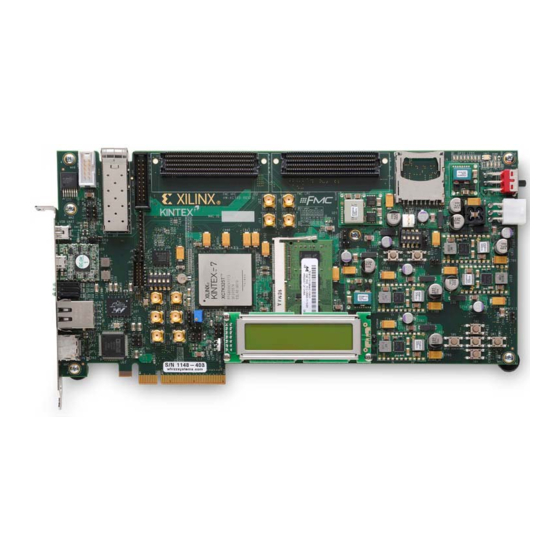
Getting Started with the Kintex-7 FPGA KC705 Evaluation Kit (Vivado Design Suite 2013.2) Introduction The Kintex®-7 FPGA KC705 evaluation kit provides a comprehensive, high-performance development and demonstration platform using the Kintex-7 FPGA family for high-bandwidth and high-performance applications in multiple market segments. The kit enables designing with DDR3, I/O expansion through FMC, and common serial standards, such as PCI Express®, XAUI, and proprietary serial standards through the SMA... -
Page 8: Kit Contents
• KC705 Reference Design User Guide (UG845) (online on product page) • Kintex-7 FPGA KC705 Base Targeted Reference Design User Guide (Vivado Design Suite 2012.4) (UG882) (online on product page) • Board design files including schematics, Gerber files, and BOM (online on product page) •... -
Page 9: Hardware Test Setup Requirements
Basic Hardware Bring-up Using the BIST Basic Hardware Bring-up Using the BIST The built-in self-test (BIST) tests many of the features offered by the Kintex-7 FPGA KC705 evaluation kit. The test is stored in the nonvolatile BPI Linear Flash memory, and configures the FPGA when the mode and upper flash address pins on the board are set for Master BPI. -
Page 10: Hardware Test Board Setup Requirements
12V power adapter included with the KC705 evaluation kit. Table 1: Switch & Jumper Settings Switch Setting Board Power slide-switch SW15 User GPIO DIP switch SW11 Configuration Mode switch SW13 www.xilinx.com KC705 Getting Started Guide Send Feedback UG883 (v4.0.1) May 28, 2014... - Page 11 Figure X-Ref Target - Figure 3 UG883_03_011912 Figure 3: KC705 with the UART and Power Cable Attached Install the power cable. Switch the KC705 board power to ON. KC705 Getting Started Guide www.xilinx.com Send Feedback UG883 (v4.0.1) May 28, 2014...
- Page 12 Find and right-click the Silicon Labs device in the list. Then select Properties. • Click the Port Settings tab and the Advanced… button. • Select an open COM port between COM1 and COM4. www.xilinx.com KC705 Getting Started Guide Send Feedback UG883 (v4.0.1) May 28, 2014...
- Page 13 Steps and diagrams refer to use with a Windows host PC with the Windows XP or Windows 7 operating system. X-Ref Target - Figure 5 UG883_05_040913 Figure 5: Port Selection on the Device Manager Screen KC705 Getting Started Guide www.xilinx.com Send Feedback UG883 (v4.0.1) May 28, 2014...
- Page 14 Select the relevant tests to run, and observe the results. For more information on the BIST software and additional tutorials, including how to restore the default content of the onboard nonvolatile storage, see the KC705 support website. www.xilinx.com KC705 Getting Started Guide Send Feedback UG883 (v4.0.1) May 28, 2014...
-
Page 15: Ams Bring-Up With The Ams101 Evaluation Card
AMS Bring-up with the AMS101 Evaluation Card AMS Bring-up with the AMS101 Evaluation Card The Xilinx® 7 series FPGAs each feature a 1 MSPS, 12-bit, analog-to-digital converter built into the FPGA for everything from simple analog monitoring to more signal processing intensive tasks like linearization, calibration, oversampling and filtering. -
Page 16: Getting Started
When loading the National Instruments LabView run-time engine, click OK to accept the license agreement. Running the setup program loads the AMS101 Evaluator GUI with the red Xilinx logo on the desktop. After the AMS Evaluator has successfully installed, restart the host PC. - Page 17 Download the design to the FPGA. Installation of ISE Programming tools or Lab Tools is required for downloading the bitstream to the FPGA. Refer to the Vivado Design Suite User Guide: Programming and Debugging (UG908) at http://www.xilinx.com/support/documentation/dt_vivado.htm to obtain information on downloading the design to the FPGA.
- Page 18 For a more extensive explanation of the AMS101 evaluation card and the applicable files, refer to AMS101 Evaluation Platform User Guide (UG886). www.xilinx.com KC705 Getting Started Guide Send Feedback UG883 (v4.0.1) May 28, 2014...
-
Page 19: Advanced Bring-Up Using The Base Targeted Reference Design
64 x Controller 250 MHz 250 MHz Checker VFIFO Controller Raw Packet Data Block Interface Blocks in FPGA Xilinx IP Custom Logic Third Party IP On Board AXI-ST AXI-MM UG883_10_121112 Figure 10: Kintex-7 FPGA Base TRD Block Diagram Note: Figure 10 the arrows indicate AXI interface directions (from master to slave). - Page 20 The software driver runs on the host system. It generates raw data traffic for transmit operations in the S2C direction. It also consumes the data looped back or generated at the application end in the C2S direction. www.xilinx.com KC705 Getting Started Guide Send Feedback...
- Page 21 These are the prerequisites for testing the design in hardware: • KC705 Evaluation board with the Kintex-7 FPGA XC7K325T-2FFG900C device • Design files provided as a zipped collection under the Docs & Designs tab at www.xilinx.com/kc705 include: • Design source files •...
-
Page 22: Board Setup
DIP switch SW13 positions 3, 4, and 5 control which configuration mode. 5 (M0) M2 =0 M1=1 M0=0 – Master BPI M2 =0 M1=0 M0=1 – Master SPI 4 (M1) M2 =1 M1=0 M0=1 – JTAG 3 (M2) www.xilinx.com KC705 Getting Started Guide Send Feedback UG883 (v4.0.1) May 28, 2014... - Page 23 Endpoint to be installed into a larger lane width PCIe connector. X-Ref Target - Figure 12if UG883_12_040913 Figure 12: KC705 Board Plugged into a PCIe x16 Slot KC705 Getting Started Guide www.xilinx.com Send Feedback UG883 (v4.0.1) May 28, 2014...
- Page 24 Note: If the user wishes to boot Linux from the Fedora 16 Live DVD, place the DVD in the PC’s DVD-ROM drive as soon as the PC system is powered on. www.xilinx.com KC705 Getting Started Guide Send Feedback UG883 (v4.0.1) May 28, 2014...
- Page 25 LED 3 — ON if memory calibration is done • LED 4 to LED 7 — Not connected X-Ref Target - Figure 14 UG883_14_121112 Figure 14: Location of GPIO Status LEDs (Indicates TRD Status) KC705 Getting Started Guide www.xilinx.com Send Feedback UG883 (v4.0.1) May 28, 2014...
-
Page 26: Install The Linux Driver
$ lspci The lspci command displays the devices in the PCI and PCI Express buses of the PC. On the bus of the KC705 card slot is the message Communication controller: Xilinx Corporation Device 7042 www.xilinx.com KC705 Getting Started Guide Send Feedback UG883 (v4.0.1) May 28, 2014... - Page 27 BIOS and the Fedora 16 OS. The bus number varies depending on which PC motherboard and slot are used. Figure 16 shows a lspci output for an example system. Xilinx device 7042 has been found by the BIOS on bus number 2 (02:00.0 - bus:dev.function). X-Ref Target - Figure 16 UG883_16_040913 Figure 16: PCI and PCI Express Bus Devices Download the reference design from the Docs &...
- Page 28 Click Run in Terminal to proceed. The application GUI is invoked. Proceed to the next section, Using the Application GUI, to set design parameters and run the TRD. www.xilinx.com KC705 Getting Started Guide Send Feedback UG883 (v4.0.1) May 28, 2014...
- Page 29 Click the System Status tab to verify the status of the KC705 board and the PCIe link (see Figure 19 Table X-Ref Target - Figure 19 UG883_19_121112 Figure 19: Verify Board Status in the Performance Monitor KC705 Getting Started Guide www.xilinx.com Send Feedback UG883 (v4.0.1) May 28, 2014...
- Page 30 Raw Data Path0. b. Click Start Test on Raw Data Path1 as shown in Figure 20. This enables the driver to start generating the data for Raw Data Path1. www.xilinx.com KC705 Getting Started Guide Send Feedback UG883 (v4.0.1) May 28, 2014...
- Page 31 Verify the DMA channel throughput for the Raw Data Path0. Verify the DMA channel throughput for the Raw Data Path1. d. Verify there are no buffer descriptor errors for error-free operation. KC705 Getting Started Guide www.xilinx.com Send Feedback UG883 (v4.0.1) May 28, 2014...
- Page 32 Figure 21: Verify Error-Free Operation in the Performance Monitor The Kintex-7 FPGA PCIe-DMA TRD is now set up and running. Close the Application GUI to unload the software drivers and stop traffic flow. www.xilinx.com KC705 Getting Started Guide Send Feedback...
- Page 33 Figure 22: Launch the Performance Monitor and Status GUI A window prompt appears as shown in Figure 23. Click Run in Terminal to proceed. X-Ref Target - Figure 23 UG883_23_121112 Figure 23: Run k7_lin_trd_quickstart KC705 Getting Started Guide www.xilinx.com Send Feedback UG883 (v4.0.1) May 28, 2014...
- Page 34 Click the Payload Statistics tab to view data transfers on the DMA channels. Click Stop Test to stop data traffic. X-Ref Target - Figure 24 UG883_24_121112 Figure 24: Payload Statistics www.xilinx.com KC705 Getting Started Guide Send Feedback UG883 (v4.0.1) May 28, 2014...
- Page 35 For packet sizes equal to 64 or 128 bytes, the throughput is reduced and might not be visible on the Payload Statistics tab. The exact values can be viewed on the System Status tab. KC705 Getting Started Guide www.xilinx.com Send Feedback UG883 (v4.0.1) May 28, 2014...
- Page 36 Design Suite on a PC. It is not required that tools be installed on the PC system in which the KC705 evaluation board is plugged in by way of the PCIe edge connector. www.xilinx.com KC705 Getting Started Guide Send Feedback...
-
Page 37: Xilinx Resources
The Kintex-7 FPGA KC705 Evaluation Kit Product Page: www.xilinx.com/kc705 The Kintex-7 FPGA KC705 Evaluation Kit Master Answer Record: www.xilinx.com/support/answers/47787.htm Design advisories by software release for the Kintex-7 FPGA KC705 Evaluation Kit: www.xilinx.com/support/#nav=sd-nav-link-179661&tab=tab-bk Kintex-7 FPGA Base Targeted Reference Design Release Notes and Known Issues Master Answer Record: www.xilinx.com/support/answers/45679.htm... -
Page 38: References
Appendix A: Additional Resources UG908, Vivado Design Suite User Guide: Programming and Debugging UG882, Kintex-7 FPGA KC705 Base Targeted Reference Design User Guide (Vivado Design Suite 2012.4) UG886, AMS101 Evaluation Card User Guide PG054, 7 Series FPGAs Integrated Block for PCI Express User Guide... - Page 39 For any breach by Xilinx of this limited warranty, the exclusive remedy of Customer and the sole liability of Xilinx shall be, at the option of Xilinx, to replace or repair the affected products, or to refund to Customer the price of the affected products. The availability of replacement products is subject to product discontinuation policies at Xilinx.
- Page 40 Appendix B: Warranty www.xilinx.com KC705 Getting Started Guide Send Feedback UG883 (v4.0.1) May 28, 2014...
Need help?
Do you have a question about the Kintex-7 FPGA KC705 and is the answer not in the manual?
Questions and answers