Table of Contents
Advertisement
Advertisement
Table of Contents

Related Manuals for Xilinx VCU128


Summary of Contents for Xilinx VCU128
- Page 1 VCU128 Evaluation Board User Guide UG1302 (v1.0) December 21, 2018...
-
Page 2: Table Of Contents
Chapter 3: Board Component Descriptions ........... 18 Overview.............................18 Component Descriptions......................18 Appendix A: VITA 57.4 FMCP Connector Pinouts ......... 93 Overview.............................93 Appendix B: Xilinx Constraints File ..............94 Overview.............................94 Appendix C: Regulatory and Compliance Information ......95 Overview.............................95 CE Directives..........................95 CE Standards.......................... - Page 3 Xilinx Resources.........................97 Documentation Navigator and Design Hubs.................97 References..........................98 Please Read: Important Legal Notices................. 100 UG1302 (v1.0) December 21, 2018 www.xilinx.com Send Feedback VCU128 Board User Guide...
-
Page 4: Revision History
Revision History Revision History The following table shows the revision history for this document. Section Revision Summary 12/21/2018 Version 1.0 Initial Xilinx release. UG1302 (v1.0) December 21, 2018 www.xilinx.com Send Feedback VCU128 Board User Guide... -
Page 5: Chapter 1: Introduction
UltraScale+™ FPGA provides a hardware environment for developing and evaluating designs targeting the UltraScale + XCVU37P-2FSVH2892E device. The VCU128 evaluation board is equipped with many of the common board-level features needed for design development as listed here. • DDR4, RLD-3, and QDR-IV component memory •... -
Page 6: Block Diagram
Chapter 1: Introduction Block Diagram A block diagram of the VCU128 evaluation board is shown in the following figure. Evaluation Board Block Diagram Figure 1: 36-bit QDR-IV SDRAM FMCP HSPC 72-bit RLD-3 (2x32Mx36) (shown at banks 68, 69) LA[00:33] MT44K32M36RB-107E... - Page 7 Gen3 (x1, x2, x4, x8, x16) ○ Dual Gen4 (x1, x2, x4, x8) ○ • Ethernet PHY SGMII interface with RJ-45 connector • Dual USB-to-UART bridge with micro-B USB connector (shared FTDI FT4232HL) UG1302 (v1.0) December 21, 2018 www.xilinx.com Send Feedback VCU128 Board User Guide...
-
Page 8: Board Specifications
Length: 9.50 inch (24.13 cm) Thickness (±5%): 0.061 inch (0.1549 cm) Note A 3D model of this board is not available. IMPORTANT! The VCU128 board height exceeds the standard 4.376-inch (11.15 cm) height of a PCI Express card. ® Environmental Temperature Operating: 0°C to +45°C, Storage: -25°C to +60°C... -
Page 9: Chapter 2: Board Setup And Configuration
This document is not intended to be a reference design guide and the information herein should not be used as such. Always refer to the schematic, layout, and XDC files of the specific VCU128 version of interest for such details. UG1302 (v1.0) December 21, 2018 www.xilinx.com... - Page 10 Round callout references a component Square callout references a component on the front side of the board on the back side of the board 34 34 20 20 X22144-121718 UG1302 (v1.0) December 21, 2018 www.xilinx.com Send Feedback VCU128 Board User Guide...
- Page 11 Four 28 Gb/s zQSFP+ Module Connectors, 4 x TE 1551920-2 connectors with TE 2170745-2 38, 39 QSFP1-4 (J42), (J39), (J35), (J32) + 1x4 cage with heatsink ganged cage UG1302 (v1.0) December 21, 2018 www.xilinx.com Send Feedback VCU128 Board User Guide...
- Page 12 Jumpers, FPGA VCCINT select header, (J25) 1x3 0.1-inch male header Sullins PBC36SAAN Jumpers, SYS CTLR RE-PROG header, (J43) 1x2 0.1-inch male header Sullins PBC36SAAN The VCU128 board schematics are available for download from the VCU128 Evaluation Kit website. UG1302 (v1.0) December 21, 2018 www.xilinx.com...
-
Page 13: Default Switch And Jumper Settings
1-2: 0.85V; 2-3: 0.72V PCIe lane size select 16-lane configuration SYSCTLR RE-PROG U42 XCZU7010 MIO5 pin Notes: VCCINT select header J25 should always have a jumper block installed. UG1302 (v1.0) December 21, 2018 www.xilinx.com Send Feedback VCU128 Board User Guide... -
Page 14: Installing The Board In A Pc Chassis
Chapter 2: Board Setup and Configuration Installing the Board in a PC Chassis The VCU128 board 12V power input circuitry allows 12V to be applied through one of two connectors, J16 (typically used with the stand-alone VCU128 power adapter) or JP1, as shown in the following figure. - Page 15 ATX power supply adapter cable as shown in Figure a. Plug the 6-pin 2 x 3 Molex connector end of the adapter cable into J16 on the VCU128 board. b. Plug the 4-pin 1 x 4 peripheral power connector from the ATX power supply into the 4- pin adapter connector end of the cable.
-
Page 16: Fpga Configuration
Chapter 2: Board Setup and Configuration 9. If using the ATX supply 8-pin (2x4) PCIe power connector, plug the connector into VCU128 board JP1. The PC can now be powered on. FPGA Configuration The VCU128 board supports two of the five UltraScale+™ FPGA configuration modes: •... - Page 17 To boot from the dual Quad SPI non-volatile configuration memory, follow these steps. 1. Store a valid XCVU37P FPGA boot image in the 2 Gbit Quad SPI flash device (U46) connected to the FPGA bank 0 Quad SPI interface. See the VCU128 Restoring Flash Tutorial (XTP533) for information on programming the QSPI.
-
Page 18: Chapter 3: Board Component Descriptions
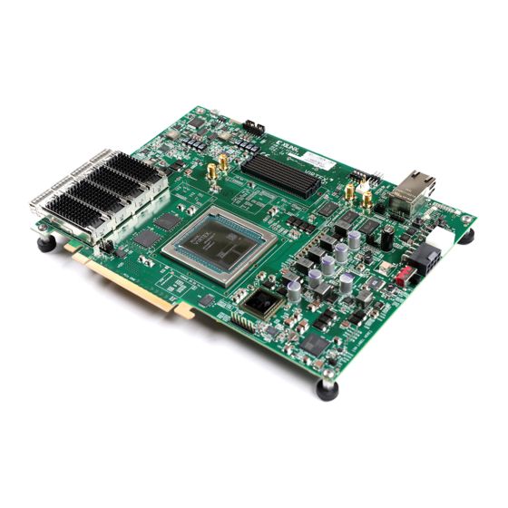
[Figure 2, callout 1] The VCU128 board incorporates the VU37P high bandwidth memory (HBM) FPGA, which utilizes stacked silicon interconnect (SSI) technology to add HBM die next to the FPGA die on the package substrate. The VCU128 board is populated with the Virtex ®... - Page 19 There are 12 I/O banks and 2 high-bandwidth memory (HBM) banks available on the XCVU37P device. The VCU128 board does not use the HBM banks. The voltages applied to the FPGA I/O banks on the VCU128 board are listed in the following table.
- Page 20 DDR4-2666 ○ The VCU128 XCVU37P FPGA DDR4 interface performance is documented in the Virtex UltraScale+ FPGA Data Sheet: DC and AC Switching Characteristics (DS923). The 72-bit wide DDR4 memory system is connected to XCVU37P U1 HP banks 64, 65 and 66.
- Page 21 POD12_DCI BH46 PL_DDR4_DQS2_T DIFF_POD12_DCI LDQS_T BJ46 PL_DDR4_DQS2_C DIFF_POD12_DCI LDQS_C BH42 PL_DDR4_DM2_B POD12_DCI NF/LDM_B/LDBI_B BE43 PL_DDR4_DQ24 POD12_DCI BF42 PL_DDR4_DQ25 POD12_DCI BC42 PL_DDR4_DQ26 POD12_DCI BF43 PL_DDR4_DQ27 POD12_DCI BD42 PL_DDR4_DQ28 POD12_DCI UG1302 (v1.0) December 21, 2018 www.xilinx.com Send Feedback VCU128 Board User Guide...
- Page 22 BH35 PL_DDR4_DQ51 POD12_DCI DQ11 BJ33 PL_DDR4_DQ52 POD12_DCI DQ12 BF35 PL_DDR4_DQ53 POD12_DCI DQ13 BG34 PL_DDR4_DQ54 POD12_DCI DQ14 BF36 PL_DDR4_DQ55 POD12_DCI DQ15 BK34 PL_DDR4_DQS6_T DIFF_POD12_DCI UDQS_T BK35 PL_DDR4_DQS6_C DIFF_POD12_DCI UDQS_C UG1302 (v1.0) December 21, 2018 www.xilinx.com Send Feedback VCU128 Board User Guide...
- Page 23 U17-U19 U73-U74 BG47 PL_DDR4_A9 SSTL12_DCI U17-U19 U73-U74 BF47 PL_DDR4_A10 SSTL12_DCI A10/AP U17-U19 U73-U74 BG49 PL_DDR4_A11 SSTL12_DCI U17-U19 U73-U74 BF48 PL_DDR4_A12 SSTL12_DCI A12/BC_B U17-U19 U73-U74 BF52 PL_DDR4_A13 SSTL12_DCI U17-U19 U73-U74 UG1302 (v1.0) December 21, 2018 www.xilinx.com Send Feedback VCU128 Board User Guide...
- Page 24 The VCU128 DDR4 memory component interfaces adhere to the constraints guidelines documented in the “DDR3/DDR4 Design Guidelines” section of the UltraScale Architecture-Based FPGAs Memory IP LogiCORE IP Product Guide (PG150). The VCU128 board DDR4 memory component interface is a 40Ω impedance implementation.
- Page 25 Up to RL3-1866 ○ The VCU128 XCVU37P FPGA RLDRAM3 interface performance is documented in the Virtex UltraScale+ FPGA Data Sheet: DC and AC Switching Characteristics (DS923). This memory system is connected to the XCVU37P HP banks 73, 74, and 75. The RLD3 0.6V VTT termination voltage (net RLD3_VTERM_0V6) is sourced from TI TPS51200DR linear regulator U92.
- Page 26 DQ18 RLD3_72B_DQ55 SSTL12 DQ19 RLD3_72B_DQ56 SSTL12 DQ20 RLD3_72B_DQ57 SSTL12 DQ21 RLD3_72B_DQ58 SSTL12 DQ22 RLD3_72B_DQ59 SSTL12 DQ23 RLD3_72B_DQ60 SSTL12 DQ24 RLD3_72B_DQ61 SSTL12 DQ25 RLD3_72B_DQ62 SSTL12 DQ26 RLD3_72B_DQ63 SSTL12 DQ27 UG1302 (v1.0) December 21, 2018 www.xilinx.com Send Feedback VCU128 Board User Guide...
- Page 27 U37, U39 RLD3_72B_A20 SSTL12 NF_A20 U37, U39 RLD3_72B_BA0 SSTL12 U37, U39 RLD3_72B_BA1 SSTL12 U37, U39 RLD3_72B_BA2 SSTL12 U37, U39 RLD3_72B_BA3 SSTL12 U37, U39 RLD3_72B_WE_B SSTL12 WE_B U37, U39 UG1302 (v1.0) December 21, 2018 www.xilinx.com Send Feedback VCU128 Board User Guide...
- Page 28 The VCU128 RLD3 72-bit memory component interface adheres to the constraints guidelines documented in the "RLD3 Design Guidelines" section of the UltraScale Architecture-Based FPGAs Memory IP LogiCORE IP Product Guide (PG150). The VCU128 RLD3 memory component interface is a 40Ω impedance implementation.
- Page 29 Maximum operating frequency of 1066 MHz ○ The VCU128 XCVU37P FPGA QDR IV interface performance is documented in the Virtex UltraScale+ FPGA Data Sheet: DC and AC Switching Characteristics (DS923). The 72-bit wide QDR4 memory is connected to XCVU37P U1 HP banks 68, 69, and 70. The QDR4 memory interface bank VREF pins are not connected, which, coupled with an XDC set_property INTERNAL VREF constraint, invoke the INTERNAL VREF mode.
- Page 30 BJ13 QDR4_DQA26 DQA26 QDR4_DQA27 DQA27 BE10 QDR4_DQA28 DQA28 BG13 QDR4_DQA29 DQA29 BE11 QDR4_DQA30 DQA30 BF10 QDR4_DQA31 DQA31 BG12 QDR4_DQA32 DQA32 QDR4_DQA33 DQA33 BG10 QDR4_DQA34 DQA34 BF12 QDR4_DQA35 DQA35 UG1302 (v1.0) December 21, 2018 www.xilinx.com Send Feedback VCU128 Board User Guide...
- Page 31 QDR4_DQB8 DQB8 QDR4_DQB9 DQB9 QDR4_DQB10 DQB10 QDR4_DQB11 DQB11 QDR4_DQB12 DQB12 QDR4_DQB13 DQB13 QDR4_DQB14 DQB14 QDR4_DQB15 DQB15 QDR4_DQB16 DQB16 QDR4_DQB17 DQB17 QDR4_DQB18 DQB18 QDR4_DQB19 DQB19 QDR4_DQB20 DQB20 QDR4_DQB21 DQB21 UG1302 (v1.0) December 21, 2018 www.xilinx.com Send Feedback VCU128 Board User Guide...
- Page 32 QKB0_N QDR4_QKB1_P QKB1_P QDR4_QKB1_N QKB1_N QDR4_QVLDB0 QVLDB0 QDR4_QVLDB1 QVLDB1 QDR4_LDB_N LDB_N QDR4_RWB_N RWB_N R606(GND) QDR4_DINVB0 DINVB0 R602(GND) QDR4_DINVB1 DINVB1 Common QDR4_A0 QDR4_A1 QDR4_A2 QDR4_A3 QDR4_A4 QDR4_A5 QDR4_A6 QDR4_A7 UG1302 (v1.0) December 21, 2018 www.xilinx.com Send Feedback VCU128 Board User Guide...
- Page 33 Notes: Resistors to GND are 100Ω. The VCU128 QDR-IV dual independent 36-bit bidirectional data port memory component interfaces adhere to the constraints guidelines documented in the "QDR-IV Design Guidelines" section of the UltraScale Architecture-Based FPGAs Memory IP LogiCORE IP Product Guide (PG150).
- Page 34 [Figure 2, callout 7] VCU128 boards host a Micron MT25QU02GCBB8E12-0SIT serial NOR flash Quad SPI flash memory capable of holding the boot image for the XCVU37P FPGA. This interface supports the QSPI32 boot mode as defined in the UltraScale Architecture Configuration User Guide (UG570).
- Page 35 2, callout 24] JTAG configuration is provided through a dual-function FTDI FT4232HL USB-to-JTAG/UART bridge device (U8) where a host computer accesses the VCU128 board JTAG chain through a type-A (PC host side) to micro-AB (VCU128 board side J2) USB cable.
- Page 36 X21649-110618 FMCP Connector JTAG Bypass When an FMC is attached to the VCU128 board FMC+ HSPC connector J18, it is automatically added to the JTAG chain through the electronically controlled single-pole single-throw (SPST) switch U72. The SPST switch is in a normally closed state and transitions to an open state when the FMC is attached.
- Page 37 USB UART Interface [Figure 2, callout 24] The FT4232HL U8 multi-function USB-UART on the VCU128 board provides three level-shifted UART connections through the single micro-AB USB connector J2. • Channel A is configured in JTAG mode to support the JTAG chain •...
- Page 38 Chapter 3: Board Component Descriptions Clock Generation [Figure 2, callout 10-18] The VCU128 evaluation board clock sources to the FPGA are listed in the following table. Table 10: Board Clock Sources Clock Name Clock Ref. Des. Description Memory Interface Clocks DDR4 clock 100 MHz SiTime SiT9120AI 3.3V fixed frequency...
- Page 39 SI5328B/U87.34 SI5328_CLOCK2_P Notes: Series capacitor coupled, MGT connections I/O standard is not applicable. Signal amplitude not to exceed FPGA U1 bank 67 VCCO = VCC1V8 rail = 1.8V. UG1302 (v1.0) December 21, 2018 www.xilinx.com Send Feedback VCU128 Board User Guide...
- Page 40 [Figure 2, callout 10] The VCU128 evaluation board has a SiTime 100 MHz fixed frequency low-jitter 3.3V LVDS differential oscillator (U76) connected to FPGA U1 HP bank 66 DDR4 interface GC pins BH51 (P) and BJ51 (N) and is series capacitor coupled.
- Page 41 [Figure 2, callout 12] The VCU128 evaluation board has a SiTime 100 MHz fixed frequency low-jitter 3.3V LVDS differential oscillator (U96) connected to FPGA U1 HP bank 69 QDR4 interface GC pins BJ4 (P) and BK3 (N) and is series capacitor coupled.
- Page 42 [Figure 2, callout 11] The VCU128 evaluation board has a SiTime 100 MHz fixed frequency low-jitter 3.3V LVDS differential oscillator (U45) connected to FPGA U1 HP bank 74 RLD3 interface GC pins F35 (P) and F36 (N) and is series capacitor coupled.
- Page 43 10 MHz to 810 MHz through an I2C interface. Power cycling the VCU128 evaluation board resets the QSFP1 clock to the default frequency of 156.250 MHz. • Programmable oscillator: Silicon Labs Si570BAB0000544DG (10 MHz-810 MHz) •...
- Page 44 10 MHz to 810 MHz through an I2C interface. Power cycling the VCU128 evaluation board resets the QSFP2 clock to the default frequency of 156.250 MHz. • Programmable oscillator: Silicon Labs Si570BAB0000544DG (10 MHz-810 MHz) •...
- Page 45 10 MHz to 810 MHz through an I2C interface. Power cycling the VCU128 evaluation board resets the QSFP3 clock to the default frequency of 156.250 MHz. • Programmable oscillator: Silicon Labs Si570BAB0000544DG (10 MHz-810 MHz) •...
- Page 46 10 MHz to 810 MHz through an I2C interface. Power cycling the VCU128 evaluation board resets the QSFP4 clock to the default frequency of 156.250 MHz • Programmable oscillator: Silicon Labs Si570BAB0000544DG (10 MHz-810 MHz) •...
- Page 47 [Figure 2, callout 18] The VCU128 board provides a pair of SMAs for differential user clock input into FPGA U1 GTY bank 131. The P-side SMA J24 signal SMA_REFCLK_INPUT_P is connected to FPGA U1 GTY bank 131 MGTREFCLK1P pin AA40, with the N-side SMA J26 signal SMA_REFCLK_INPUT_N connected to U1 GTY bank 131 MGTREFCLK1N pin AA41.
- Page 48 [Figure 2, callout 27] The VCU128 board provides a pair of SMAs for differential user clock I/O on FPGA U1 HP bank 67. The P-side SMA J12 net SMA_CLK_OUTPUT_P is connected to FPGA U1 HP bank 67 QBC pin BK26. The N-side SMA J13 net SMA_CLK_OUTPUT_N is connected to FPGA U1 HP bank 67 QBC pin BL25.
- Page 49 [Figure 2, callout 17] The VCU128 board includes a Silicon Labs Si5328B jitter attenuator U87 on the back side of the board. FPGA U1 bank 67 implements two QSFP RX differential clocks (QSFP1_RECCLK_P, pin BH26 and QSFP1_RECCLK_N, pin BH25, and QSFP2_RECCLK_P, pin BJ26 and QSFP2_RECCLK_N, pin BK25) for jitter attenuation.
- Page 50 GTY quads on the left side of the device and twelve GTY Quads on the right side of the device. The VCU128 board provides access to 14 of the 24 GTY Quads: • Four of the GTY Quads are wired to QSFP[1:4] Module Connectors (J42, J39, J35, J32) •...
- Page 51 • Four GTY transceivers allocated to FMCP_HSPC_DP[8:11] Quad 125 • MGTREFCLK0 – FMCP_HSPC_GBTCLK1_M2C_P/N • NC • Four GTY transceivers allocated to FMCP_HSPC_DP[4:7] Quad 124 • MGTREFCLK0 – FMCP_HSPC_GBTCLK0_M2C_P/N • NC UG1302 (v1.0) December 21, 2018 www.xilinx.com Send Feedback VCU128 Board User Guide...
- Page 52 FMCP_HSPC_DP23 FMCP_HSPC_DP3 MGTY_129_REFCLK0 MGTY_124_REFCLK0 FMCP_HSPC_GBTCLK5_M2C FMCP_HSPC_GBTCLK0_M2C MGTY_129_REFCLK1 MGTY_124_REFCLK1 X21650-092618 Right-side GTY Transceiver Connectivity The following tables list the connectivity of the ten XCVU37P FPGA U1 right-side GTY transceivers. UG1302 (v1.0) December 21, 2018 www.xilinx.com Send Feedback VCU128 Board User Guide...
- Page 53 TX4P MGTYTXN3_135 QSFP1_TX4_N TX4N MGTYRXP3_135 QSFP1_RX4_P RX4P MGTYRXN3_135 QSFP1_RX4_N RX4N MGTREFCLK0P_135 QSFP_SI570_CLOCK_P U95 SI570 I2C prog. osc. MGTREFCLK0N_135 QSFP_SI570_CLOCK_N OUT_B MGTREFCLK1P_135 MGTREFCLK1N_135 Notes: Series 0.01 μF capacitor coupled. UG1302 (v1.0) December 21, 2018 www.xilinx.com Send Feedback VCU128 Board User Guide...
- Page 54 MGTYRXN3_134 QSFP2_RX4_N RX4N MGTREFCLK0P_134 QSFP2_SI570_CLOCK_P U90 SI570 I2C prog. osc. MGTREFCLK0N_134 QSFP2_SI570_CLOCK_N OUT_B MGTREFCLK1P_134 SI5328_CLOCK1_C_P CKOUT1_P U87 SI5328B jitter atten. MGTREFCLK1N_134 SI5328_CLOCK1_C_N CKOUT1_N Notes: Series 0.01uF capacitor coupled. UG1302 (v1.0) December 21, 2018 www.xilinx.com Send Feedback VCU128 Board User Guide...
- Page 55 MGTYRXN3_132 QSFP3_RX4_N RX4N MGTREFCLK0P_132 QSFP3_SI570_CLOCK_P U82 SI570 I2C prog. osc. MGTREFCLK0N_132 QSFP3_SI570_CLOCK_N OUT_B MGTREFCLK1P_132 SI5328_CLOCK2_C_P CKOUT2_P U87 SI5328B jitter atten. MGTREFCLK1N_132 SI5328_CLOCK2_C_N CKOUT2_N Notes: Series 0.01uF capacitor coupled. UG1302 (v1.0) December 21, 2018 www.xilinx.com Send Feedback VCU128 Board User Guide...
- Page 56 MGTREFCLK0P_131 QSFP4_SI570_CLOCK_P U80 SI570 I2C prog. osc. AB43 MGTREFCLK0N_131 QSFP4_SI570_CLOCK_N OUT_B AA40 MGTREFCLK1P_131 SMA_REFCLK_INPUT_P SMA J24 (P) SMA J26 (N) AA41 MGTREFCLK1N_131 SMA_REFCLK_INPUT_N Notes: Series 0.01uF capacitor coupled. UG1302 (v1.0) December 21, 2018 www.xilinx.com Send Feedback VCU128 Board User Guide...
- Page 57 MGTYTXN3_129 FMCP_HSPC_DP23_C2M_N DP23_C2M_N AE49 MGTYRXP3_129 FMCP_HSPC_DP23_M2C_P DP23_M2C_P AE50 MGTYRXN3_129 FMCP_HSPC_DP23_M2C_N DP23_M2C_N AG40 MGTREFCLK0P_129 FMCP_HSPC_GBTCLK5_M2C_P GBTCLK5_M2C_P AG41 MGTREFCLK0N_129 FMCP_HSPC_GBTCLK5_M2C_N GBTCLK5_M2C_N AF42 MGTREFCLK1P_129 AF43 MGTREFCLK1N_129 Notes: Series 0.01uF capacitor coupled. UG1302 (v1.0) December 21, 2018 www.xilinx.com Send Feedback VCU128 Board User Guide...
- Page 58 MGTYTXN3_128 FMCP_HSPC_DP19_C2M_N DP19_C2M_N AH51 MGTYRXP3_128 FMCP_HSPC_DP19_M2C_P DP19_M2C_P AH52 MGTYRXN3_128 FMCP_HSPC_DP19_M2C_N DP19_M2C_N AJ40 MGTREFCLK0P_128 FMCP_HSPC_GBTCLK4_M2C_P GBTCLK4_M2C_P AJ41 MGTREFCLK0N_128 FMCP_HSPC_GBTCLK4_M2C_N GBTCLK4_M2C_N AH42 MGTREFCLK1P_128 AH43 MGTREFCLK1N_128 Notes: Series 0.01uF capacitor coupled. UG1302 (v1.0) December 21, 2018 www.xilinx.com Send Feedback VCU128 Board User Guide...
- Page 59 MGTYTXN3_127 FMCP_HSPC_DP15_C2M_N DP15_C2M_N AL53 MGTYRXP3_127 FMCP_HSPC_DP15_M2C_P DP15_M2C_P AL54 MGTYRXN3_127 FMCP_HSPC_DP15_M2C_N DP15_M2C_N AL40 MGTREFCLK0P_127 FMCP_HSPC_GBTCLK3_M2C_P GBTCLK3_M2C_P AL41 MGTREFCLK0N_127 FMCP_HSPC_GBTCLK3_M2C_N GBTCLK3_M2C_N AK42 MGTREFCLK1P_127 AK43 MGTREFCLK1N_127 Notes: Series 0.01uF capacitor coupled. UG1302 (v1.0) December 21, 2018 www.xilinx.com Send Feedback VCU128 Board User Guide...
- Page 60 MGTYTXN3_126 FMCP_HSPC_DP11_C2M_N DP11_C2M_N AP51 MGTYRXP3_126 FMCP_HSPC_DP11_M2C_P DP11_M2C_P AP52 MGTYRXN3_126 FMCP_HSPC_DP11_M2C_N DP11_M2C_N AN40 MGTREFCLK0P_126 FMCP_HSPC_GBTCLK2_M2C_P GBTCLK2_M2C_P AN41 MGTREFCLK0N_126 FMCP_HSPC_GBTCLK2_M2C_N1 GBTCLK2_M2C_N AM42 MGTREFCLK1P_126 AM43 MGTREFCLK1N_126 Notes: Series 0.01uF capacitor coupled. UG1302 (v1.0) December 21, 2018 www.xilinx.com Send Feedback VCU128 Board User Guide...
- Page 61 MGTYTXN3_125 FMCP_HSPC_DP7_C2M_N DP7_C2M_N AV51 MGTYRXP3_125 FMCP_HSPC_DP7_M2C_P DP7_M2C_P AV52 MGTYRXN3_125 FMCP_HSPC_DP7_M2C_N DP7_M2C_N AR40 MGTREFCLK0P_125 FMCP_HSPC_GBTCLK1_M2C_P GBTCLK1_M2C_P AR41 MGTREFCLK0N_125 FMCP_HSPC_GBTCLK1_M2C_N GBTCLK1_M2C_N AP42 MGTREFCLK1P_125 AP43 MGTREFCLK1N_125 Notes: Series 0.01uF capacitor coupled. UG1302 (v1.0) December 21, 2018 www.xilinx.com Send Feedback VCU128 Board User Guide...
- Page 62 MGTREFCLK1 - not connected ○ Four GTY transceivers allocated to PCIe lanes 3:0 PCIE_EP_TX/RX[3:0] ○ • Quad 226 MGTREFCLK0 - not connected ○ MGTREFCLK1 - not connected ○ UG1302 (v1.0) December 21, 2018 www.xilinx.com Send Feedback VCU128 Board User Guide...
- Page 63 (PG182). For additional information about the quad small form factor pluggable (28 Gb/s QSFP28) module, see the SFF-8663 and SFF-8679 specifications for the 28 Gb/s QSFP+ at the SNIA Technology Affiliates website. UG1302 (v1.0) December 21, 2018 www.xilinx.com Send Feedback VCU128 Board User Guide...
- Page 64 MGTYTXN3_227 PCIE_EP_TX0_N PERN0 MGTYRXP3_227 PCIE_EP_RX0_P PETP0 MGTYRXN3_227 PCIE_EP_RX0_N PETN0 AL15 MGTREFCLK0P_227 PCIE_CLK2_P ICS85411A U94 clock AL14 MGTREFCLK0N_227 PCIE_CLK2_N buffer AK13 MGTREFCLK1P_227 AK12 MGTREFCLK1N_227 Notes: Series 0.01uF capacitor coupled. UG1302 (v1.0) December 21, 2018 www.xilinx.com Send Feedback VCU128 Board User Guide...
- Page 65 PETN5 AR11 MGTYTXP3_226 PCIE_EP_TX4_P PERP4 AR10 MGTYTXN3_226 PCIE_EP_TX4_N PERN4 MGTYRXP3_226 PCIE_EP_RX4_P PETP4 MGTYRXN3_226 PCIE_EP_RX4_N PETN4 AN15 MGTREFCLK0P_226 AN14 MGTREFCLK0N_226 AM13 MGTREFCLK1P_226 AM12 MGTREFCLK1N_226 Notes: Series 0.01uF capacitor coupled. UG1302 (v1.0) December 21, 2018 www.xilinx.com Send Feedback VCU128 Board User Guide...
- Page 66 MGTYTXN3_225 PCIE_EP_TX8_N PERN8 MGTYRXP3_225 PCIE_EP_RX8_P PETP8 MGTYRXN3_225 PCIE_EP_RX8_N PETN8 AR15 MGTREFCLK0P_225 PCIE_CLK1_P ICS85411A U94 clock AR14 MGTREFCLK0N_225 PCIE_CLK1_N buffer AP13 MGTREFCLK1P_225 AP12 MGTREFCLK1N_225 Notes: Series 0.01uF capacitor coupled. UG1302 (v1.0) December 21, 2018 www.xilinx.com Send Feedback VCU128 Board User Guide...
- Page 67 Gen4 applications. The PCIe transmit and receive signal data paths have a characteristic impedance of 85Ω ±10%. The PCIe clock is routed as a 100Ω differential pair. UG1302 (v1.0) December 21, 2018 www.xilinx.com Send Feedback VCU128 Board User Guide...
- Page 68 Chapter 3: Board Component Descriptions The XCVU37P-2FSVH2892E (-2 speed grade) is deployed on the VCU128 to support up to Gen4 x8. User selectable as PCIe Gen3 x16 or dual Gen4 x8. The PCIe reference clock is input from the P1 edge connector. The PCIe clock is routed from P1 pin A16 (P) and pin A17 (N) to a 1-to-2 ICS85411A clock buffer U94.
- Page 69 [Figure 2, callout 19] The VCU128 board hosts four QSFP28 small form-factor pluggable (28 Gb/s QSFP+) connectors: QSFP1 J42, QSFP2 J39, QSFP3 J35, and QSFP4 J32, which accept 28 Gb/s QSFP+ optical modules. The four connectors are housed within a single 1x4 ganged 28 Gb/s QSFP+ cage assembly J37.
- Page 70 QSFP4 J32 (U1 bank 67) BK23 QSFP4_MODSKLL_LS Output MODSELL BK24 QSFP4_RESETL_LS Output RESETL BL22 QSFP4_MODPRSL_LS Output MODPRSL BH21 QSFP4_INTL_LS Input INTL BH21 QSFP4_LPMODE_LS Output LPMODE U54.19 QSFP4_I2C_SDA BiDir UG1302 (v1.0) December 21, 2018 www.xilinx.com Send Feedback VCU128 Board User Guide...
- Page 71 [Figure 2, callout 22] The VCU128 evaluation board uses the TI PHY device DP83867ISRGZ (U62) for Ethernet communications at 10 Mb/s, 100 Mb/s, or 1000 Mb/s. The board supports SGMII mode only. The PHY connection to a user-provided Ethernet cable is through RJ-45 connector P2, a Wurth 7499111221A with built-in magnetics and status LEDs.
- Page 72 Two Ethernet PHY status LEDs are integrated into the metal frame of the P2 RJ-45 connector, installed on the top edge and towards the back of the VCU128 board. The two PHY status LEDs are visible within the frame of the RJ45 Ethernet jack as shown in the following figure. As viewed from the front opening, the left green LED is the link activity indicator and the right green LED is the 1000BASE-T link mode indicator.
- Page 73 I2C0 U55 PCA9544A, address 0x75 (0b111101); U53 TCA9548A, address 0x74 (0b1110100), or U54 TCA9548A, address 0x76 (0b111110), respectively. The following table lists the address for each bus. UG1302 (v1.0) December 21, 2018 www.xilinx.com Send Feedback VCU128 Board User Guide...
- Page 74 0b1010000 0x50 QSFP4 module J32 28 Gb/s QSFP+ 0b1010000 0x50 Notes: Onboard Power System Devices. Information about the PCA9544A, TCA9548, and TCA6416A is available on the Semiconductor website. UG1302 (v1.0) December 21, 2018 www.xilinx.com Send Feedback VCU128 Board User Guide...
- Page 75 Chapter 3: Board Component Descriptions Status and User LEDs [Figure 2, callout 24] The following table defines VCU128 board status and user LEDs. Table 29: Board Status and User LEDs Description Reference Designator (Green unless otherwise noted) Combined power good (red/green)
- Page 76 Chapter 3: Board Component Descriptions User GPIO [Figure 2, callout 27, 28, 29] The VCU128 board provides the following user and general purpose I/O capabilities. • Eight user LEDs (callout 28) GPIO_LED[7-0]: DS9, DS8, DS7, DS6, DS5, DS4, DS3, DS2 ○...
- Page 77 12VDC power from the 6-pin mini-fit power input connector J16, normally used in bench-top applications with the provided power adapter. The green LED DS20 illuminates when the VCU128 board power switch is on. See Board Power System for details on the onboard power system.
- Page 78 Chapter 3: Board Component Descriptions Power On/Off Switch SW5 Figure 27: X21973-112818 When the VCU128 board is used inside a computer chassis (i.e., plugged in to a PCIe ® slot), power is normally provided from the PC ATX supply 2x4 PCIe power connector. See...
- Page 79 24. Also, there is an optional extension connector (the high serial pin connector extension, or HSPCe) to boost pin-count by 80 positions, arranged in a 4x20 array. The VCU128 board does not implement the high serial pin connector/HSPCe extension.
- Page 80 • 68 single-ended or 34 differential user-defined pairs (full LA-bus: LA[00:33]) • 24 transceiver differential pairs • 6 transceiver differential clocks • 2 differential clocks • 239 ground and 14 power connections UG1302 (v1.0) December 21, 2018 www.xilinx.com Send Feedback VCU128 Board User Guide...
- Page 81 AU49 FMCP_HSPC_DP3_C2M_N LVDS BA45 FMCP_HSPC_DP7_C2M_P LVDS AU44 FMCP_HSPC_DP4_C2M_P LVDS AY46 FMCP_HSPC_DP7_C2M_N LVDS AU45 FMCP_HSPC_DP4_C2M_N LVDS AY47 FMCP_HSPC_DP6_C2M_P LVDS AV46 FMCP_HSPC_DP5_C2M_P LVDS AW44 FMCP_HSPC_DP6_C2M_N LVDS AV47 FMCP_HSPC_DP5_C2M_N LVDS AW45 UG1302 (v1.0) December 21, 2018 www.xilinx.com Send Feedback VCU128 Board User Guide...
- Page 82 FMCP_HSPC_LA23_N LVDS FMCP_HSPC_IIC_SDA FMCP_HSPC_LA26_P LVDS GA0 = 0 = GND FMCP_HSPC_LA26_N LVDS VCC12_SW FMCP_HSPC_TCK_BUF VCC12_SW FPGA_TDO_FMC_TDI_BUF UTIL_3V3 FMCP_HSPC_TDO_HPC1_TDI UTIL_3V3 FMCP_HSPC_TMS_BUF GA1 = 0 = GND UTIL_3V3 UTIL_3V3 UTIL_3V3 UG1302 (v1.0) December 21, 2018 www.xilinx.com Send Feedback VCU128 Board User Guide...
- Page 83 FMCP_HSPC_LA24_P LVDS FMCP_HSPC_LA29_N LVDS FMCP_HSPC_LA24_N LVDS FMCP_HSPC_LA31_P LVDS FMCP_HSPC_LA28_P LVDS FMCP_HSPC_LA31_N LVDS FMCP_HSPC_LA28_N LVDS FMCP_HSPC_LA33_P LVDS FMCP_HSPC_LA30_P LVDS FMCP_HSPC_LA33_N LVDS FMCP_HSPC_LA30_N LVDS VADJ_1V8_FPGA FMCP_HSPC_LA32_P LVDS FMCP_HSPC_LA32_N LVDS VADJ UG1302 (v1.0) December 21, 2018 www.xilinx.com Send Feedback VCU128 Board User Guide...
- Page 84 FMCP_HSPC_SYNC_M2C_P LVDS FMCP_HSPC_DP16_C2M_N LVDS AK47 FMCP_HSPC_SYNC_M2C_N LVDS FMCP_HSPC_DP17_C2M_P LVDS AJ48 FMCP_HSPC_DP17_C2M_N LVDS AJ49 FMCP_HSPC_DP18_C2M_P LVDS AJ44 VCC12_SW FMCP_HSPC_DP18_C2M_N LVDS AJ45 VCC12_SW FMCP_HSPC_DP19_C2M_P LVDS AH46 VCC12_SW FMCP_HSPC_DP19_C2M_N LVDS AH47 UG1302 (v1.0) December 21, 2018 www.xilinx.com Send Feedback VCU128 Board User Guide...
- Page 85 Marketing Alliance website. Board Power System [Figure 2, callout 34] The VCU128 board has an Intersil power system. The following figure shows the VCU128 board power system block diagram. UG1302 (v1.0) December 21, 2018 www.xilinx.com Send Feedback VCU128 Board User Guide...
- Page 86 1.2V @ 20A ISL68301 + ISL919227B 103W Current Shunt VCCINT 0.85V @ 125A ISL68127 + ISL919227 (5) Current Shunt VCCBRAM 0.85V @ 30A ISL68127 + ISL919227 (1) X21654-121718 UG1302 (v1.0) December 21, 2018 www.xilinx.com Send Feedback VCU128 Board User Guide...
- Page 87 Chapter 3: Board Component Descriptions Onboard Power System Devices The VCU128 evaluation board uses programmable power regulators from Intersil Corporation to supply the core and auxiliary voltages listed in the following table. Table 32: Onboard Power System Devices INA226 Iout...
- Page 88 • If no FMC card is attached to the FMC port, the VADJ voltage is set to 0V • When an FMC card is attached, its IIC EEPROM is read to find a VADJ voltage supported by both the VCU128 board and the FMC module, within the available choices of 1.2V, 1.5V, 1.8V, and 0.0V •...
- Page 89 Jumper selectable at 3-pin header J25: 1-2 = 0.85V (default); 2-3 = 0.72V Cooling Fan The XCVU37P FPGA U1 cooling fan connector is shown in the following figure. The VCU128 fan circuit uses a Maxim MAX6643 fan controller that autonomously monitors the FPGA die temperature pins DXP and DXN.
- Page 90 The VCU128 board includes an onboard Zynq -7000 SoC U42 as the system controller. A host PC resident graphical user interface for the system controller (SCUI) is provided on the VCU128 website. The SCUI can be used to query and control select programmable features such as clocks, FMC functionality, and power systems.
- Page 91 Chapter 3: Board Component Descriptions X21976-112818 See the VCU128 System Controller Tutorial (XTP534) and the VCU128 Software Install and Board Setup Tutorial (XTP535) for more information on installing and using the System Controller utility. Configuration Options [Figure 2, callout 36] The VCU128 board supports two of the seven UltraScale™...
- Page 92 FPGA. DIP switch SW1 also includes a system controller enable switch in position 1. See the UltraScale Architecture Configuration User Guide (UG570) for further details on configuration modes. UG1302 (v1.0) December 21, 2018 www.xilinx.com Send Feedback VCU128 Board User Guide...
-
Page 93: Appendix A: Vita 57.4 Fmcp Connector Pinouts
Overview The following figure shows the pinout of the FPGA mezzanine card plus (FMCP) connector J18 defined by the VITA 57.4 FMC specification. For a description of how the VCU128 evaluation board implements the FMCP specification, see FPGA Mezzanine Card Interface. -
Page 94: Appendix B: Xilinx Constraints File
® design constraints (XDC) file template for the VCU128 board provides for designs targeting the VCU128 evaluation board. Net names in the constraints listed correlate with net names on the latest VCU128 evaluation board schematic. Identify the appropriate pins and replace the net names with the net names in the user RTL. -
Page 95: Appendix C: Regulatory And Compliance Information
Regulatory and Compliance Information Overview This product is designed and tested to conform to the European Union directives and standards described in this section. VCU128 Evaluation Kit - Master Answer Record 71849 For Technical Support, open a Support Service Request. CE Directives... -
Page 96: Compliance Markings
Xilinx has met its national obligations to the EU WEEE Directive by registering in those countries to which Xilinx is an importer. Xilinx has also elected to join WEEE Compliance Schemes in some countries to help manage customer returns at end-of-life. -
Page 97: Appendix D: Additional Resources And Legal Notices
• On Windows, select Start → All Programs → Xilinx Design Tools → DocNav. • At the Linux command prompt, enter docnav. Xilinx Design Hubs provide links to documentation organized by design tasks and other topics, which you can use to learn key concepts and address frequently asked questions. To access the Design Hubs: •... - Page 98 Appendix D: Additional Resources and Legal Notices References The most up to date information related to the VCU128 board and its documentation is available on the following websites. VCU128 Evaluation Kit VCU128 Evaluation Kit - Master Answer Record 71849 These documents provide supplemental material useful with this guide: 1.
- Page 99 ATX Power Supply Adapter Cable The Xilinx ATX cable part number 2600304 is manufactured by Sourcegate Technologies and is equivalent to the Sourcegate Technologies part number AZCBL-WH-11009. Sourcegate only manufactures the latest revision, which is currently A4. To order, contact Aries Ang, aries.ang@sourcegate.net, +65 6483 2878 for price and availability.
- Page 100 IP cores may be subject to warranty and support terms contained in a license issued to you by Xilinx. Xilinx products are not designed or intended to be fail-safe or for use in any application requiring fail-safe performance; you assume sole risk and liability for...
Need help?
Do you have a question about the VCU128 and is the answer not in the manual?
Questions and answers