Table of Contents
Advertisement
Quick Links
Advertisement
Table of Contents

Subscribe to Our Youtube Channel
Related Manuals for Alinx Z19


Summary of Contents for Alinx Z19
- Page 1 Z19 User Manual Zynq UltraScale+ MPSoC Development Board User Manual...
-
Page 2: Table Of Contents
Z19 User Manual Table of Contents Table of Contents ..............................2 1. FPGA Development Board Introduction ....................... 6 2. ZYNQ Chip Introduction ............................. 9 3. DDR4 DRAM ................................. 11 4. QSPI Flash ................................23 5. eMMC Flash ................................25 6. Clock Configuration ............................26 7. - Page 3 Z19 User Manual 22. JTAG Debugging Interface ..........................69 23. RTC Real-time Clock ............................69 24. EEPROM and Temperature Sensor ......................70 25. LED Light ................................71 26. Keys ..................................71 27. Dip Switch Configuration ..........................72 28. Fan ..................................73 29.
- Page 4 Z19 User Manual Based on XILINX Zynq UltraScale+MPSoCs development platform, our company's development board 2021 (Model: Z19) has officially released, and we have prepared this user manual for your quick understanding of this development platform. This MPSoCs FPGA development platform uses the solution of ZU19EG, a XILINX Zynq...
- Page 5 Z19 User Manual www.alinx.com...
-
Page 6: Fpga Development Board Introduction
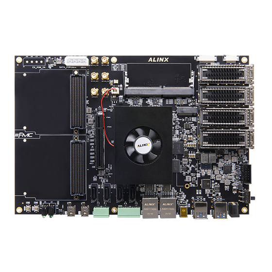
Z19 User Manual 1. FPGA Development Board Introduction The Z19 MPSoCs is mainly composed of ZU19EG, 4 DDR4, DDR4 SODIMM, eMMC, and 2 QSPI FLASH. Its main chip adopts Xilinx's Zynq UltraScale+ MPSoCs series chip, model XCZU19EG--2FFVC1760I. The ZU19EG chip can be divided into a Processor System part (PS) and a Programmable Logic part (PL), and 4 pieces of DDR4 and one 260-pin DDR4 SODIMM slot are attached to the two sides respectively. - Page 7 Z19 User Manual With this diagram, we can see the interfaces and functions that our development platform contains. ⚫ Xilinx ARM+FPGA chip XCZU19EG -- 2FFVC1760I ⚫ DDR4 Four large-capacity 2GB (8GB in total) high-speed DDR4 SDRAM chips on the PS side.
- Page 8 Z19 User Manual Four USB3.0 HOST interfaces of TYPE A are used to connect external USB peripherals, such as mouse, keyboard, U disk and others. ⚫ Gigabit Ethernet interface Two 10/100M/1000M Ethernet RJ45 interfaces, one each for PS and PL, for Ethernet data exchange with computers or other network devices.
-
Page 9: Zynq Chip Introduction
Z19 User Manual ⚫ MIPI interface Two LANE MIPI camera input interfaces for connecting to the MIPI camera module (AN5641). ⚫ JTAG Debugging interface One 10-pin 2.54mm standard JTAG interface for FPGA program download and debugging. Users can debug and download ZU9EG system through XILINX downloader. - Page 10 Z19 User Manual The ZU19EG chip supports 32-bit or 64-bit DDR4, LPDDR4, DDR3, DDR3L, LPDDR3 memory chips, and has rich high-speed interfaces on the PS side, such as PCIE Gen2, USB3.0, SATA 3.1, and DisplayPort. It also supports USB2.0, Gigabit Ethernet, SD/SDIO, I2C, CAN, UART, GPIO and other interfaces.
-
Page 11: Ddr4 Dram
FFVC1760. 3. DDR4 DRAM The Z19 development board is equipped with four Micron 2GB DDR4 chips (model MT40A1G16KD-062E), which are all mounted on the PS side, comprising a 64-bit data bus bandwidth and 8GB capacity, while a 260-pin DDR4 SODIMM slot is led on the PL side. - Page 12 Z19 User Manual Bit Number Chip Model Capacity Manufacturer U4,U5,U6,U7 MT40A1G16KD-062E 1G x 16bit Micron Table 2-3-1: DDR4 SDRAM Configuration The hardware design of DDR4 requires strict consideration of signal integrity, so we have fully considered the matching resistance/terminal resistance, trace impedance control, and trace length control in circuit design and PCB design to ensure high-speed and stable operation of DDR4.
- Page 13 Z19 User Manual PS Side DDR4 DRAM pin assignment: Signal Name Pin Name Pin Number PS_DDR4_DQS0_N PS_DDR_DQS_N0_504 BA30 PS_DDR4_DQS0_P PS_DDR_DQS_P0_504 AY30 PS_DDR4_DQS1_N PS_DDR_DQS_N1_504 AY33 PS_DDR4_DQS1_P PS_DDR_DQS_P1_504 AY32 PS_DDR4_DQS2_N PS_DDR_DQS_N2_504 AT30 PS_DDR4_DQS2_P PS_DDR_DQS_P2_504 AR30 PS_DDR4_DQS3_N PS_DDR_DQS_N3_504 AT32 PS_DDR4_DQS3_P PS_DDR_DQS_P3_504 AR32 PS_DDR4_DQS4_N...
- Page 14 Z19 User Manual PS_DDR4_DQ7 PS_DDR_DQ7_504 BA31 PS_DDR4_DQ8 PS_DDR_DQ8_504 BB33 PS_DDR4_DQ9 PS_DDR_DQ9_504 BA32 PS_DDR4_DQ10 PS_DDR_DQ10_504 BA33 PS_DDR4_DQ11 PS_DDR_DQ11_504 BB34 PS_DDR4_DQ12 PS_DDR_DQ12_504 AV31 PS_DDR4_DQ13 PS_DDR_DQ13_504 AW32 PS_DDR4_DQ14 PS_DDR_DQ14_504 AV32 PS_DDR4_DQ15 PS_DDR_DQ15_504 AV33 PS_DDR4_DQ16 PS_DDR_DQ16_504 AN29 PS_DDR4_DQ17 PS_DDR_DQ17_504 AP29 PS_DDR4_DQ18 PS_DDR_DQ18_504 AP30 PS_DDR4_DQ19...
- Page 15 Z19 User Manual PS_DDR4_DQ32 PS_DDR_DQ32_504 AN41 PS_DDR4_DQ33 PS_DDR_DQ33_504 AN42 PS_DDR4_DQ34 PS_DDR_DQ34_504 AP42 PS_DDR4_DQ35 PS_DDR_DQ35_504 AP41 PS_DDR4_DQ36 PS_DDR_DQ36_504 AN39 PS_DDR4_DQ37 PS_DDR_DQ37_504 AR38 PS_DDR4_DQ38 PS_DDR_DQ38_504 AP39 PS_DDR4_DQ39 PS_DDR_DQ39_504 AN38 PS_DDR4_DQ40 PS_DDR_DQ40_504 AL37 PS_DDR4_DQ41 PS_DDR_DQ41_504 AL38 PS_DDR4_DQ42 PS_DDR_DQ42_504 AK38 PS_DDR4_DQ43 PS_DDR_DQ43_504 AK39 PS_DDR4_DQ44...
- Page 16 Z19 User Manual PS_DDR4_DQ57 PS_DDR_DQ57_504 AM38 PS_DDR4_DQ58 PS_DDR_DQ58_504 AM40 PS_DDR4_DQ59 PS_DDR_DQ59_504 AM41 PS_DDR4_DQ60 PS_DDR_DQ60_504 AJ42 PS_DDR4_DQ61 PS_DDR_DQ61_504 AK42 PS_DDR4_DQ62 PS_DDR_DQ62_504 AK40 PS_DDR4_DQ63 PS_DDR_DQ63_504 AK41 PS_DDR4_DM0 PS_DDR_DM0_504 AY29 PS_DDR4_DM1 PS_DDR_DM1_504 AY34 PS_DDR4_DM2 PS_DDR_DM2_504 AR29 PS_DDR4_DM3 PS_DDR_DM3_504 AR33 PS_DDR4_DM4 PS_DDR_DM4_504 AR39 PS_DDR4_DM5...
- Page 17 Z19 User Manual PS_DDR4_A10 PS_DDR_A10_504 AU35 PS_DDR4_A11 PS_DDR_A11_504 AU36 PS_DDR4_A12 PS_DDR_A12_504 AW36 PS_DDR4_A13 PS_DDR_A13_504 AW37 PS_DDR4_ACT_B PS_DDR_ACT_N_504 AR37 PS_DDR4_ALERT_B PS_DDR_ALERT_N_504 AM36 PS_DDR4_BA0 PS_DDR_BA0_504 AN37 PS_DDR4_BA1 PS_DDR_BA1_504 AN36 PS_DDR4_BG0 PS_DDR_BG0_504 AP36 PS_DDR4_CAS_B PS_DDR_A15_504 AW34 PS_DDR4_CKE0 PS_DDR_CKE0_504 AY38 PS_DDR4_CLK0_N PS_DDR_CK_N0_504 BA37 PS_DDR4_CLK0_P...
- Page 18 Z19 User Manual PL_DDR4_DQS1_P IO_L10P_T1U_N6_QBC_AD4P_71 PL_DDR4_DQS2_N IO_L16N_T2U_N7_QBC_AD3N_71 PL_DDR4_DQS2_P IO_L16P_T2U_N6_QBC_AD3P_71 PL_DDR4_DQS3_N IO_L22N_T3U_N7_DBC_AD0N_71 PL_DDR4_DQS3_P IO_L22P_T3U_N6_DBC_AD0P_71 PL_DDR4_DQS4_N IO_L4N_T0U_N7_DBC_AD7N_69 PL_DDR4_DQS4_P IO_L4P_T0U_N6_DBC_AD7P_69 PL_DDR4_DQS5_N IO_L10N_T1U_N7_QBC_AD4N_69 PL_DDR4_DQS5_P IO_L10P_T1U_N6_QBC_AD4P_69 PL_DDR4_DQS6_N IO_L16N_T2U_N7_QBC_AD3N_69 PL_DDR4_DQS6_P IO_L16P_T2U_N6_QBC_AD3P_69 PL_DDR4_DQS7_N IO_L22N_T3U_N7_DBC_AD0N_69 PL_DDR4_DQS7_P IO_L22P_T3U_N6_DBC_AD0P_69 PL_DDR4_DQ0 IO_L3P_T0L_N4_AD15P_71 PL_DDR4_DQ1 IO_L3N_T0L_N5_AD15N_71 PL_DDR4_DQ2 IO_L6P_T0U_N10_AD6P_71 PL_DDR4_DQ3 IO_L5P_T0U_N8_AD14P_71 PL_DDR4_DQ4 IO_L2N_T0L_N3_71 PL_DDR4_DQ5...
- Page 19 Z19 User Manual PL_DDR4_DQ12 IO_L11N_T1U_N9_GC_71 PL_DDR4_DQ13 IO_L12N_T1U_N11_GC_71 PL_DDR4_DQ14 IO_L9P_T1L_N4_AD12P_71 PL_DDR4_DQ15 IO_L9N_T1L_N5_AD12N_71 PL_DDR4_DQ16 IO_L17N_T2U_N9_AD10N_71 PL_DDR4_DQ17 IO_L17P_T2U_N8_AD10P_71 PL_DDR4_DQ18 IO_L14P_T2L_N2_GC_71 PL_DDR4_DQ19 IO_L18N_T2U_N11_AD2N_71 PL_DDR4_DQ20 IO_L15N_T2L_N5_AD11N_71 PL_DDR4_DQ21 IO_L15P_T2L_N4_AD11P_71 PL_DDR4_DQ22 IO_L18P_T2U_N10_AD2P_71 PL_DDR4_DQ23 IO_L14N_T2L_N3_GC_71 PL_DDR4_DQ24 IO_L20N_T3L_N3_AD1N_71 PL_DDR4_DQ25 IO_L21P_T3L_N4_AD8P_71 PL_DDR4_DQ26 IO_L24P_T3U_N10_71 PL_DDR4_DQ27 IO_L24N_T3U_N11_71 PL_DDR4_DQ28 IO_L20P_T3L_N2_AD1P_71 PL_DDR4_DQ29 IO_L21N_T3L_N5_AD8N_71 PL_DDR4_DQ30...
- Page 20 Z19 User Manual PL_DDR4_DQ37 IO_L6N_T0U_N11_AD6N_69 PL_DDR4_DQ38 IO_L3P_T0L_N4_AD15P_69 PL_DDR4_DQ39 IO_L3N_T0L_N5_AD15N_69 PL_DDR4_DQ40 IO_L9N_T1L_N5_AD12N_69 PL_DDR4_DQ41 IO_L8N_T1L_N3_AD5N_69 PL_DDR4_DQ42 IO_L11N_T1U_N9_GC_69 PL_DDR4_DQ43 IO_L11P_T1U_N8_GC_69 PL_DDR4_DQ44 IO_L9P_T1L_N4_AD12P_69 PL_DDR4_DQ45 IO_L8P_T1L_N2_AD5P_69 PL_DDR4_DQ46 IO_L12P_T1U_N10_GC_69 PL_DDR4_DQ47 IO_L12N_T1U_N11_GC_69 PL_DDR4_DQ48 IO_L15N_T2L_N5_AD11N_69 PL_DDR4_DQ49 IO_L18N_T2U_N11_AD2N_69 PL_DDR4_DQ50 IO_L14N_T2L_N3_GC_69 PL_DDR4_DQ51 IO_L15P_T2L_N4_AD11P_69 PL_DDR4_DQ52 IO_L18P_T2U_N10_AD2P_69 PL_DDR4_DQ53 IO_L14P_T2L_N2_GC_69 PL_DDR4_DQ54 IO_L17P_T2U_N8_AD10P_69 PL_DDR4_DQ55...
- Page 21 Z19 User Manual PL_DDR4_DQ62 IO_L24N_T3U_N11_69 PL_DDR4_DQ63 IO_L23N_T3U_N9_69 PL_DDR4_DQ64 IO_L24P_T3U_N10_70 PL_DDR4_DQ65 IO_L21P_T3L_N4_AD8P_70 PL_DDR4_DQ66 IO_L23N_T3U_N9_70 PL_DDR4_DQ67 IO_L20P_T3L_N2_AD1P_70 PL_DDR4_DQ68 IO_L23P_T3U_N8_70 PL_DDR4_DQ69 IO_L24N_T3U_N11_70 PL_DDR4_DQ70 IO_L21N_T3L_N5_AD8N_70 PL_DDR4_DQ71 IO_L20N_T3L_N3_AD1N_70 PL_DDR4_DM0 IO_L1P_T0L_N0_DBC_71 PL_DDR4_DM1 IO_L7P_T1L_N0_QBC_AD13P_71 PL_DDR4_DM2 IO_L13P_T2L_N0_GC_QBC_71 PL_DDR4_DM3 IO_L19P_T3L_N0_DBC_AD9P_71 PL_DDR4_DM4 IO_L1P_T0L_N0_DBC_69 PL_DDR4_DM5 IO_L7P_T1L_N0_QBC_AD13P_69 PL_DDR4_DM6 IO_L13P_T2L_N0_GC_QBC_69 PL_DDR4_DM7 IO_L19P_T3L_N0_DBC_AD9P_69 PL_DDR4_DM8...
- Page 22 Z19 User Manual PL_DDR4_A6 IO_L4N_T0U_N7_DBC_AD7N_70 PL_DDR4_A7 IO_L18N_T2U_N11_AD2N_70 PL_DDR4_A8 IO_L9N_T1L_N5_AD12N_70 PL_DDR4_A9 IO_L10N_T1U_N7_QBC_AD4N_70 PL_DDR4_A10 IO_L16N_T2U_N7_QBC_AD3N_70 PL_DDR4_A11 IO_L16P_T2U_N6_QBC_AD3P_70 PL_DDR4_A12 IO_L15N_T2L_N5_AD11N_70 PL_DDR4_A13 IO_L7P_T1L_N0_QBC_AD13P_70 PL_DDR4_ACT_B IO_L9P_T1L_N4_AD12P_70 PL_DDR4_ALERT_B IO_L10P_T1U_N6_QBC_AD4P_70 PL_DDR4_BA0 IO_L4P_T0U_N6_DBC_AD7P_70 PL_DDR4_BA1 IO_T1U_N12_70 PL_DDR4_BG0 IO_L17N_T2U_N9_AD10N_70 PL_DDR4_BG1 IO_L17P_T2U_N8_AD10P_70 PL_DDR4_CAS_B IO_L7N_T1L_N1_QBC_AD13N_70 PL_DDR4_CKE0 IO_L18P_T2U_N10_AD2P_70 PL_DDR4_CKE1 IO_T2U_N12_70 PL_DDR4_CLK0_N IO_L13N_T2L_N1_GC_QBC_70 PL_DDR4_CLK0_P...
-
Page 23: Qspi Flash
Z19 User Manual PL_DDR4_PARITY IO_L3P_T0L_N4_AD15P_70 PL_DDR4_RAS_B IO_L8N_T1L_N3_AD5N_70 PL_DDR4_RST IO_L15P_T2L_N4_AD11P_70 PL_DDR4_SCL IO_L9P_AD3P_93 PL_DDR4_SDA IO_L9N_AD3N_93 PL_DDR4_WE_B IO_L5N_T0U_N9_AD14N_70 4. QSPI Flash The FPGA core board ACU9EG is equipped with two 256MBit Quad-SPI FLASH chip to form an 8-bit bandwidth data bus, the flash model is... - Page 24 Z19 User Manual Figure 2-4-1: QSPI Flash in the schematic Configure chip pin assignments: Signal Name Pin Name Pin Number MIO5_QSPI0_SS_B PS_MIO5_500 AL32 MIO0_QSPI0_SCLK PS_MIO0_500 AM33 MIO4_QSPI0_IO0 PS_MIO4_500 AL33 MIO1_QSPI0_IO1 PS_MIO1_500 AM29 MIO2_QSPI0_IO2 PS_MIO2_500 AM31 MIO3_QSPI0_IO3 PS_MIO3_500 AM30 MIO7_QSPI1_SS_B PS_MIO7_500...
-
Page 25: Emmc Flash
Z19 User Manual 5.eMMC Flash Z19 is equipped with a large-capacity 8GB eMMC FLASH chip (MTFC32GAPALBH-IT), which supports the HS-MMC port of the JEDEC e-MMC V5.0 standard, and the level supports 1.8V or 3.3V. The data width of eMMC FLASH and ZYNQ connection is 8bit. -
Page 26: Clock Configuration
AG35 6.Clock Configuration Z19 provides reference clock and RTC real-time clock for PS system and PL logic respectively, so that PS system and PL logic can work independently. The schematic diagram of the clock circuit design is shown in Figure 6-1:... - Page 27 Z19 User Manual PS System RTC Real-Time Clock The passive crystal Y1 on the core board provides a 32.768KHz real-time clock source for the PS system. The crystal is connected to the pins of PS_PADI_503 and PS_PADO_503 of the BANK503 of the ZYNQ chip. Figure 6-2 shows the schematic diagram.
-
Page 28: Power Supply
FPGA. Figure 6-4 shows the schematic diagram of the clock source. Figure 6-4: PL system clock source PL Clock pin assignment: Signal Name PL_CLK0_P PL_CLK0_N 7.Power Supply The power supply voltage of the Z19 development board is +12V, and +5V, +5V_SATA, +3.3V_PCIE, +3.3V_QSFP, +1.8V power supplies generated... - Page 29 Z19 User Manual multiple-channel DCDC chip inside the board. For the ZYNQ chip's power supply, one MAX20796GFB+ power chip provides 0.85V core power supply for XCZU19EG by 60A current, and two TPS74801DRCR power chips generate 0.85V and 1.8V voltage respectively to supply power for PS_MGT part. Two MAX20812AFH+ power chips are used to generate two-channel 0.9V and two-channel 1.2V voltages respectively to...
- Page 30 Figure 7-1: The design diagram of TPS6508640 8.M.2 Port The Z19 development board is equipped with a PCIE x1 standard M.2 port for connecting to M.2 SSDS with communication speeds of up to 6Gbps. The M.2 port uses the M key slot and supports only PCI-E, but not SATA. You need to select a PCIE SSD when selecting an SSD.
-
Page 31: Port
PCIE reset signal 9.DP Display Port The Z19 development board is equipped with a mini DisplayPort output display port for video image display. The port supports VESA DisplayPort V1.2a output standard, up to 4K x 2K@30Fps output, Y-only, YCbCr444, YCbCr422, YCbCr420 and RGB video formats. -
Page 32: Usb3.0 Port
DP insertion signal detection 10.USB3.0 Port The Z19 expansion board has four USB3.0 ports, supports HOST mode, and delivers data in a transmission speed of up to 5.0Gb/s. USB3.0 is connected through the PIPE3 port, and USB2.0 is connected to the external USB3320C chip through the ULPI port to achieve high-speed data communication between USB3.0 and USB2.0. -
Page 33: Gigabit Ethernet Port
PS_MIO44_501 11.Gigabit Ethernet Port The Z19 expansion board has two Gigabit Ethernet ports, one of which is connected to the PS side and the other to the PL side. The GPHY chip uses Micrel's KSZ9031RNX Ethernet PHY chip to provide users with network communication services. The KSZ9031RNX chip supports network transmission rate of 10/100/1000 Mbps and communicates with the MAC layer of ZU9EG system through the RGMII port. - Page 34 Z19 User Manual KSZ9031RNX supports MDI/MDX self-adaptive, various speed self-adaptive, Master/Slave self-adaptive, support MDIO bus for PHY register management. KSZ9031RNX power-on will detect some specific IO level state, so as to determine its own working mode. Table 11-1 describes the default settings of the GPHY chip after it is powered on.
- Page 35 Z19 User Manual Figure 11-1: Connection between ZYNQ and GPHY PS Gigabit Ethernet pin assignment is as follows: Signal Name Pin Name Pin Number Remarks Ethernet 1 RGMII transmission clock PHY1_TXCK PS_MIO64_502 AD32 Ethernet 1 transmission data bit 0 PHY1_TXD0...
-
Page 36: Uart Port
AL20 12. Uart Port The Z19 expansion board is equipped with three Uart ports. Two of them are extracted from the MINI USB port through the UART to USB chip, one is connected to the PS side, and one is connected to the PL side. The conversion chip is Silicon Labs CP2102GM chip, which can be connected to the USB port of the PC with a USB cable for serial data communication. -
Page 37: Sd Card Slot
PS_MIO33_501 13. SD Card Slot The Z19 expansion board includes a Micro SD card port to provide user access to the SD card memory used to store the ZU19EG chip’s BOOT program, the Linux operating system kernel, the file system, and other user data files. -
Page 38: Fiber Interface
PS_MIO50_501 14. Fiber Interface There are four QSFP28 fiber interfaces on the Z19 expansion board. Users can purchase the QSFP optical module and insert it into these four fiber interfaces for optical fiber data communication. The four fiber interfaces are connected to the four RX/TX channels... - Page 39 Z19 User Manual ZYNQ pins assignments of the four fiber interfaces are as follows: Signal Name ZYNQ Pin Name ZYNQ Pin Remarks Number Optical module 1 data reception QSFP1_RX1_N MGTYRXN0_128 negative 1 Optical module 1 data reception QSFP1_RX1_P MGTYRXP0_128 positive 1...
- Page 40 Z19 User Manual Optical module data QSFP1_TX4_N MGTYTXN3_128 transmission negative 4 Optical module data QSFP1_TX4_P MGTYTXP3_128 transmission positive 4 BANK128 reference clock negative 128_CLK0_N MGTREFCLK0N_128 AB35 BANK reference clock positive 128_CLK0_P MGTREFCLK0P_128 AB34 I2C clock of optical module 1 QSFP1_SCL...
- Page 41 Z19 User Manual Optical module 2 data reception QSFP2_RX4_P MGTYRXP3_129 positive 4 Optical module data QSFP2_TX1_N MGTYTXN0_129 transmission negative 1 Optical module data QSFP2_TX1_P MGTYTXP0_129 transmission positive 1 Optical module data QSFP2_TX2_N MGTYTXN1_129 transmission negative 2 Optical module data QSFP2_TX2_P...
- Page 42 Z19 User Manual Optical module 3 data reception QSFP3_RX1_N MGTYRXN0_130 negative 1 Optical module 3 data reception QSFP3_RX1_P MGTYRXP0_130 positive 1 Optical module 3 data reception QSFP3_RX2_N MGTYRXN1_130 negative 2 Optical module 3 data reception QSFP3_RX2_P MGTYRXP1_130 positive 2 Optical module 3 data reception...
- Page 43 Z19 User Manual transmission positive 4 BANK130 reference clock negative 130_CLK0_N MGTREFCLK0N_130 BANK130 reference clock positive 130_CLK0_P MGTREFCLK0P_130 I2C clock of optical module 3 QSFP3_SCL IO_L7N_HDGC_AD5N_93 I2C data of optical module 3 QSFP3_SDA IO_L10P_AD2P_93 Optical module 3 interrupt signal QSFP3_INTL...
- Page 44 Z19 User Manual transmission negative 1 Optical module data QSFP4_TX1_P MGTYTXP0_131 transmission positive 1 Optical module data QSFP4_TX2_N MGTYTXN1_131 transmission negative 2 Optical module data QSFP4_TX2_P MGTYTXP1_131 transmission positive 2 Optical module data QSFP4_TX3_N MGTYTXN2_131 transmission negative 3 Optical module...
-
Page 45: Can Communication Interface
Z19 User Manual 15. CAN Communication Interface There are two CAN communication interfaces on the Z19 development board, which are connected to the MIO interface of BANK501 at the end of PS system. ISO1042BDWVR chip, a CAN transceiver chip, is used to provide CAN communication services for users. -
Page 46: Mipi Interface
Z19 User Manual Figure 16-1: The connection diagram of the PL-end 485 transceiver chip RS485 communication pin assignment is as follows: Signal Name Pin Name Pin Number Remarks The 1 485 send enable PL_485_DE1 IO_L11P_AD1P_90 The 2 485 send enable... - Page 47 Z19 User Manual Figure 17-1: Design schematic diagram of the HDMI port MIPI interface pin assignment: Signal Name Pin Name Pin Number Remarks MIPI input clock negative MIPI_CLK_N IO_L1N_T0L_N1_DBC_68 MIPI input clock positive MIPI_CLK_P IO_L1P_T0L_N0_DBC_68 MIPI input data LANE0 negative...
-
Page 48: Fmc Connector
Z19 User Manual 18. FMC Connector Z19 development board is equipped with two FMC HPC expansion ports to form the standard double-width FMC interface, which can be externally connected to XILINX or our various FMC modules (HDMI input/output module, binocular camera module, high-speed AD module, etc.). - Page 49 Z19 User Manual FMC1 transceiver reference clock 1, FMC1_GBTCLK1_M2C_N MGTREFCLK0N_230 Negative FMC1 transceiver reference clock 1, FMC1_GBTCLK1_M2C_P MGTREFCLK0P_230 Positive FMC1 transceiver data transmission FMC1_DP4_C2M_N MGTHTXN2_230 4, Negative FMC1 transceiver data transmission FMC1_DP4_C2M_P MGTHTXP2_230 4, Positive FMC1 transceiver data reception 5,...
- Page 50 Z19 User Manual 7, Positive FMC1 transceiver data reception 7, FMC1_DP7_M2C_N MGTHRXN3_230 Negative FMC1 transceiver data reception 7, FMC1_DP7_M2C_P MGTHRXP3_230 Positive FMC1 transceiver data transmission FMC1_DP0_C2M_N MGTHTXN3_231 0, Negative FMC1 transceiver data transmission FMC1_DP0_C2M_P MGTHTXP3_231 0, Positive FMC1 transceiver data reception 0,...
- Page 51 Z19 User Manual FMC1 transceiver data transmission FMC1_DP3_C2M_P MGTHTXP0_231 3, Positive FMC1 transceiver data reception 3, FMC1_DP3_M2C_N MGTHRXN0_231 Negative FMC1 transceiver data reception 3, FMC1_DP3_M2C_P MGTHRXP0_231 Positive FMC1 1 channel reference clock N FMC1_CLK0_N IO_L13N_T2L_N1_GC_QBC_68 FMC1 1 channel reference clock P...
- Page 52 Z19 User Manual FMC1 refers to 8 channel data N FMC1_LA08_N IO_L22N_T3U_N7_DBC_AD0N_68 FMC1 refers to 8 channel data P FMC1_LA08_P IO_L22P_T3U_N6_DBC_AD0P_68 FMC1 refers to 9 channel data N FMC1_LA09_N IO_L20N_T3L_N3_AD1N_68 FMC1 refers to 9 channel data P FMC1_LA09_P IO_L20P_T3L_N2_AD1P_68 FMC1 refers to 10...
- Page 53 Z19 User Manual FMC1 refers to 21 channel data N FMC1_LA21_N IO_L21N_T3L_N5_AD8N_67 AM14 FMC1 refers to 21 channel data P FMC1_LA21_P IO_L21P_T3L_N4_AD8P_67 AL14 FMC1 refers to 22 channel data N FMC1_LA22_N IO_L20N_T3L_N3_AD1N_67 AK15 FMC1 refers to 22 channel data P...
- Page 54 Z19 User Manual I2C communication data of FMC1 FMC1_SDA IO_L12N_AD8N_94 I2C communication clock of FMC1 FMC1_SCL IO_L11P_AD9P_94 The 60 pairs of differential signals of the FMC2 expansion port are connected to the IO of the BANK64, 65, 66 of the ZYNQ Ultrascale+ chip, the level standard is 1.8V or 1.2V (chose by hop cap J88), and the differential signal supports LVDS data communication.
- Page 55 Z19 User Manual FMC2 transceiver data FMC2_DP4_C2M_P MGTHTXP2_224 transmission 4, Positive FMC2 transceiver data FMC2_DP4_M2C_N MGTHRXN2_224 reception 4, Negative FMC2 transceiver data FMC2_DP4_M2C_P MGTHRXP2_224 reception 4, Positive FMC2 transceiver data FMC2_DP5_C2M_N MGTHTXN0_224 transmission 5, Negative FMC2 transceiver data FMC2_DP5_C2M_P MGTHTXP0_224...
- Page 56 Z19 User Manual transmission 0, Negative FMC2 transceiver data FMC2_DP0_C2M_P MGTHTXP1_225 transmission 0, Positive FMC2 transceiver data FMC2_DP0_M2C_N MGTHRXN1_225 reception 0, Negative FMC2 transceiver data FMC2_DP0_M2C_P MGTHRXP1_225 reception 0, Positive FMC2 transceiver data FMC2_DP1_C2M_N MGTHTXN3_225 transmission 1, Negative FMC2 transceiver...
- Page 57 Z19 User Manual FMC2 1 channel reference FMC2_CLK0_M2C_N IO_L13N_T2L_N1_GC_64 AT21 clock N FMC2 1 channel reference FMC2_CLK0_M2C_P IO_L13P_T2L_N0_GC_64 AT22 clock P FMC2 2 channel reference FMC2_CLK1_M2C_N IO_L13N_T2L_N1_GC_65 AT27 clock N FMC2 2 channel reference FMC2_CLK1_M2C_P IO_L13P_T2L_N0_GC_65 AR27 clock P FMC2 refers to 0...
- Page 58 Z19 User Manual data P FMC2 refers to 6 channel FMC2_LA06_N IO_L2N_T0L_N3_64 AY22 data N FMC2 refers to 6 channel FMC2_LA06_P IO_L2P_T0L_N2_64 AY23 data P FMC2 refers to 7 channel FMC2_LA07_N IO_L3N_T0L_N5_64 BA21 data N FMC2 refers to 7 channel...
- Page 59 Z19 User Manual FMC2 refers to 13 channel FMC2_LA13_P IO_L23P_T3U_N8_64 AJ21 data P FMC2 refers to 14 channel FMC2_LA14_N IO_L19N_T3L_N1_DBC_64 AN19 data N FMC2 refers to 14 channel FMC2_LA14_P IO_L19P_T3L_N0_DBC_64 AM19 data P FMC2 refers to 15 channel FMC2_LA15_N IO_L20N_T3L_N3_64...
- Page 60 Z19 User Manual data N FMC2 refers to 21 channel FMC2_LA21_P IO_L2P_T0L_N2_65 BB24 data P FMC2 refers to 22 channel FMC2_LA22_N IO_L4N_T0U_N7_DBC_ 65 BB26 data N FMC2 refers to 22 channel FMC2_LA22_P IO_L4P_T0U_N6_DBC_ 65 BA26 data P FMC2 refers to 23...
- Page 61 Z19 User Manual FMC2 refers to 29 channel FMC2_LA29_N IO_L19N_T3L_N1_DBC_ 65 AT23 data N FMC2 refers to 29 channel FMC2_LA29_P IO_L19P_T3L_N0_DBC_ 65 AR23 data P FMC2 refers to 30 channel FMC2_LA30_N IO_L22N_T3U_N7_DBC_ 65 AN23 data N FMC2 refers to 30...
- Page 62 Z19 User Manual FMC2 High-level 3 data P FMC2_HA03_P IO_L22P_T3U_N6_DBC_ 66 AJ17 FMC2 High-level 4 data N FMC2_HA04_N IO_L15N_T2L_N5_AD11N_66 AV18 FMC2 High-level 4 data P FMC2_HA04_P IO_L15P_T2L_N4_AD11P_66 AU18 FMC2 High-level 5 data N FMC2_HA05_N IO_L19N_T3L_N1_DBC_ 66 AK18 FMC2 High-level 5...
- Page 63 Z19 User Manual FMC2 High-level 15 data FMC2_HA15_N IO_L8N_T1L_N3_AD5N_66 BB11 FMC2 High-level 15 data P FMC2_HA15_P IO_L8P_T1L_N2_AD5P_66 BA11 FMC2 High-level 16 data FMC2_HA16_N IO_L9N_T1L_N5_AD12N_66 BB10 FMC2 High-level 16 data P FMC2_HA16_P IO_L9P_T1L_N4_AD12P_66 BA10 FMC2 High-level 17 data FMC2_HA17_CC_N IO_L13N_T2L_N1_GC_ 66...
-
Page 64: Pcie Interface
FMC2 19. PCIE Interface The Z19 development board is equipped with a slot for main-mode PCIE x8 for connecting PCIE peripherals with single-channel communication speeds of up to 5Gbps. The PCIE signal is directly connected to the BANK226 and BANK227’s transceiver of ZU19EG. - Page 65 Z19 User Manual PCIE data reception 2 Positive MGTHRXP1_227 PCIE_RX2_P PCIE data reception 3 Negative MGTHRXN0_227 PCIE_RX3_N PCIE data reception 3 Positive MGTHRXP0_227 PCIE_RX3_P PCIE data reception 4 Negative MGTHRXN3_226 PCIE_RX4_N PCIE data reception 4 Positive MGTHRXP3_226 PCIE_RX4_P PCIE data reception 5 Negative...
-
Page 66: Sata Interface
MGTREFCLK0P_227 AD12 20. SATA Interface The Z19 development board is equipped with 4 SATA interfaces, and the SATA differential signal is connected to the GTH BANK228. SATA's reference clock of 150Mhz is provided by the programmable clock chip Si5332BD11025-4. Figure 20-1 shows the design of SATA interface. - Page 67 Z19 User Manual SATA1 data reception Negative SATA1_RX_N MGTHRXN0_228 SATA1 data reception Positive SATA1_RX_P MGTHRXP0_228 SATA2 data reception Negative SATA2_RX_N MGTHRXN1_228 SATA2 data reception Positive SATA2_RX_P MGTHRXP1_228 SATA3 data reception Negative SATA3_RX_N MGTHRXN2_228 SATA3 data reception Positive SATA3_RX_P MGTHRXP2_228 SATA4 data reception Negative...
-
Page 68: Sma Interface
Z19 User Manual 21. SMA Interface The Z19 development board has three pairs of differential lines, which are drawn through six SMA interfaces, one pair is clock signal and the other two pairs are data signals. The differential signal is connected to the IO of the BANK68 (level standard 1.8V or 1.2V and can be adjusted via hop cap). -
Page 69: Jtag Debugging Interface
SMA data 1 reception Positive 22. JTAG Debugging Interface A JTAG interface is reserved on the Z19 development board for downloading ZYNQ UltraScale+ applications or curing applications to FLASH. In order to avoid damage to the ZYNQ UltraScale+ chip due to live plugging, we add a protective diode on the JTAG signal to ensure that the signal voltage is within the range accepted by the FPGA. -
Page 70: Eeprom And Temperature Sensor
Figure 23-1: The schematic diagram of the RTC real-time clock 24. EEPROM and Temperature Sensor The Z19 development board carries an EEPROM (Model: 24LC04, Capacity: 4Kbit (2*256*8bit)), which is connected to the PS side through the IIC bus for communication. -
Page 71: Led Light
Z19 User Manual 25. LED Light There are 4 LEDs on the Z19 development board, including 1 power indicator, 1 DONE indicator, 1 PS control indicator, 1 PL control indicator. Users can control the on or off through the program. The hardware connection diagram of the user LED light is shown... -
Page 72: Dip Switch Configuration
There is a 4-bit dip switch SW1 on the development board to configure the startup mode of the ZYNQ system. The Z19 system development platform supports four kinds of startup modes: JTAG debug mode, QSPI FLASH, EMMC and SD2.0 card startup mode. -
Page 73: Fan
Z19 User Manual ON,ON,ON,ON 0000 PS JTAG ON,ON,OFF ,ON 0010 QSPI FLASH ON,OFF,ON,OFF 0101 SD Card ON, O FF, OFF, ON 0110 EMMC Table 27-1: Startup mode configuration of SW1 28. Fan Because ZU19EG generates a lot of heat when it works properly, we added a cooling fin and fan to the chip on the board to prevent it from overheating. -
Page 74: Structure And Dimension
Z19 User Manual 29. Structure and Dimension Figure 29-1: Top View 74/74 www.alinx.com...
Need help?
Do you have a question about the Z19 and is the answer not in the manual?
Questions and answers