Table of Contents
Advertisement
Quick Links
Advertisement
Table of Contents

Subscribe to Our Youtube Channel
Related Manuals for Alinx ALTER AC4075


Summary of Contents for Alinx ALTER AC4075
- Page 1 ALINX ALTER Core Board AC4075 User Manual...
-
Page 2: Version Record
ALINX ALTERA Core Board AC4075 User Manual Version Record Version Date Release By Description Rev 1.0 2020-11-07 Rachel Zhou First Release Amazon Store: https://www.amazon.com/alinx 2 / 19... -
Page 3: Table Of Contents
ALINX ALTERA Core Board AC4075 User Manual Table of Contents Version Record.......................2 Part 1: AC4075 core board.................. 4 Part 2: DDR2 DRAM..................... 5 Part 3: SPI Flash....................7 Part 4: FPGA Power Supply................9 Part 5: Expansion Ports..................11 Part 6: Power interface on Core Board............14 Part 7: Crystal oscillator on Core Board............15... -
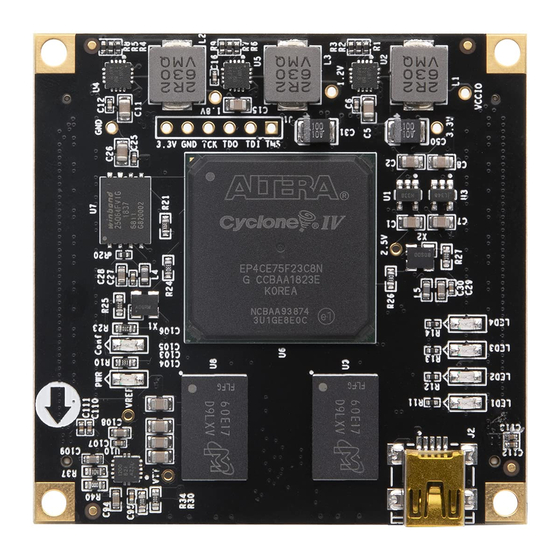
Page 4: Part 1: Ac4075 Core Board
ALINX ALTERA Core Board AC4075 User Manual Part 1: AC4075 core board Amazon Store: https://www.amazon.com/alinx 4 / 19... -
Page 5: Part 2: Ddr2 Dram
ALINX ALTERA Core Board AC4075 User Manual FPGA+ 2DDR2 core board is based on ALTERA CYCLONE IV series EP4CE75F23C8. This chip develops a high-performance core board with high speed, high bandwidth and high capacity. It is suitable for video image processing and high-speed data acquisition. - Page 6 ALINX ALTERA Core Board AC4075 User Manual address lines and control lines, and VTT voltage VREF are 0.9V. Figure 2-2 detailed the power supply schematic below: Figure 2-2: DDR2 Power for VTT/VREF Figure 2-3: DDR2 Power Circuit on the Core Board DDR2 connected to the BANK3 and BANK4 of the FPGA.
-
Page 7: Part 3: Spi Flash
ALINX ALTERA Core Board AC4075 User Manual DDR2_A[4] DDR2_BA[2] AB10 DDR2_A[5] DDR2_nCAS DDR2_A[6] DDR2_CKE DDR2_A[7] AA19 DDR2_CLK_P DDR2_A[8] DDR2_CLK_N DDR2_A[9] DDR2_DQ[16] AB18 DDR2_A[10] DDR2_DQ[17] DDR2_nRAS DDR2_DQ[18] DDR2_nWE DDR2_DQ[19] AB16 DDR2_ODT AA17 DDR2_DQ[20] DDR2_DM[0] DDR2_DQ[21] AB20 DDR2_DM[1] DDR2_DQ[22] DDR2_DM[2] AA16 DDR2_DQ[23]... - Page 8 ALINX ALTERA Core Board AC4075 User Manual and the model is M25P64, which uses the 3.3V CMOS voltage standard. Due to the non-volatile nature of SPI FLASH, it can be used as a boot device for the system to store the boot image of the system. These images mainly include FPGA bit files, core application code and other user data files.
-
Page 9: Part 4: Fpga Power Supply
ALINX ALTERA Core Board AC4075 User Manual nCSO DATA0 ASDO Part 4: FPGA Power Supply In order for FGPA to work properly, we need to provide 3.3V, 1.8V, 2.5V, 1.2V and VCCIO five-way power for the FPGA. Let's talk about the power pin portion of the FPGA, which includes the power pins for each bank, the core voltage pins, the analog voltage, and the phase-locked loop power supply pins. - Page 10 ALINX ALTERA Core Board AC4075 User Manual capacitors are used to ensure the system's power supply is stable and reliable. The three-way DCDC power supply circuit is designed as follows: Figure 4-1: DC-DC Power Supply Schematic The other two channels (3.3V and 2.5V) use less LDO chips SPX3819M5-L-3-3 and SPX3819M5-L-2-5 because of the low current required.
-
Page 11: Part 5: Expansion Ports
ALINX ALTERA Core Board AC4075 User Manual Figure 4-2: LDO Power Supply Schematic Figure 4-3: Power Supply Circuit on the Core Board Part 5: Expansion Ports The core board has a total of two high-speed expansion ports, which is connected with the FPGA carrier board by two 100-pin inter-board connectors. - Page 12 ALINX ALTERA Core Board AC4075 User Manual Figure 5-1: Expansion Ports P1 Amazon Store: https://www.amazon.com/alinx 12 / 19...
- Page 13 ALINX ALTERA Core Board AC4075 User Manual Figure 5-2: Expansion Ports P2 Amazon Store: https://www.amazon.com/alinx 13 / 19...
-
Page 14: Part 6: Power Interface On Core Board
ALINX ALTERA Core Board AC4075 User Manual Figure 5-3: Expansion Ports P1&P2 on the Core Board Part 6: Power interface on Core Board In order to make the core board work normally, the FPGA expansion board needs to provide a +5V power supply to the core board through the expansion ports. -
Page 15: Part 7: Crystal Oscillator On Core Board
ALINX ALTERA Core Board AC4075 User Manual If you need to debug the core board separately, power the core board through the Mini USB port (J2) of the core board, the Mini USB cable is connected to the USB port of the computer. -
Page 16: Part 8: Led Light On Core Board
ALINX ALTERA Core Board AC4075 User Manual Figure 7-2: Crystal oscillator on the Core Board Crystal oscillator Pin Assignment Input Clock FPGA Pin 50MHz 27MHz Part 8: LED Light on Core Board There are 6 red LED lights on the AC4075 FPGA core board, one of which is the power indicator light (PWR), one is the configuration LED light (DONE), and four are the user LED light. - Page 17 ALINX ALTERA Core Board AC4075 User Manual Figure 8-1: Power Indicator and Configure Indicator schematic Figure 8-2: Power Indicator and Configure Indicator on the Core Board The schematic diagram of the four user LED sections is shown below. In Figure 8-3, When the FPGA pin output is logic 0, the LED will be lit.
- Page 18 ALINX ALTERA Core Board AC4075 User Manual Figure 1-8-4: User LED on the Core Board User LEDs Pin Assignment LED Name FPGA Pin LED0 LED1 LED2 LED3 Amazon Store: https://www.amazon.com/alinx 18 / 19...
-
Page 19: Part 9: Structure Diagram
ALINX ALTERA Core Board AC4075 User Manual Part 9: Structure Diagram Figure 1-9-1: AC4040 FPGA Core board (Top view) Figure 1-9-2: AC4040 FPGA Core board (Top view) Amazon Store: https://www.amazon.com/alinx 19 / 19...
Need help?
Do you have a question about the ALTER AC4075 and is the answer not in the manual?
Questions and answers