Table of Contents
Advertisement
Quick Links
Advertisement
Table of Contents

Related Manuals for Advantech PCI-1716


Summary of Contents for Advantech PCI-1716
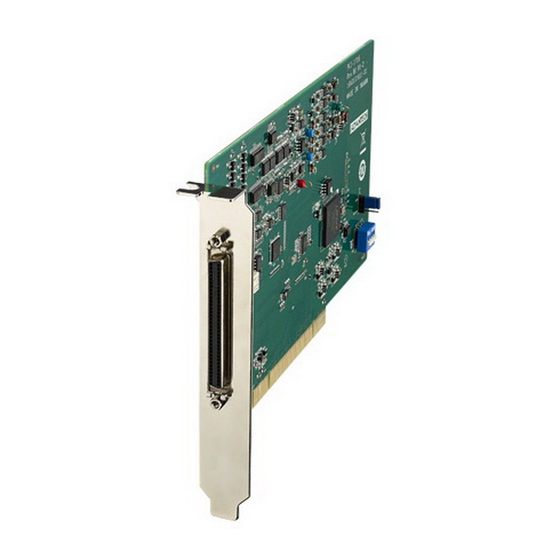
- Page 1 User Manual PCI-1716/1716H/1716L 16-bit Multi-function Card with PCI Bus...
- Page 2 Because of Advantech’s high quality-control standards and rigorous testing, most of our customers never need to use our repair service. If an Advantech product is defec- tive, it will be repaired or replaced at no charge during the warranty period. For out- of-warranty repairs, you will be billed according to the cost of replacement materials, service time and freight.
- Page 3 This product has passed the CE test for environmental specifications when shielded cables are used for external wiring. We recommend the use of shielded cables. This kind of cable is available from Advantech. Please contact your local supplier for ordering information.
- Page 4 PCI-1716_Series User Manual...
-
Page 5: Table Of Contents
Contents Chapter Introduction..........1 Features ....................2 Applications....................3 Installation Guide ..................3 Software Overview ..................3 Software Utility ..................4 Software Development Using DAQNavi SDK ........... 4 Accessories....................5 Chapter Installation Guide ........7 Unpacking ....................8 Switch and Jumper Settings..............9 Figure 2.1 Connector and Switch Locations ........ - Page 6 3.1.3 Configuration for Buffered Analog Input Acquisition ....23 Figure 3.3 Post-trigger acquisition..........24 Figure 3.4 Streaming acquisition..........24 3.1.4 External Conversion Clock with Gate ......... 24 Figure 3.5 External conversion clock with gate......24 Analog Output ..................25 3.2.1 Analog Output Resolution............
- Page 7 Figure 3.38One-shot operation........... 40 3.5.4 Timer/Pulse................. 40 Figure 3.39Pulse output and timer interrupt....... 40 Figure 3.40Gated timer/pulse output.......... 41 3.5.5 Pulse Width Modulation Output ..........41 Figure 3.41Pulse width modulation output........41 Figure 3.42Gated pulse width modulation output....... 41 Timing Signals..................
- Page 8 PCI-1716_Series User Manual viii...
-
Page 9: Chapter 1 Introduction
Chapter Introduction... -
Page 10: Features
PCI-1716/1716H/1716L offers the following main features: PCI-Bus Plug & Play The PCI-1716/1716H/1716L card uses a PCI controller to interface the card to the PCI bus. The controller fully implements the PCI bus specification Rev 2.2. All config- urations related to the bus, such as base address and interrupt assignment, are auto- matically controlled by software. -
Page 11: Applications
Process control and monitoring Vibration and transient analysis Installation Guide Before you install your PCI-1716/1716H/1716L card, please make sure you have the following necessary components: PCI-1716/1716H/1716L DA&C card PCI-1716/1716H/1716L User Manual Driver software Advantech DAQNavi software ... -
Page 12: Software Utility
All these software packages are available on the Advantech website: http://www.advantech.com/. The Advantech Navigator is a utility that allows you to set up, configure and test your device, and later store your settings in a proprietary database. -
Page 13: Accessories
Accessories Advantech offers a complete set of accessory products to support the PCI-1716/ 1716H/1716L card. These accessories include: Wiring Cables PCL-10168-1E 68-pin SCSI Shielded Cable, 1 m PCL-10168-2E 68-pin SCSI Shielded Cable, 2 m PCL-10168H-1E 68-pin SCSI Shielded Cable with Noise Rejecting, 1 m ... - Page 14 PCI-1716_Series User Manual...
-
Page 15: Chapter 2 Installation Guide
Chapter Installation Guide... -
Page 16: Unpacking
Unpacking After receiving your PCI-1716/1716H/1716L package, inspect the contents first. The package should include the following items: PCI-1716/1716H/1716L card Startup Manual The PCI-1716/1716H/1716L card harbor certain electronic components vulnerable to electrostatic discharge (ESD). ESD can easily damage the integrated circuits and certain components if preventive measures are ignored. -
Page 17: Switch And Jumper Settings
Switch and Jumper Settings Please refer to Figure 2.1 for jumper and switch locations on PCI-1716/1716H/ 1716L. Figure 2.1 Connector and Switch Locations PCI-1716_Series User Manual... -
Page 18: Board Id (Sw1)
2.2.1 Board ID (SW1) The PCI-1716/1716H/1716L has a built-in DIP switch (SW1), which is used to define each card’s board ID. When there are multiple cards on the same chassis, this board ID switch is useful for identifying each card’s device number. -
Page 19: Pin Assignments And Signal Connections
The I/O connector on the PCI-1716/1716H/1716L is a 68-pin connector that enable you to connect to accessories with the PCL-10168-1 or PCL-10168H shielded cable. Figure 2.2 shows the pin assignments for the 68-pin I/O connector on the PCI-1716/ 1716H/1716L, and Table 2.3 shows its I/O connector signal description. - Page 20 Table 2.3: I/O Connector Signal Description Signal Name Reference Direction Description AI<0..15> AGND Input Analog input terminals. Each channel pair (AI0 & AI1, AI2 & AI3, etc.) can be configured as a differential input channel or two single-ended chan- nels. AO<0..1>_REF* AGND Input...
-
Page 21: Analog Input Signal Connection
Analog Input Signal Connection An analog input channel measures the voltage (VS) of the external source. Each two channels, for example, AI0 and AI1, AI2 and AI3, etc., can be configured as a differ- ential input channel, or as two separate single-ended channels. When configured as a differential channel, even number channel is the positive terminal, and odd number channel is the negative terminal. -
Page 22: Analog Multiplexer
Each analog input channel can be configured as differential or single-ended inde- pendently by software. When an even-number channel is configured as differential, the corresponding odd-number channel will be fixed to differential automatically. 2.4.2 Analog Multiplexer The analog multiplexer routes one of the analog input channels at a time (one for sin- gle-ended configuration, and two for differential configuration) to the PGIA and ADC to be measured. - Page 23 flowing between two grounds, which generates common-mode noise for the mea- surement. This is shown in Figure 2.5. Figure 2.5 Ground loop effect. If differential (ungrounded) input configuration is used instead, the high input imped- ance of the negative input terminal prevents ground loop current from flowing, and therefore rejects the common-mode noise.
-
Page 24: Analog Output Signal Connection
In this configuration, however, the output voltage is not calibrated, and the accuracy of the output voltage depends on the accuracy of the external reference voltage. Users can perform calibration through the calibration utility in the Advantech Navigator by themselves. -
Page 25: Digital Input Signal Connection
Digital Input Signal Connection A digital input channel can perform digital input measurement. The voltage logic level between the digital input (DI) terminal and the digital ground (DGND) terminal is mea- sured. To prevent undetermined or fluctuating results when input is floating, the digi- tal input channel is internally pulled-up. -
Page 26: Digital Output Signal Connection
Digital Output Signal Connection A digital output (DO) channel can perform digital output generation. A voltage logic level is generated between the digital output (DO) terminal and the digital ground (DGND) terminal. This is shown in Figure 2.10. Figure 2.10 Digital output signal connection. Each digital output channel can source or sink only finite amount of current. -
Page 27: Counter Input Signal Connection
Counter Input Signal Connection The voltage logic level between the counter input (counter clock, counter gate, counter arm, and sample clock) terminals and the digital ground (DGND) terminal is measured. To prevent undetermined or fluctuating results when input is floating, the counter input signals are internally pulled-up. -
Page 28: Counter Output Signal Connection
Counter Output Signal Connection A voltage logic level is generated between the counter output terminal and the digital ground (DGND) terminal. This is shown in Figure 2.13. Figure 2.13 Counter output signal connection. Each counter output channel can source or sink only finite amount of current. If this limit is exceeded, the output voltage will not stay in the specified voltage logic level. -
Page 29: Chapter 3 Function Details
Chapter Function Details... -
Page 30: Analog Input
Analog Input 3.1.1 Analog Input Resolution Analog input voltage or current is measured by an ADC, which has a finite resolution. For example, a 16-bit ADC divides the input range into 65,536, which is 216, codes. These codes represent input voltage or current which are equally distributed across the input range. -
Page 31: Configuration For Buffered Analog Input Acquisition
Figure 3.2 Buffered (hardware-timed) analog input acquisition. The conversion clock can be generated internally on the device or be provided exter- nally. Refer to the device specifications for supported conversion clock sources and the maximum allowable frequency of conversion clock. The acquired samples are first accumulated in the onboard first-in-first-out (FIFO) memory of the device, and then moved to the buffer in the PC by a direct memory access (DMA) engine. -
Page 32: External Conversion Clock With Gate
Figure 3.3 Post-trigger acquisition. 3.1.3.2 Streaming Analog Input Acquisition For a streaming acquisition, the number of samples to be acquired is set to infinite. The acquisition starts when a start trigger is received and continues until a stop trig- ger is received as shown in Figure 3.4. Figure 3.4 Streaming acquisition. -
Page 33: Analog Output
Analog Output 3.2.1 Analog Output Resolution Analog output voltage or current is generated by a DAC, which has a finite resolution. For example, a 16-bit DAC divides the output range into 65,536, which is 216, codes. These codes represent output voltage or current which are equally distributed across the output range. -
Page 34: Output Status When Changing Range
Figure 3.6 Power-on glitch remover of the analog output. 3.2.3 Output Status When Changing Range When analog output range changes, the DAC setting remains unchanged, and so does the output voltage. The DAC will be updated to the new output range only when a new output value is written. - Page 35 Figure 3.8 Static (software-timed) analog output update. The advantage of state update is low latency. It is typically used for writing a single value of analog output. When updating multiple analog output channels, they can be updated asynchro- nously or synchronously. For asynchronous update, each the analog output channel is updated immediately when the value to be updated is written to the device as shown in Figure 3.9.
-
Page 36: Configuration For Buffered Analog Output Generation
3.2.4.2 Buffered (Hardware-Timed) Analog Output Generation With buffered generation, a hardware signal called sample clock controls the rate and time of generation as shown in Figure 3.11. The sample clock can be generated internally on the device or be provided externally. Refer to the device specifications for supported sample clock sources and the maximum allowable frequency of sample clock. - Page 37 Figure 3.12 One-buffered generation. The start trigger can be a software command or a hardware signal. If a hardware sig- nal is used as the start trigger, the start of generation can be delayed for a specified number of sample clock cycles after a start trigger is received. Figure 3.13 shows an example of a 2-sample delay post-trigger generation.
-
Page 38: Digital Input
Digital Input 3.3.1 Digital Input Acquisition Methods The device supports both instant (software-timed) and buffered (hardware-timed) dig- ital input acquisitions. 3.3.1.1 Instant (Software-Timed) Digital Input Acquisition With instant acquisition, the software controls the rate and time of acquisition, which is thus also called software-timed acquisition. Whenever the software sends a read command, the current status of digital input ports is returned as shown in Figure 3.15. -
Page 39: Configuration For Buffered Digital Input Acquisition
The advantages of buffered acquisition over instant acquisition include: The sample rate can be much higher. The time of sample is deterministic. Hardware triggers can be used. 3.3.2 Configuration for Buffered Digital Input Acquisition According to software configurations, buffered digital input acquisition can be classi- fied into two types: One-buffered digital input acquisition ... -
Page 40: Digital Input Interrupt
Both the start trigger and the stop trigger can come from a software command or a hardware signal. If a hardware signal is used, the start (for the start trigger) or the stop (for the stop trigger) of the acquisition can also be delayed. Refer to the device specifications for possible signal sources. -
Page 41: Digital Input Debounce Filter
3.3.5 Digital Input Debounce Filter To prevent false results such as redundant interrupts (as shown in Figure 3.23) due to noise or bouncing in the digital input signal, the digital input debounce filter can be enabled. When enabled, transient pulses with duration shorter than the filter duration will be considered as glitches and will not present in the filtered digital input signal. -
Page 42: Digital Input Status Latch
Figure 3.25 Debounce filter sample clock. Digital input debounce filter can be enabled or disabled independently for each chan- nel, and filter duration can be configured by ports (each port consists of 8 channels). Refer to the device specifications for the allowable filter duration. 3.3.6 Digital Input Status Latch When a software interrupt (or event) is generated due to digital input status changed... -
Page 43: Digital Output
Digital Output 3.4.1 Digital Output Data Generation Methods The device supports both static (software-timed) digital output update and buffered (hardware-timed) digital output generation. 3.4.1.1 Static (Software-Timed) Digital Output Update With static update, the software controls the rate and time of date, which is thus also called software-timed update. -
Page 44: Configuration For Buffered Digital Output Generation
much higher transfer rates. Buffered generation is also called hardware-timed gener- ation. The advantages of buffered generation over static update include: The generation (update) rate can be much higher. The time of sample is deterministic. Hardware triggers can be used. ... - Page 45 3.4.2.2 Streaming Digital Output Generation For a streaming generation, the number of samples to be generated is set to infinite. The generation starts when a start trigger is received and continues until a stop trig- ger is received as shown in Figure 3.31. Figure 3.31 Streaming generation.
-
Page 46: Counter
Counter 3.5.1 Event Counting In event counting mode, the counter counts the number of edges the counter clock signal generates. It can be configured as rising edge active or falling edge active, as shown in Figure 3.32 and Figure 3.33, respectively. Figure 3.32 Rising edge event counting. -
Page 47: Frequency Measurement
Figure 3.35 Instant (software-timed) event counting. The advantage of instant event counting is low latency. It is typically used for reading a single sample of counter value. 3.5.2 Frequency Measurement In frequency measurement mode, the frequency of the counter clock signal is mea- sured by one of the two measuring methods: Period inversion or counting number of pulses in fixed duration. -
Page 48: One-Shot (Delayed Pulse Generation)
Figure 3.37 Frequency measurement by counting number of pulses in fixed duration. For counter clock signal frequency higher than that specified in the previous section, this method gives a more accurate result. 3.5.3 One-Shot (Delayed Pulse Generation) In one-shot mode, when an active edge of gate signal is detected, a pulse will be generated after the specified number source clock counts. -
Page 49: Pulse Width Modulation Output
The output can be gated. If counter gate is in active level, pulses are output normally. On the other hand, if counter gate is in inactive level, output is disabled. Figure 3.40 shows an example of active high gate. Figure 3.40 Gated timer/pulse output. 3.5.5 Pulse Width Modulation Output In pulse width modulation output mode, a pulse waveform with specified high period... -
Page 50: Timing Signals
Timing Signals 3.6.1 Clock Signal The clock signal can be generated internally or provided from external source. For internal clock, when configuration is done, the clock frequency cannot be changed on the fly during the acquisition or generation operation. For external clock, on the other hand, clock frequency can be controlled by the external source in real time. -
Page 51: Calibration
Calibration The Navigator of Advantech DAQNavi provides the calibration utility to calibrate the analog input and analog output circuitry of the device. Figure 3.45 shows the inter- face of the calibration utility. Follow the instructions shown to calibration the device. -
Page 52: Firmware/Fpga Code Update
Firmware/FPGA Code Update The Navigator of Advantech DAQNavi provides the firmware/FPGA code download utility. User can use this utility to update the firmware/FPGA code of the device. Figure 3.46 shows the interface of the firmware/FPGA code download utility. To update the firmware/FPGA code, first click “Browser” button to choose the new firm- ware/FPGA code file. -
Page 53: Appendix A Specifications
Appendix Specifications... -
Page 54: Function Block
Function Block PCI-1716_Series User Manual... -
Page 55: Analog Input
Analog Input Channels 16 single-ended, 8 differential, or combination Resolution 16 bits 1 MS/s max. for PCI-1716H Convert clock rate 500 kS/s max. for PCI-1716/L Shared by all enabled channels Convert clock Internal or external source 8,192 samples Data buffer size Shared by all enabled channels ±10 V, ±5 V, ±2.5 V, ±1.25 V, ±0.625 V, 0 ~ 10 V, 0 ~ 5 V, 0 ~ 2.5 V, 0... -
Page 56: Analog Output
Analog Output (Not Available for PCI-1716L) Channels 2 single-ended Resolution 16 bits Update rate 1 MS/s max. per channel Update clock source Internal or external 8,192 samples Data buffer size Shared by all enabled channels Output range ±10 V, ±5 V, 0 ~ 10 V, 0 ~ 5 V (internal reference) Output range ±V... -
Page 57: Digital Input
Digital Input Channels 16 (2 ports) Sample rate 1 MS/s max. Sample clock source Internal or external Data buffer size 4,096 samples Input type 5 V TTL Logic high 2.0 V min. Input logic level Logic low 0.8 V max. Working voltage -0.25 V ~ 5.25 V Input protection voltage... -
Page 58: Counter
Counter Channels Resolution 32 bits Input type 5 V TTL Logic high 2.0 V min. Input logic level Logic low 0.8 V max. Working voltage -0.25 V ~ 5.25 V Input protection -0.5 V ~ 6.5 V voltage Pull-up resistor 10 kΩ... -
Page 59: External Clock Gate Input
External Clock Gate Input Input type 5 V TTL Logic high 2.0 V min. Input logic level Logic low 0.8 V max. Working voltage -0.25 V ~ 5.25 V Polarity Low level pause Input protection voltage -0.5 V ~ 6.5 V Pull-up resistor 10 kΩ... - Page 60 No part of this publication may be reproduced in any form or by any means, electronic, photocopying, recording or otherwise, without prior written permis- sion of the publisher. All brand and product names are trademarks or registered trademarks of their respective companies. © Advantech Co., Ltd. 2022...
Need help?
Do you have a question about the PCI-1716 and is the answer not in the manual?
Questions and answers