Table of Contents
Advertisement
Quick Links
Advertisement
Table of Contents

Related Manuals for Advantech PCIE-1816


Summary of Contents for Advantech PCIE-1816
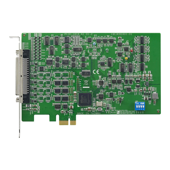
- Page 1 User Manual PCIE-1816/1816H 16-bit Multi-function Card with PCI Express Bus...
- Page 2 Because of Advantech’s high quality-control standards and rigorous testing, most of our customers never need to use our repair service. If an Advantech product is defec- tive, it will be repaired or replaced at no charge during the warranty period. For out- of-warranty repairs, you will be billed according to the cost of replacement materials, service time and freight.
- Page 3 This product has passed the CE test for environmental specifications when shielded cables are used for external wiring. We recommend the use of shielded cables. This kind of cable is available from Advantech. Please contact your local supplier for ordering information.
- Page 4 PCIE-1816_1816H User Manual...
-
Page 5: Table Of Contents
Chapter Installation..........7 Unpacking ....................8 Driver Installation ..................9 Figure 2.1 Setup Screen of Advantech Automation Software ..9 Figure 2.2 Different Options for Driver Setup ......10 Hardware Installation ................10 Device Setup & Configuration ..............11 Figure 2.3 The Device Setting of PCIE-1816/1816H ....11 Figure 2.4 The Device Setting page .......... - Page 6 B.1.6 AI Trigger Source................ 47 Table B.2: Analog Input Data Format ........47 Table B.3: Full Scale Values for Input Voltage Ranges..... 48 PCIE-1816/1816H Analog Output Operation .......... 48 B.2.1 Analog Output Ranges ............... 48 B.2.2 Analog Output Operation Modes ..........49 B.2.3...
-
Page 7: Chapter 1 Introduction
Chapter Introduction This chapter introduces PCIE- 1816/1816H and and its typical applications. Sections include: Features Applications Installation Guide Software Overview Roadmap Accessories... -
Page 8: Features
SRAM stores different gain values for each channel. This combination lets user perform multi-channel high-speed sampling for each channel. Onboard Ring Buffer Memory There are 4k sample ring buffers for AI and AO on PCIE-1816/1816H. This is an important feature for faster data transfer and more predictable performance under Windows. -
Page 9: Applications
BoardID Switch The PCIE-1816/1816H has a built-in DIP switch that helps define each card’s ID when multiple PCIE-1816/1816H cards have been installed on the same PC chassis. The BoardID setting function is very useful when building a system with multiple PCIE-1816/1816H cards. - Page 10 Figure 1.1 Installation Flow Chart PCIE-1816_1816H User Manual...
-
Page 11: Software Overview
Software Overview Advantech offers a rich set of DLL drivers, third-party driver support and application software to help fully exploit the functions of your PCIE-1816/1816H card: Device Drivers (on the companion DVD-ROM) LabVIEW driver Advantech DAQ NAVi ... -
Page 12: Accessories
Advantech Navigator. Programming with DAQNavi Device Drivers Function Library Advantech DAQNavi Device Drivers offer a rich function library that can be utilized in various application programs. This function library consists of numerous APIs that support many development tools, such as Visual Studio .Net, Visual C++, Visual Basic, Delphi and C++ Builder. -
Page 13: Chapter 2 Installation
Chapter Installation This chapter provides a packaged item checklist, proper instructions for unpacking and step-by-step procedures for both driver and card installation. Sections include: Unpacking Driver Installation Hardware Installation Device Setup & Configuration... -
Page 14: Unpacking
Unpacking After receiving your PCIE-1816/1816H package, inspect the contents first. The pack- age should include the following items: PCIE-1816/1816H card Companion DVD-ROM (Device Drivers included) Startup Manual The PCIE-1816/1816H card harbor certain electronic components vulnerable to elec- trostatic discharge (ESD). -
Page 15: Driver Installation
Driver Installation We recommend you to install the driver before you install the PCIE-1816/1816H card into your system, since this will guarantee a smooth installation process. The Advantech DAQNavi Device Drivers Setup program for the PCIE-1816/1816H card is included in the companion DVD-ROM that is shipped with your DA&C card package. -
Page 16: Hardware Installation
Make sure you have installed the driver first before you install the card (refer to 2.2 Driver Installation) After the Device Drivers installation is completed you can install the PCIE-1816/ 1816H card on your computer. However, it is suggested that you refer to the com- puter’s user manual or related documentation if you have any doubts. -
Page 17: Device Setup & Configuration
Setup, Configuration and Testing of your device. Device Setup & Configuration The Advantech Navigator program is a utility that allows you to set up, configure and test your device, and later stores your settings on the system registry. These settings will be used when you call the APIs of Advantech Device Drivers. - Page 18 Configuring the Device Please go to the Device Setting to configure your device. Here you can config- ure not only the Analog Input/Output of PCIE-1816/1816H but also Digital Input/ Output. Figure 2.4 The Device Setting page After your card is properly installed and configured, you can go to the Device Test page to test your hardware by using the testing utility supplied.
-
Page 19: Chapter 3 Signal Connections
Chapter Signal Connections This chapter provides useful information about how to connect input and output signals to the PCIE-1816/1816H card via the I/O connector. Sections include: Overview BoardID Settings Signal Connections Field Wiring Considerations... -
Page 20: Overview
This chapter provides useful information about how to connect input and output signals to the PCIE-1816/1816H card via the I/O connector. Switch and Jumper Settings Please refer to Figure 3.1 for jumper and switch locations on PCIE-1816/1816H. Figure 3.1 Connector and Switch Locations PCIE-1816_1816H User Manual... -
Page 21: Board Id (Sw1)
3.2.1 Board ID (SW1) The PCIE-1816/1816H has a built-in DIP switch (SW1), which is used to define each card’s board ID. When there are multiple cards on the same chassis, this board ID switch is useful for identifying each card’s device number. -
Page 22: Jumper Settings To Set Ports As Software-Configurable Or Output Ports
3.2.3 Jumper Settings to Set Ports as Software-configurable or Output ports Table 3.3: Function Description Set DIO channel as software-configurable input or output (default) Set DIO channel as output Jumper number Relative channels JP1600 DIO 0~3 JP1601 DIO 4~7 JP1700 DIO 8~11 JP1701 DIO 12~15... -
Page 23: Signal Connections
Signal Connections Pin Assignments The I/O connector on the PCIE-1816/1816H is a 68-pin connector that enable you to connect to accessories with the PCL-10168-1 or PCL-10168H shielded cable. Figure 3.2 shows the pin assignments for the 68-pin I/O connector on the PCIE-1816/ 1816H, and Table 3.3 shows its I/O connector signal description. -
Page 24: I/O Connector Signal Description
AGND Analog Ground. These pins are the reference points for single-ended measurements and the bias current return point for differential measure- ment. The ground reference (AGND and DGND) are connected together on the PCIE-1816/ 1816H. ATRG0 AGND Input Analog Threshold Trigger. These pins are the ATRG1 analog input threshold trigger input. -
Page 25: Analog Input Connections
(0.3A maximum) 3.3.2 Analog Input Connections PCIE-1816/1816H supports either 16 single-ended or 8 differential analog inputs. Single-ended Channel Connections The single-ended input configuration has only one signal wire for each channel, and the measured voltage (Vm) is the voltage of the wire as referenced against the com- mon ground. - Page 26 PCIE-1816/1816H. With this connection, the PGIA rejects a common-mode voltage Vcm between the signal source and the PCIE-1816/1816H ground, shown as Vcm in Figure 3-4. Figure 3.4 Differential input channel connections...
- Page 27 If a floating signal source is connected to the differential input channel, the signal source might exceed the common-mode signal range of the PGIA, and the PGIA will be saturated with erroneous voltage-readings. You must therefore reference the sig- nal source against the AGND. Figure 3-5 shows a differential channel connection between a floating signal source and an input channel on the PCI-1816/1816H.
- Page 28 However, this connection has the disadvantage of loading the source down with the series combination (sum) of the two resistors. For ra and rb, for example, if the input impedance rs is 1k Ohm, and each of the two resistors is 100k Ohm, then the resis- tors load down the signal source with 200 Ohm (100 Ohm+ 100 Ohm), resulting in a - 0.5% gain error.
- Page 29 External AI Sample Clock The external AI sample clock is useful when you want to pace acquisitions at rates not available with the internal AI sample clock, or when you want to pace at uneven intervals. Connect an external AI sample clock to screw terminal AI_CLK on the screw terminal board.
- Page 30 (rising edge). User should connect analog signals from external device or analog out- put channel on board to external input signal ATRG0 and ATRG1. On the PCIE-1816/ 1816H, the threshold level is set using a dedicated 16-bit DAC. By software, you can program the threshold level by writing a voltage value to this DAC;...
- Page 31 Fig. 3.9 shows how to make analog output and external reference input connections on the PCIE-1816/1816H. Figure 3.9 Analog Output Connections PCIE-1816_1816H User Manual...
- Page 32 An external digital trigger event occurs when the PCIE-1816/ 1816H detects either a rising or falling edge on the External AO TTL trig- ger input signal from the pin of connector. User can define the type of trigger source as rising-edge or falling-edge by software.
-
Page 33: Digital Signal Connections
Analog Threshold Trigger For analog input operations, an analog trigger event occurs when the PCIE-1816/ 1816H detects a transition from above a threshold level to below a threshold level (falling edge), or a transition from below a threshold level to above a threshold level (rising edge). - Page 34 Figure 3.14 Wet signal connection of digital input Figure 3.15 Dry signal connection of digital input Digital Output Connections PCIE-1816/ 1816H also has TTL digital output Figure 3.16 Digital Output Channel Connections PCIE-1816_1816H User Manual...
-
Page 35: Field Wiring Considerations
Field Wiring Considerations When you use PCIE-1816/1816H cards to acquire data from outside, noise in the environment might significantly affect the accuracy of your measurements if due cau- tions are not taken. The following measures will be helpful to reduce possible interfer- ence running signal wires between signal sources and the PCIE-1816/1816H card. - Page 36 PCIE-1816_1816H User Manual...
-
Page 37: Appendix A Specifications
Appendix Specifications... -
Page 38: Function Block
Function Block PCIE-1816_1816H User Manual... -
Page 39: Analog Input
Analog Input Channels 16 single-ended / 8 differential Resolution 16-bit Built-in memory 4K samples Model PCIE-1816 PCIE-1816H Single-channel 1 MS/s 5 MS/s Sampling Rate Multi-channel 500 KS/s 1 MS/s Unipolar/Bipolar 100 KS/s 250 KS/s Mixed Gain Input Range and Gain List... -
Page 40: Analog Output
Analog Output Channels Resolution 16-bit Memory Size 4k samples Update Rate 3 MS/s Internal Reference 0~5, 0~10, ±5, ±10 V External Reference Reference Input Maximum Range Output Range Unipolar 0 ~ x V ≤ ≤ Bipolar -x V ~ x V -10V Accuracy Relative... -
Page 41: Counter/Timer
Counter/Timer Channels 2 channels (independent) Resolution 32-bit Compatibility TTL level Clock Source Internal 20MHz or external clock (10 MHz max.). Selected by software Output Frequency Max. 10MHz 0.8 V max. Clock Input High 2.0 V min. 0.8 V max. Gate Input High 2.0 V min. - Page 42 PCIE-1816_1816H User Manual...
-
Page 43: Appendix B Operation Theory
Appendix Operation Theory... -
Page 44: Analog Input Operation
Analog Input Operation This section describes the following features of analog input that can help you realize how to configure the functions and parameters to match various applications. AI Hardware Structure Analog input ranges and gains Analog data acquisition mechanism ... -
Page 45: Analog Input Ranges And Gains
±10 V FSR. The PCIE-1816/1816H provides various program- mable gain levels and each channel is allowed to set its own input range individually. Table B.1 lists the effective ranges supported by the PCIE-1816/1816H with gains. Table B.1: Gains and Analog Input Range... - Page 46 Double-Clock Procedure Double clock procedure is the fundamental AI conversion mechanism of the PCIE- 1816/1816H, regardless of which mode selected. The incoming SCAN CLK launches an acquisition period called Acquisition Window. The arriving CONV CLKs within the Acquisition Window will become an efficient AI conversion clock to trigger AI con- verter.
- Page 47 Other scanning procedure applications timing diagram. PCIE-1816_1816H User Manual...
- Page 48 Single Clock Source Driving Single clock source driving is a specific function well-suited for consecutive data acquisition while there is only one clock signal available. CONV CLKs will be inter- nally routed as SCAN CLKs. And the external SCAN CLKs input will not be accepted. Figure describes how it works.
-
Page 49: Ai Trigger Modes
B.1.4 AI Trigger Modes The PCIE-1816/1816H supports four trigger modes and pause function. User can start or stop the operation by trigger mode selection. An extra 32-bit counter is dedi- cated to delay-trigger mode and about-trigger mode, and user can set it as the num- ber of delay SCAN CLKs before trigger or the number of holding SCAN CLKs after trigger. - Page 50 SCAN CLKs has been taken after the trigger event. User can set the delay number of SCAN CLKs by a 32-bit counter. Delay to start trigger acquisition starts when the PCIE-1816/1816H detects the trig-ger event and stops when you stop the operation.
- Page 51 Stop Trigger Acquisition Mode Stop trigger mode is a particular application of about-trigger mode. Use pre-trigger acquisition mode when you want to acquire data before a specific trigger event occurs. Stop-trigger acquisition starts when you start the operation and stops when the trigger event happens.
-
Page 52: Ai Scan/Conv Clock Source
B.1.5 AI SCAN/CONV Clock Source The PCIE-1816/1816H can adopt both internal and external clock sources to accom- plish pacer acquisition. You can set the clock and trigger sources conveniently by software. The figure can help you understand the routing route of clock and trigger generation. -
Page 53: Ai Trigger Source
External digital (TTL) trigger Analog threshold trigger With PCIE-1816/1816H, user can also define the type of trigger source as rising- edge or falling-edge. These following sections describe these trigger sources in more detail. External Digital (TTL) Trigger... -
Page 54: Pcie-1816/1816H Analog Output Operation
0 ~ 1.25 V 1.25 ± 0.625 V 1.25 PCIE-1816/1816H Analog Output Operation The PCIE-1816/1816H card provides two 16-bit multi-range analog output (D/ A) channels. This section describes the following features: Analog output ranges Analog output operation modes ... -
Page 55: Analog Output Operation Modes
PC. The host computer then transfers that data to the DACs’ buffers on PCIE-1816/1816H. When PCIE-1816/1816H detects a trigger, it outputs the values stored in its buffer. When the buffer’s storage decreases, the card sends an interrupt request to the host PC which in turn sends samples to the buffer. -
Page 56: Ao Clock Sources
B.2.3 AO Clock Sources The PCIE-1816/1816H can adopt both internal and external clock sources for pacing the analog output of each channel: Internal AO output clock with 32-bit Divider External AO output clock from connector The internal and external AO output clocks are described in more detail as follows: ... -
Page 57: Digital Input/Output Operation
Digital Input/Output Operation The PCIE-1816/1816H supports 24 digital I/O channels. You can use each byte as either an input port or an output port by configuring the corresponding parameter; and all four channels of the byte have the same configuration. - Page 58 Frequency Measurement Connection PCIE-1816/ 1816H built-in counter can measure the frequency value of the sig- nal connected to counter input. Pulse Width measurement Connection PCIE-1816/1816H built-in counter can measure the pulse width value of the sig- nal connected to counter input. The measurable range is 50 ns to 107 seconds.
- Page 59 0.005 Hz ~ 5 MHz. Delay Pulse Generation Using PCIE-1816/1816H internal clock, you can change the logic level within a specific period, starting from a trigger signal connecting to counter gate input. For example, if you define the count equals to 3 (as figure below), a counter out- put will change its status after 3 pulses of internal clock signals pass, after a trig- ger signal from counter gate becomes high.
- Page 60 PWM Output: PCIE-1816/1816H can generate PWM (pulse width modulation) signal which you can configure its logic high time and logic low time as figure below. The available period range for logic high time and logic low time is 100 ns ~ 214 second.
- Page 61 PCIE-1816_1816H User Manual...
- Page 62 No part of this publication may be reproduced in any form or by any means, electronic, photocopying, recording or otherwise, without prior written permis- sion of the publisher. All brand and product names are trademarks or registered trademarks of their respective companies. © Advantech Co., Ltd. 2019...
Need help?
Do you have a question about the PCIE-1816 and is the answer not in the manual?
Questions and answers