
Related Manuals for Advantech PCI-1720


Summary of Contents for Advantech PCI-1720
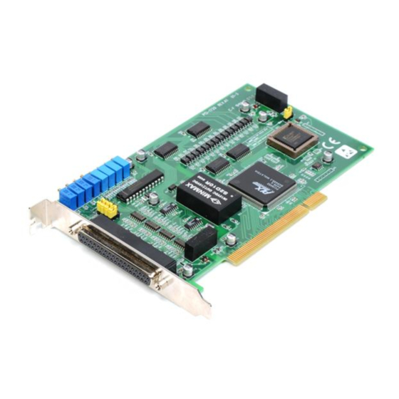
- Page 1 PCI-1720 4-ch Isolated Analog Output Card PCI-1720U 4-ch Isolated Analog Output Card with Universal PCI Bus User Manual...
- Page 2 Acknowledgments PC-LabCard is a trademark of Advantech Co., Ltd. IBM and PC are trademarks of International Business Machines Corporation. MS-DOS and Windows are trademarks of Microsoft Corporation. Intel and Pentium are trademarks of Intel Corporation.
- Page 3 Product Warranty (2 years) Advantech warrants to you, the original purchaser, that each of its prod- ucts will be free from defects in materials and workmanship for two years from the date of purchase. This warranty does not apply to any products which have been repaired or...
- Page 4 CE Notification PCI-1720 and PCI-1720U have passed the CE test for environmental specifications when shielded cables are used for external wiring. We rec- ommend the use of shielded cables. This kind of cable is available from Advantech. Please contact your local supplier for ordering information.
-
Page 5: Table Of Contents
2 Installation ............6 2.1 Unpacking..................6 2.2 Driver Installation................ 7 Figure 2.1: Setup Screen of Advantech Automation Software 7 Figure 2.2: Different Options for Driver Setup ......8 2.3 Hardware Installation ..............9 Figure 2.3: The Device Name Listed on Device Manager ..10 2.4 Device Setup and Configuration .......... - Page 6 Appendix A Calibration ............. 36 A.1 Overview ................... 36 A.2 Starting Calibration..............37 Figure A.1: PCI-1720U VR assignment ......... 37 A.3 Unipolar Output Calibration............38 A.4 Bipolar Output Calibration ............38 A.5 Current Sink Calibration............38 PCI-1720 & 1720U User Manual...
- Page 7 General Information...
-
Page 8: Chapter 1 General Information
PCI-bus Plug & Play The PCI-1720 cards use a PCI controller to interface the cards to the PCI bus. The controller fully implements the PCI bus specification Rev 2.1. All bus relative configurations, such as base address and interrupt assign- ment, are automatically controlled by software. -
Page 9: Applications
1.3 Applications • Process control • Programmable voltage source • Programmable current sink • Servo control 1.4 Specifications D/A Output • Channels: 4 isolated D/A channels • Resolution: 12 bits • Output Ranges:Unipolar: 0 ~ +5 V, 0 ~ +10 V Bipolar: ±5 V, ±10 V Current loop (sink): 0 ~ 20 mA, 4 ~ 20 mA •... -
Page 10: Block Diagram
(refer to IEC 68-2-3) • MTBF: over 71,280 hrs @ 25° C, grounded, fixed environment 1.5 Block Diagram Control Controller Logic Decoder Data Buffer Data Buffer Isolation 2500 V 4 Ch 12 Bit D/A Range Control PCI-1720 & 1720U User Manual... - Page 11 Installation This chapter gives users a package item checklist, proper instructions for unpacking and step-by-step procedures for both driver and card installation. Sections include: • Unpacking • Driver Installation • Hardware Installation • Device Setup and Configuration...
-
Page 12: Chapter 2 Installation
Chapter 2 Installation 2.1 Unpacking After receiving your PCI-1720 package, please inspect its contents first. The package should contain the following items: • PCI-1720 or PCI-1720U card • Companion CD-ROM (Device Drivers included) • User Manual PCI-1720 cards harbors certain electronic components vulnerable to elec- trostatic discharge (ESD). -
Page 13: Driver Installation
PC or transport it elsewhere. 2.2 Driver Installation We recommend you to install the driver before you install the PCI-1720 card into your system, since this will guarantee a smooth installation pro- cess. -
Page 14: Figure 2.2: Different Options For Driver Setup
Figure 2.2: Different Options for Driver Setup For further information on driver-related issues, an online version of the Device Drivers Manual is available by accessing the following path: Start/Programs/Advantech Automation/Device Manager/Device Driver's Manual PCI-1720 & 1720U User Manual... -
Page 15: Hardware Installation
2.3 Hardware Installation Make sure you have installed the driver first before you install the card (please refer to 2.2 Driver Installation). After the Device Drivers installation is completed, you can then install the PCI-1724U card into any PCI slot on your computer. However, it is suggested that you refer to the computer user’s manual or related docu- mentation if you have any doubt. - Page 16 Then go through the driver installation process again. After your card is properly installed on your system, you can now config- ure your device using the Advantech Device Manager Program that has itself already been installed on your system during driver setup. A com- plete device installation procedure should include device setup, configu- ration and testing.
-
Page 17: Device Setup And Configuration
2.4 Device Setup and Configuration The Advantech Device Manager program is a utility that allows you to set up, configure and test your device, and later stores your settings on the system registry. These settings will be used when you call the APIs of Advantech Device Drivers. -
Page 18: Configuring The Device
Appendix D Calibration Util- ity. Figure 2.5: The Device Setting dialog box Note: Users have three options for the output voltage ranges and current ranges: -10 ~ 10 V, 0 ~ 20 mA and 4 ~ 20 mA. PCI-1720 & 1720U User Manual... - Page 19 After you have finished configuring the device, click OK and the device name will appear in the Installed Devices box as seen below: Figure 2.6: Device Name Appearing on the List of Devices Box After your card is properly installed and configured, you can click the Test…...
- Page 20 PCI-1720 & 1720U User Manual...
- Page 21 Jumpers and I/O Connectors...
-
Page 22: Chapter 3 Jumpers And I/O Connectors
Chapter 3 Jumpers and I/O Connectors PCI-1720 cards are Plug & Play compatible, i.e. the system BIOS assigns the system resources such as the base address and the interrupt number automatically. There are only 2 functions with 5 jumpers to configure to your applications requirements. -
Page 23: Jumper Jp5 Setting For The Reset State
Note! In order to maintain accurate outputs for your field applications, it is important that you calibrate the PCI-1720U’s variable resistors (VRs) from time to time. Calibration instructions are pro- vided in Appendix A. 3.1.2 Jumper JP5 Setting for the Reset State Jumper JP5 gives the PCI-1720U a new and valuable capability. -
Page 24: Connector And Pin Assignments
3.2 Connector and Pin Assignments PCI-1720 cards use one DB-37 female connector, which is located on the card at CN1 (see Figure 3-1) and connects D/A signals to external devices. The following figure shows the pin assignments of the connec- tor. -
Page 25: Signal Descriptions Of I/O Connector
3.2.1 Signal Descriptions of I/O Connector Signal Name Reference Direction Description VOUT<0...3> AGND Output Analog Voltage Output Channels 0 through 3. These pins supply the voltage outputs for the analog outputs. ISINK<0...3> AGND Input Current Sink Channels 0 through 3. These pins provide the current loop sink input. -
Page 26: Setting The Boardid Switch (Sw1)
This unique identifier has been set to 0 with the BoardID switch at the factory. If you need to adjust it to other numbers, set SW1 by referring to DIP switch setting. Table 3.1: Board ID Setting (SW1) BoardID 0 (default) PCI-1720 & 1720U User Manual... -
Page 27: Identity Register
3.3.1 Identity Register You can determine the identity in the register as shown in the table below. Table 3.2: Identity Register of PCI-1720U Base+20 Abbreviation Note: ID0: The least significant bit (LSB) of identifier ID3: The most significant bit (MSB) of identifier Chapter 3... - Page 28 PCI-1720 & 1720U User Manual...
- Page 29 Register Structure and Format...
-
Page 30: Chapter 4 Register Structure And Format
Chapter 4 Register Structure and Format 4.1 Overview PCI-1720 cards are delivered with an easy-to-use 32-bit DLL driver for user programming under Windows 98, 2000 and XP operating systems. We advise users to program the card using the 32-bit DLL driver pro- vided by Advantech to avoid the complexity of low-level programming by register. -
Page 31: I/O Port Address Map
4.2 I/O Port Address Map PCI-1720 cards require 12 addresses in the PC’s I/O space. The address of each register is specified as an offset from the card’s base address. For example, BASE + 0 is the card’s base address and BASE + 7 is the base address plus seven bytes. -
Page 32: D/A Output Channel 0 To 3
Table 4.4: Output Range of D/A Channel n D An_U/B D An_5/10 D/A channel n output range 0 to +5 V 0 to +10 V -5 to +5 V -10 to +10 V * n = 0,1,2,3. PCI-1720 & 1720U User Manual... -
Page 33: Synchronized Output Prompt Register
4.2.3 Synchronized Output Prompt Register During normal operation, the card will accept digital values one at a time from the host PC, convert these values to analog values, and immediately output these analog values from the channels directed by the host PC. -
Page 34: Unipolar And Bipolar Binary Code Tables
1. Vref is the reference source voltage that you selected. Vref is +5 V or +10 V. 2. Nominal full scale is given by FS = Vref ( (2047/2048). 3. Nominal LSB magnitude is given by LSB = Vref ( (1/2048). PCI-1720 & 1720U User Manual... - Page 35 Signal Connections...
-
Page 36: Chapter 5 Signal Connections
This chapter shows you how to make proper signal connections. 5.2 D/A Voltage Output Connections PCI-1720 cards support four channels of D/A voltage output. Only one output signal wire is used with each channel. The voltage output is refer- enced to a common ground (AGND). - Page 37 Internal Side External Side Grounded Load AGND Figure 5.2: Grounded-load Connection for D/A Voltage Output Internal Side External Side Diff. Load with Ground AGND Figure 5.3: Differential-load Connection for D/A Voltage Output Chapter 5...
-
Page 38: Current Sink Connections
5.3 Current Sink Connections The PCI-1720 cards’ current loop output uses a 0 to +5 V (unipolar) volt- age output as each channel’s driving source. Current drive circuits con- sist of a power field-effect transistor (FET). The current output’s voltage bias must be less then 50 V for accurate results. -
Page 39: Figure 5.6: Floating-Load Conn. With An Internal +12 Vdc Pow Er Supply
Figure 5.6: Floating-load Conn. with an Internal +12 VDC Power Supply 5.4 Current Sink Load and Power Supply You have to select the current sink load and power supply carefully. The current sink circuitry of the PCI-1720 cards is as shown below. Internal Side External Side... - Page 40 1.75 kW (40 / 0.02 - 249 > RL). Select RL = 200 W, PD = 0.62 > 0.2 fail! Reselect RL = 1 kW, PD = 0.3 > 0.2 fail! Reselect RL = 1.5 kW, PD = 0.1 < 0.2 OK! PCI-1720 & 1720U User Manual...
- Page 41 Calibration This appendix provides brief informa- tion on PCI-1720 cards calibration. Regular calibration checks are impor- tant to maintain accuracy in data acqui- sition and control applications.
-
Page 42: Appendix A Calibration
Appendix A Calibration A.1 Overview PCI-1720 cards are calibrated at the factory for initial use. However, a recalibration of the analog analog outputs is recommended: 1. Every six months. 2. Everytime the analog output range is changed. We provide a calibration program on the companion CD-ROM. The cali- bration programs make calibration easier. -
Page 43: Starting Calibration
A.2 Starting Calibration PCI-1720 cards use eight variable resistors (VRs), two for each channel, which allow you to calibrate each of the card’s four output channels. The following information outlines the function of each VR. Refer to the illus- tration shown below for the locations of the VRs. -
Page 44: Unipolar Output Calibration
Set all digital input codes to 1. Now, adjust VRn (n = 1, 2, 3, 4 depending on what channel is to be calibrated, see prior page) until your ammeter shows a reading equal to 20.00 mA. Repeat steps 2 and 3 until both of them are satisfied. PCI-1720 & 1720U User Manual...
Need help?
Do you have a question about the PCI-1720 and is the answer not in the manual?
Questions and answers