Table of Contents
Advertisement
Quick Links
Advertisement
Table of Contents

Subscribe to Our Youtube Channel
Related Manuals for Advantech PCIE-1810


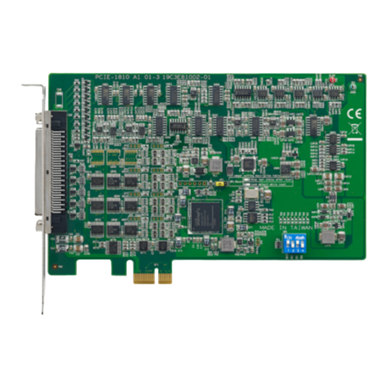
Summary of Contents for Advantech PCIE-1810
- Page 1 User Manual PCIE-1810 12-bit Multifunction Card with PCI Express Bus...
- Page 2 No part of this manual may be reproduced, copied, translated, or transmitted in any form or by any means without the prior written permission of Advantech Co., Ltd. The information provided in this manual is intended to be accurate and reliable.
- Page 3 This product has passed the CE test for environmental specifications when shielded cables are used for external wiring. We recommend the use of shielded cables. This type of cable is available from Advantech. Please contact your local supplier for ordering information.
- Page 4 Document Feedback To assist us with improving this manual, we welcome all comments and constructive criticism. Please send all feedback in writing to support@advantech.com. Safety Precaution - Static Electricity Follow these simple precautions to protect yourself from harm and the products from damage.
- Page 5 In accordance with IEC 704-1:1982 specifications, the sound pressure level at the operator’s position does not exceed 70 dB (A). DISCLAIMER: These instructions are provided according to IEC 704-1 standards. Advantech disclaims all responsibility for the accuracy of any statements contained herein. PCIE-1810 User Manual...
- Page 6 PCIE-1810 User Manual...
-
Page 7: Table Of Contents
Figure 2.14Pin assignment ............16 Table 2.4: Pin assignment ............17 Grounding Considerations ..............18 2.4.1 Signal Source Type..............18 Figure 2.15Signal source type ............ 18 2.4.2 Measuring a Grounded Signal Source........18 Figure 2.16Ground loop effect ............ 18 PCIE-1810 User Manual... - Page 8 Figure 3.24Pulse width modulation output ......... 34 Figure 3.25Finite pulse generation ..........34 Figure 3.26Infinite pulse generation ........... 35 Figure 3.27Gated pulse width modulation output ....... 35 Figure 3.28Static (software-timed) timer/pulse......35 Clock ....................... 35 Synchronization ..................36 PCIE-1810 User Manual viii...
- Page 9 Multi-Device Synchronization Interface (MDSI) ........46 Counter ....................47 FPGA Code Update ................48 A.10 General Specifications ................48 A.10.1 Power Requirements ..............48 A.10.2 Power Supply Output ..............48 A.10.3 Physical..................48 A.10.4 Environmental ................48 PCIE-1810 User Manual...
- Page 10 PCIE-1810 User Manual...
-
Page 11: Chapter 1 Start Using Pcie-1810
Chapter Start Using PCIE-1810... -
Page 12: Product Overview
(except for 0) for hardware devices with the same model name. Refer to the device specifications for the configuration of the board ID. If changed, the new board ID value takes effect only after cold resetting the device. PCIE-1810 User Manual... -
Page 13: Driver Installation
DAQ devices. All these software packages are available on Advantech website: http://www.advantech.com/. The Advantech Navigator is a utility that allows you to set up, configure and test your device, and later stores your settings in a proprietary database. -
Page 14: Software Development Using Daqnavi Sdk
FPGA Code Updates The FPGA can also be updated via the interface in Navigator. However, it is not advised to update FPGA without first doing some research. Advantech strongly sug- gests you consult your technical support before starting an FPGA update. -
Page 15: Chapter 2 Installation Guide
Chapter Installation Guide... -
Page 16: Initial Unpacking Check
Startup or User Manual Hardware Installation and Configuration 2.2.1 Installation Before you install your PCIE-1810, please make sure you have the following compo- nents: PCIE-1810 card PCIE-1810 User Manual Advantech DAQNavi SDK and the corresponding device driver ... -
Page 17: Configuration - Board Id (Sw1)
Configuration - DI/O Control Selection (JP2 ~ JP7) Table 2.2: Jumper Setting Description Software configurable.* Force output. * Default setting. Table 2.3: Jumper Number Relative channels DIO 0-3 DIO 4-7 DIO 8-11 DIO 12-15 DIO 16-19 DIO 20-23 * Default setting. PCIE-1810 User Manual... -
Page 18: Signal Connection And Pin Assignment
ADC in channel by channel order. That is, only one channel at a time is being converted. This architecture is called multiplexed analog input. Analog input signal connection and internal functional block diagram is shown in Figure 2. 1. Figure 2.1 Analog input signal connection PCIE-1810 User Manual... -
Page 19: Analog Output Signal Connection
In this configuration, however, the output voltage is not calibrated, and the accuracy of the output voltage depends on the accuracy of the external reference voltage. Users can perform calibration through the calibration utility in the Advantech Navigator by themselves. -
Page 20: Trigger Input Signal Connection
And another trigger occurs only if the signal has crossed the voltage specified by the threshold level minus the hysteresis value from above before it crosses the threshold level from below again. This is shown in Figure 2. 5. Figure 2.5 Rising edge active analog trigger PCIE-1810 User Manual... -
Page 21: Digital Input Signal Connection
Refer to the device specifications for ON and OFF state voltage ranges. The digital input channel can also sense the status of an external switch. When con- figured as internally pulled-up, the status of an external switch which is connected PCIE-1810 User Manual... - Page 22 Figure 2. 9. Be sure the voltage of the external source is within the allowable range of ON state as specified in the device specifications. Figure 2.8 Digital input signal connection using a switch with internally pulled- Figure 2.9 Digital input signal connection using a switch with internally pulled- down PCIE-1810 User Manual...
-
Page 23: Digital Output Signal Connection
Each digital output channel can source or sink only finite amounts of current. If this limit is exceeded, the output voltage will not stay in the specified voltage logic level. Refer to the device specifications for the maximum source and sink current values. PCIE-1810 User Manual... -
Page 24: Counter Input Signal Connection
OFF state. Moreover, avoid supplying a voltage exceeding the maximum allowed ON state value or going below the minimum allowed OFF state value, as it may dam- age the device. Refer to the device specifications for the specified voltage ranges in the ON and OFF states. PCIE-1810 User Manual... -
Page 25: Counter Output Signal Connection
Each counter output channel can source or sink only a finite amount of current. If this limit is exceeded, the output voltage will not stay in the specified voltage logic level. Refer to the device specifications for the maximum source and sink current values. PCIE-1810 User Manual... -
Page 26: Pin Assignment (Cn4)
2.3.8 Pin Assignment (CN4) Figure 2.14 Pin assignment PCIE-1810 User Manual... - Page 27 Counter clock input terminals. 4, 38 CNT<0..1>_OU Counter output terminals. 3, 37 CNT<0..1>_GA Counter gate input terminals. 2, 36 DGND Ground terminals for digital signals. 5, 14, 39, 48 +12V +12 V supply output. +5 V supply output. PCIE-1810 User Manual...
-
Page 28: Grounding Considerations
Figure 2. 16. Figure 2.16 Ground loop effect If differential (ungrounded) input configuration is used instead, the high input imped- ance of the negative input terminal prevents ground loop current from flowing, and therefore rejects the common-mode noise. PCIE-1810 User Manual... -
Page 29: Measuring An Ungrounded (Floating) Signal Source
However, this will lead to an unbalanced system if the source impedance is relatively high. A balanced system is desirable from a noise immunity point of view. PCIE-1810 User Manual... -
Page 30: Field Wiring Considerations
Board ID Configuration The PCIE-1810 has a built-in DIP switch (SW1), which is used to define each card’s board ID. When there are multiple cards on the same chassis, this board ID switch is useful for identifying each card’s device number. -
Page 31: Chapter 3 Functions Details
Chapter Functions Details... -
Page 32: Analog Input
Figure 3. Figure 3.1 Instant (software-timed) analog input acquisition The advantage of instant acquisition is low latency. It is typically used for reading a single sample of analog input. PCIE-1810 User Manual... -
Page 33: Buffered (Hardware-Timed) Analog Input Acquisition
Buffered acquisition is also called hardware-timed acquisition. The advantages of buffered acquisition over instant acquisition include: The sample rate can be much higher. The time of sample is deterministic. Hardware triggers can be used. PCIE-1810 User Manual... -
Page 34: Analog Output
The update then occurs simulta- neously for all analog output channels when the synchronous write command is issued. This is shown in Figure 3. 5. Figure 3.4 Analog output asynchronous update PCIE-1810 User Manual... -
Page 35: Buffered (Hardware-Timed) Analog Output Generation
Buffered generation is also called hardware-timed generation. The advantages of buffered generation over static update include: The generation (update) rate can be much higher. The time of sample is deterministic. Hardware triggers can be used. PCIE-1810 User Manual... -
Page 36: Digital Input
Figure 3. 7. Figure 3.7 Instant (software-timed) digital input acquisition The advantage of instant acquisition is low latency. It is typically used for reading a single sample of digital input. PCIE-1810 User Manual... -
Page 37: Buffered (Hardware-Timed) Digital Input Acquisition
Buffered acquisition is also called hardware-timed acquisition. The advantages of buffered acquisition over instant acquisition include: The sample rate can be much higher. The time of sample is deterministic. Hardware triggers can be used. PCIE-1810 User Manual... -
Page 38: Digital Output
(DMA) engine, and placed on the digital output channels one sample at a time. A buffer is a block of memory in the PC for temporar- ily storing the data to be transferred to the onboard FIFO. Because the data is moved PCIE-1810 User Manual... -
Page 39: Counter
Figure 3. 11 and Figure 3. 12, respectively. Figure 3.11 Rising edge event counting Figure 3.12 Falling edge event counting Counting may be temporarily paused by the counter gate signal as shown in Figure 3. 13. Figure 3.13 Event counting with pause gate PCIE-1810 User Manual... -
Page 40: Frequency Measurement
Figure 3.15 Frequency measurement by period inversion This method is suitable if the counter clock signal frequency is much smaller (< 0.1%) than the internal clock frequency. Measuring accuracy degrades as the counter clock signal frequency increases. PCIE-1810 User Manual... - Page 41 Whenever the software sends a read command, the current value of the frequency is returned as shown in Figure 3. 17. Figure 3.17 Instant (software-timed) frequency measurement The advantage of instant frequency measurement is low latency. It is typically used for reading a single sample of frequency value. PCIE-1810 User Manual...
-
Page 42: Pulse Width Measurement
Figure 3. 19. Figure 3.19 Instant (software-timed) pulse width measurement The advantage of instant pulse width measurement is low latency. It is typically used for reading a single sample of the counter value. PCIE-1810 User Manual... -
Page 43: One-Shot (Delayed Pulse Generation)
The output can be gated. If counter gate is in active level, pulses are output normally. On the other hand, if counter gate is in inactive level, output is disabled. Figure 3. 22 shows an example of active high gate. Figure 3.22 Gated timer/pulse output PCIE-1810 User Manual... -
Page 44: Pulse Width Modulation Output
The counter can be re-armed after the previous generation is completed. This is shown in Figure 3. 25. Figure 3.25 Finite pulse generation PCIE-1810 User Manual... -
Page 45: Clock
For external clock, on the other hand, clock frequency can be controlled by the external source in real time. PCIE-1810 User Manual... -
Page 46: Synchronization
Calibration The Navigator of Advantech DAQNavi provides the calibration utility to calibrate the analog input and analog output circuitry of the device. Figure 3. 1 shows the interface of the calibration utility. Follow the instructions shown to calibrate the device. For a... - Page 47 "Reload power-up values" button. The current status of the calibration parameters is displayed in the "Action Status" column. If nec- essary, users can restore the factory default calibration parameters by clicking the "Load factory default" button. PCIE-1810 User Manual...
- Page 48 PCIE-1810 User Manual...
-
Page 49: Appendix A Specification
Appendix Specification... -
Page 50: Function Block Diagram
0 ~ 5 V 0 ~ 2.5 V 0 ~ 1.25 V 4.5 MHz 4.2 MHz 4 MHz 2.9 MHz 2.2 MHz Linearity Integral non-linearity (INL): ±1 LSB max. – Differential non-linearity (DNL): ±1 LSB max. – PCIE-1810 User Manual... - Page 51 Noise Resolution Resolution Resolution (μVRMS) (μVRMS) (μVRMS) (bits) (bits) (bits) ±10 V ±5 V ±2.5 V ±1.25 V ±0.625 V 0 ~ 10 V 0 ~ 5 V 0 ~ 2.5 V 0 ~ 1.25 V 3 PCIE-1810 User Manual...
-
Page 52: Amplitude)
50 kS/s 200 kS/s 1 MS/s 500 kS/s ±10 V 88.06 84.32 84.68 79.01 ±5 V 90.15 78.81 84.00 82.70 ±2.5 V 87.32 85.49 84.51 81.90 ±1.25 V 80.81 78.79 83.92 77.58 ±0.625 V 71.29 72.76 75.11 72.77 PCIE-1810 User Manual... -
Page 53: Dbfs Amplitude)
Single channel: 1 MHz max., software configurable (Internal clock) 500 KHz max., software configurable (External clock) Multi-channel: 1 MHz shared by all enabled channels, software configurable – Convert clock source: Internal or external Internal data buffer (FIFO) size: 8,192 samples PCIE-1810 User Manual... -
Page 54: Analog Output
Enable channel combination: Each channel can be enabled/disabled inde- pendently by software – Update clock rate: 500 kHz max. per channel, software configurable – Update clock source: Internal or external – Internal data buffer (FIFO) size: 8,192 samples PCIE-1810 User Manual... -
Page 55: Bi-Directional Digital Input/Output
Enabled channel combination: Each port can be enabled/disabled inde- pendently by software – Update clock rate: 1 MHz max. per channel, software configurable – Update clock source: Internal or external – Internal data buffer (FIFO) size: 4,096 samples Initial output value: Configurable by software PCIE-1810 User Manual... -
Page 56: Trigger
Polarity: Rising edge Input protection voltage: -0.5 V ~ 6.5 V Pull-up/down resistor: Pull-up 10 kΩ Minimum width: 100 ns Multi-Device Synchronization Interface (MDSI) Multi-device synchronization interface (MDSI): Yes, connected by 10-pin flat cable PCIE-1810 User Manual... -
Page 57: Counter
Gate polarity: Rising edge or falling edge, software configurable – Output signal type: Positive pulse or negative pulse, software configurable Generation type: Static – Timer/pulse Timebase clock frequency: 40 MHz – Timebase clock accuracy: 50 ppm – PCIE-1810 User Manual... -
Page 58: Fpga Code Update
Gate function: Enabled or disabled, software configurable Gate polarity: High active or low active, software configurable – Generation type: Static – FPGA Code Update FPGA code update function: Yes, through Advantech Navigator utility A.10 General Specifications A.10.1Power Requirements Power consumption ... - Page 59 PCIE-1810 User Manual...
- Page 60 No part of this publication may be reproduced in any form or by any means, such as electronically, by photocopying, recording, or otherwise, without prior written permission from the publisher. All brand and product names are trademarks or registered trademarks of their respective companies. © Advantech Co., Ltd. 2023...
Need help?
Do you have a question about the PCIE-1810 and is the answer not in the manual?
Questions and answers