Table of Contents
Advertisement
Quick Links
FEATURES
DAC output sample rate: 1 GSPS
1.8 V/3.3 V single supply operation
Low power: 1.0 W @ 1 GSPS, 600 mW @ 500 MSPS,
full operating conditions
SFDR = 78 dBc to f
= 100 MHz
OUT
Single carrier WCDMA ACLR = 79 dBc @ 80 MHz IF
CMOS data input interface with adjustable setup and hold
Analog output: adjustable 8.7 mA to 31.7 mA,
RL = 25 Ω to 50 Ω
Novel 2×, 4×, and 8× interpolator/coarse complex modulator
allows carrier placement anywhere in DAC bandwidth
Auxiliary DACs allow control of external VGA and offset control
Multiple chip synchronization interface
High performance, low noise PLL clock multiplier
Digital inverse sinc filter
100-lead, exposed paddle TQFP package
APPLICATIONS
Wireless infrastructure
Digital high or low IF synthesis
Internal digital upconversion capability
Transmit diversity
Wideband communications systems
point-to-point wireless, LMDS
Multicarrier WCDMA
Multicarrier GSM
Rev. 0
Information furnished by Analog Devices is believed to be accurate and reliable.
However, no responsibility is assumed by Analog Devices for its use, nor for any
infringements of patents or other rights of third parties that may result from its use.
Specifications subject to change without notice. No license is granted by implication
or otherwise under any patent or patent rights of Analog Devices. Trademarks and
registered trademarks are the property of their respective owners.
Dual, 12-/14-/16-Bit,
1.0 GSPS D/A Converter
AD9776/AD9778/AD9779
GENERAL DESCRIPTION
The AD9776/AD9778/AD9779 are dual, 12-/14-/16-bit, high
dynamic range DACs that provide a sample rate of 1 GSPS, thus
permitting multicarrier generation up to its Nyquist frequency.
They include features optimized for direct conversion transmit
applications, including complex digital modulation, and gain
and offset compensation. The DAC outputs are optimized to
interface seamlessly with analog quadrature modulators such as
the AD8349. A serial peripheral interface (SPI) provides for
programming/readback of many internal parameters. The
output current can be programmed over a range of 10 mA to
30 mA. The devices are manufactured on an advanced 0.18 μm
CMOS process and operate from 1.8 V and 3.3 V supplies for
a total power consumption of 1.0 W. They are enclosed in
100-lead TQFP packages.
PRODUCT HIGHLIGHTS
1.
Ultralow noise and intermodulation distortion (IMD)
enable high quality synthesis of wideband signals from
baseband to high intermediate frequencies.
2.
A proprietary DAC output switching technique enhances
dynamic performance.
3.
The current outputs can be easily configured for various
single-ended or differential circuit topologies.
One Technology Way, P.O. Box 9106, Norwood, MA 02062-9106, U.S.A.
Tel: 781.329.4700
Fax: 781.461.3113
© 2005 Analog Devices, Inc. All rights reserved.
www.analog.com
Advertisement
Table of Contents

Related Manuals for Analog Devices AD9776


Summary of Contents for Analog Devices AD9776
- Page 1 Information furnished by Analog Devices is believed to be accurate and reliable. However, no responsibility is assumed by Analog Devices for its use, nor for any infringements of patents or other rights of third parties that may result from its use.
-
Page 2: Table Of Contents
AD9776/AD9778/AD9779 TABLE OF CONTENTS Functional Block Diagram .............. 3 Driving the DACCLK Input ............. 33 Specifications..................4 Full-Scale Current Generation ..........36 Absolute Maximum Ratings............7 Power Dissipation............... 37 ESD Caution.................. 7 Power-Down and Sleep Modes..........38 Pin Configurations and Function Descriptions ......8 Interleaved Data Mode .............. -
Page 3: Functional Block Diagram
AD9776/AD9778/AD9779 FUNCTIONAL BLOCK DIAGRAM SYNC_O DELAY LINE SYNC_I CLOCK GENERATION/DISTRIBUTION CLOCK CLK+ MULTIPLIER DELAY LINE DATACLK_OUT 2×/4×/8× CLK– DATA ASSEMBLER SYNC IOUT1_P 16-BIT IDAC IOUT1_N P1D(15:0) I LATCH 2× 2× 2× n × COMPLEX n = 1 TO 7 MODULATOR... -
Page 4: Specifications
T , AVDD33 = 3.3 V, DVDD33 = 3.3 V, DVDD18 = 1.8 V, CVDD18 =1.8 V, I = 20 mA, maximum sample rate, unless OUTFS otherwise noted. Table 1. AD9776, AD9778, and AD9779 DC Specifications AD9776 AD9778 AD9779 Parameter... - Page 5 , AVDD33 = 3.3 V, DVDD33 = 3.3 V, DVDD18 = 1.8 V, CVDD18 = 1.8 V, I = 20 mA, maximum sample rate, unless OUTFS otherwise noted. LVDS driver and receiver are compliant to the IEEE-1596 reduced range link, unless otherwise noted. Table 2. AD9776, AD9778, and AD9779 Digital Specifications Parameter Unit LVDS RECEIVER INPUTS (SYNC_I+, SYNC_I–), SYNC_I+ = V...
- Page 6 , AVDD33 = 3.3 V, DVDD33 = 3.3 V, DVDD18 = 1.8 V, CVDD18 = 1.8 V, I = 20 mA, maximum sample rate, unless OUTFS otherwise noted. Table 3. AD9776, AD9778, and AD9779 AC Specifications AD9776 AD9778 AD9779 Parameter...
-
Page 7: Absolute Maximum Ratings
AD9776/AD9778/AD9779 ABSOLUTE MAXIMUM RATINGS Table 4. Thermal Resistance With 100-lead, thermally enhanced TQFP Package θ = 27.4°C/W Respect (with no airflow movement). Parameter Rating AVDD33 AGND −0.3 V to +3.6 V DGND CGND Stresses above those listed under Absolute Maximum Ratings... -
Page 8: Pin Configurations And Function Descriptions
26 27 28 29 30 31 32 33 34 35 36 37 38 39 40 41 42 43 44 45 46 47 48 49 50 NC = NO CONNECT Figure 2. AD9776 Pin Configuration Table 5. AD 9776 Pin Function Description Pin No. - Page 9 AD9776/AD9778/AD9779 Pin No. Mnemonic Description Pin No. Mnemonic Description DATACLK Data Clock Output VREF Voltage Reference Output DVDD33 3.3 V Digital Supply I120 120 μA Reference Current TXENABLE Transmit Enable AVDD33 3.3 V Analog Supply P2D <11> Port 2, Data Input D11 (MSB)
- Page 10 AD9776/AD9778/AD9779 100 99 98 97 96 95 94 93 92 91 90 89 88 87 86 85 84 83 82 81 80 79 78 77 76 CVDD18 I120 PIN 1 CVDD18 VREF CGND IPTAT ANALOG DOMAIN CGND AGND CLK+ CLK–...
- Page 11 AD9776/AD9778/AD9779 Pin No. Mnemonic Description Pin No. Mnemonic Description P2D <12> Port 2, Data Input D12 AVDD33 3.3 V Analog Supply P2D <11> Port 2, Data Input D11 AGND Analog Common DVDD18 1.8 V Digital Supply AVDD33 3.3 V Analog Supply...
- Page 12 AD9776/AD9778/AD9779 100 99 98 97 96 95 94 93 92 91 90 89 88 87 86 85 84 83 82 81 80 79 78 77 76 CVDD18 I120 PIN 1 CVDD18 VREF CGND IPTAT ANALOG DOMAIN CGND AGND CLK+ CLK–...
- Page 13 AD9776/AD9778/AD9779 Pin No. Mnemonic Description Pin No. Mnemonic Description TXENABLE Transmit Enable I120 120 μA Reference Current P2D <15> Port 2, Data Input D15 (MSB) AVDD33 3.3 V Analog Supply P2D <14> Port 2, Data Input D14 AGND Analog Common P2D <13>...
-
Page 14: Typical Performance Characteristics
AD9776/AD9778/AD9779 TYPICAL PERFORMANCE CHARACTERISTICS = 160MSPS DATA = 200MSPS DATA –1.0 –2.0 = 250MSPS DATA –3.0 –4.0 –5.0 –6.0 (MHz) CODE Figure 8. AD9779 In-Band SFDR vs. f , 2× Interpolation Figure 5. AD9779 Typical INL = 100MSPS = 200MSPS... - Page 15 AD9776/AD9778/AD9779 PLL OFF = 160MSPS DATA PLL ON = 200MSPS DATA = 250MSPS DATA (MHz) (MHz) Figure 11. AD9779 Out-of-Band SFDR vs. f , 2× Interpolation Figure 14. AD9779 In-Band SFDR, 4× Interpolation, = 100 MSPS, PLL On/Off DATA 0dBFS –3dBFS...
- Page 16 AD9776/AD9778/AD9779 = 160MSPS DATA = 200MSPS DATA = 250MSPS DATA = 75MSPS DATA = 100MSPS DATA = 50MSPS DATA = 125MSPS DATA (MHz) (MHz) Figure 20. AD9779 Third Order IMD vs. f , 8× Interpolation Figure 17. AD9779 Third Order IMD vs. f , 1×...
- Page 17 AD9776/AD9778/AD9779 –150 REF 0dBm *ATTEN 20dB *PEAK 10dB/ EXT REF –154 DC COUPLED = 400MSPS –158 = 200MSPS LGAV –162 = 800MSPS £(f): –166 FTUN –170 START 1.0MHz STOP 400.0MHz (MHz) *RES BW 20kHz VBW 20kHz SWEEP 1.203s (601 pts) Figure 26.
- Page 18 AD9776/AD9778/AD9779 REF –25.28dBm *ATTEN 4dB REF –30.28dBm *ATTEN 4dB *AVG *AVG 10dB/ 10dB/ EXT REF EXT REF PAVG PAVG W1 S2 W1 S2 CENTER 143.88MHz SPAN 50MHz CENTER 151.38MHz SPAN 50MHz *RES BW 30kHz VBW 300kHz SWEEP 162.2ms (601 pts)
- Page 19 AD9776/AD9778/AD9779 REF –25.39dBm *ATTEN 4dB *AVG 10dB/ 4 × 150MSPS 4 × 200MSPS 4 × 100MSPS PAVG W1 S2 CENTER 143.88MHz SPAN 50MHz (MHz) *RES BW 30kHz VBW 300kHz SWEEP 162.2ms (601 pts) LOWER UPPER RMS RESULTS FREQ OFFSET REF BW CARRIER POWER 5.000MHz...
- Page 20 2048 2560 3072 3584 4096 CODE (MHz) Figure 42. AD9776 Typical DNL Figure 45. AD9776, Single Carrier WCDMA, 4× Interpolation, = 122.88 MSPS, Amplitude = –3 dBFS DATA REF –25.29dBm *ATTEN 4dB *AVG 10dB/ 4 × 100MSPS 4 × 200MSPS 4 ×...
- Page 21 –166 –166 –170 –170 (MHz) (MHz) Figure 48. AD9776 Noise Spectral Density vs. f Figure 47. AD9776 Noise Spectral Density vs. f , Eight-Tone Input Single-Tone Input at –6 dBFS, f = 200 MSPS with 500 kHz Spacing, f = 200 MSPS...
-
Page 22: Terminology
AD9776/AD9778/AD9779 TERMINOLOGY Linearity Error (Integral Nonlinearity or INL) In-Band Spurious Free Dynamic Range (SFDR) Linearity error is defined as the maximum deviation of the The difference, in decibels, between the peak amplitude of the actual analog output from the ideal output, determined by a output signal and the peak spurious signal between dc and the straight line drawn from zero scale to full scale. -
Page 23: Theory Of Operation
SSR protocols. The interface allows A4, A3, A2, A1, and A0—Bits 4, 3, 2, 1, and 0, respectively, of read/write access to all registers that configure the AD9776/ the instruction byte—determine which register is accessed AD9778/AD9779. Single or multiple byte transfers are sup-... -
Page 24: Msb/Lsb Transfers
AD9776/AD9778/AD9779 during the data transfer portion of the communications cycle. When LSB first = 1 (LSB first) the instruction and data bit must For multibyte transfers, this address is the starting byte address. be written from LSB to MSB. Multibyte data transfers in LSB-... -
Page 25: Spi Register Map
AD9776/AD9778/AD9779 SPI REGISTER MAP Table 10. Register Name Address Bit 7 Bit 6 Bit 5 Bit 4 Bit 3 Bit 2 Bit 1 Bit 0 Def. Comm 0x00 00 SDIO LSB/MSB First Software Power-Down Auto Power- PLL Lock 0x00 Bidirectional... - Page 26 AD9776/AD9778/AD9779 Table 11. SPI Register Description Address Register Name Decimal Name Function Default Comm Register SDIO Bidirectional 0: Use SDIO pin as input data only 1: Use SDIO as both input and output data LSB/MSB First 0: First bit of serial data is MSB of data byte...
- Page 27 AD9776/AD9778/AD9779 Address Register Name Decimal Name Function Default Sync Control Register Sync Input Delay See Multi-DAC Synchronization section for details on using these registers to synchronize multiple DACs. Input Sync Pulse Timing Error Tolerance Sync Receiver Enable Sync Driver Enable...
- Page 28 AD9776/AD9778/AD9779 Address Register Name Decimal Name Function Default Q DAC Control Q DAC Gain Adjustment (7:0) LSB slice of 10-bit gain setting word for Q 11111001 Register Q DAC Sleep 0: Q DAC on 1: Q DAC off Q DAC Power-Down...
-
Page 29: Interpolation Filter Architecture
AD9776/AD9778/AD9779 INTERPOLATION FILTER ARCHITECTURE Table 14. Halfband Filter 3 The AD9776/AD9778/AD9779 can provide up to 8× interpola- Lower Coefficient Upper Coefficient Integer Value tion or disable the interpolation filters entirely. It is important H(1) H(15) –39 to note that the input signal should be backed off by approxima-... - Page 30 AD9776/AD9778/AD9779 –10 –20 –30 –40 –50 –60 –70 –80 –90 –100 –4 –3 –2 –1 (× Input Data Rate) Figure 56. 8× Interpolation, Low-Pass Response to 19× Input Data Rate Figure 59. Interpolation/Modulation Combination of –3f /8 Filter (Dotted Lines Indicate 1 dB Roll-Off)
- Page 31 The shifted mode capability allows the filter pass –70 band to be placed anywhere in the DAC Nyquist bandwidth. –80 –90 The AD9776/AD9778/AD9779 are dual DACs with internal –100 complex modulators built into the interpolating filter response. –4 –3 –2...
- Page 32 AD9776/AD9778/AD9779 Table 16. Interpolation Filter Modes, (Reg. 0x01, Bits <5:2>) Nyquist Filter Zone Interpolation Mode Pass Factor <7:6> <5:2> Band Modulation F_Low Center F_High Comments 0x00 –0.05 +0.05 In 8× interpolation; BW (min) = 0.0375 × f BW (max) =...
-
Page 33: Interpolation Filter Minimum And Maximum Bandwidth Specifications
AD9776/AD9778/AD9779 INTERPOLATION FILTER MINIMUM AND MAXIMUM BANDWIDTH SPECIFICATIONS –10 The AD977x uses a novel interpolation filter architecture that allows DAC IF frequencies to be generated anywhere in the –20 spectrum. Figure 65 shows the traditional choice of DAC IF –30 output bandwidth placement. - Page 34 AD9776/AD9778/AD9779 0.1μF lation rate of the DAC, and the ratio N3/N2 determines the LVDS_P_IN CLK+ ratio of reference clock/input data rate. The VCO runs 50Ω optimally over the range of 1.0 GHz to 2.0 GHz, so that N1 = 400mV keeps the speed of the VCO within this range, although the 50Ω...
- Page 35 AD9776/AD9778/AD9779 VCO Frequency Ranges Typical PLL Lock Ranges VCO Frequency Range in MHz Because the PLL band covers greater than a 2× frequency range, Typ at 25°C Typ over Temp there can be two options for the PLL band select: one at the low...
-
Page 36: Full-Scale Current Generation
AD9776/AD9778/AD9779 1000 DAC GAIN CODE (MHz) Figure 75. I vs. DAC Gain Code Figure 73. Typical PLL Band Select vs. Frequency over Temperature Auxiliary DACS The AD977x has an autosearch feature that can be used to Two auxiliary DACs are provided on the AD977x. The full-scale determine the optimal settings for the PLL. -
Page 37: Power Dissipation
AD9776/AD9778/AD9779 8 × INTERPOLATION, DAC1 4 × INTERPOLATION, MODULATION OFF MODULATION OFF AUX1_P AUX1_N 8 × INTERPOLATION, QUAD MOD 4 × INTERPOLATION, ZERO STUFFING I INPUTS 2 × INTERPOLATION, ZERO STUFFING IOUT1_P ZERO STUFFING IDAC IOUT1_N 1 × INTERPOLATION, ZERO STUFFING QUAD MOD 1 ×... -
Page 38: Power-Down And Sleep Modes
AD9776/AD9778/AD9779 0.075 0.075 ALL INTERPOLATION MODES ALL INTERPOLATION MODES 0.050 0.050 0.025 0.025 (MSPS) (MSPS) DATA DATA Figure 81. Digital 3.3 V Supply, I Data Only, Real Mode, Includes Modulation Figure 84. Digital 3.3 V Supply, I and Q Data, Dual DAC Mode Modes and Zero Stuffing 0.16... -
Page 39: Interleaved Data Mode
AD9776/AD9778/AD9779 The auto power-down enable bit (Reg. 0x00, Bit 3) controls the INTERLEAVED INPUT DATA power-down function for the digital section of the devices. The auto power-down function works in conjunction with the TxENABLE TXENABLE pin (Pin 39) according to the following:... - Page 40 (DATACLK DELAY DISABLED) Figure 89. Timing Specifications, PLL Disabled, 4× Interpolation For an in-depth description of how TxDAC timing specifications are specified, please read Analog Devices, application note AN748, “Set-up and Hold Measurements in High Speed CMOS Input DACs.” Using Data Delay to Meet Timing Requirements TEK RUN: 5.00GS/s...
- Page 41 AD9776/AD9778/AD9779 The difference between the minimum delay shown in Figure 91 and the maximum delay shown in Figure 92 is the range programmable via the DATACLK delay register. The delay (in absolute time) when programming DATACLK delay between 0000 and 1111 is a linear extrapolation between these two figures.
- Page 42 AD9776/AD9778/AD9779 SYNC TRIGGERING EDGE 0x07 (5) 1–RISING EDGE 0–FALLING EDGE SYNC OUT DELAY 0x04 (0); 0x05 (7:4) (~180ps/increment) DACCLK LVDS DAC SYNC OUT (/1) LVDS DAC SYNC OUT (/4) LVDS DAC SYNC OUT (/16) SYNC OUT DIVISOR IS CONTROLLED BY:...
- Page 43 AD9776/AD9778/AD9779 Sync Pulse Receiver (Slave Devices) Internal Synchronization in Slave Devices The following description of SYNC_I on the slave devices also The internal timing functions in the slave device are shown in applies to the SYNC_I on the master device. The timing for Figure 96.
- Page 44 AD9776/AD9778/AD9779 0x05 (0), 0x06 (7:4) EDGE DETECTOR, DETECTS ON ONE OUT OF EVERY 32 DACCLK EDGES SYNC INPUT DELAY LVDS DIFFERENTIAL PROGRAMMABLE SYNC INPUT DACCLK DELAY (Internal IRQ, 0x19 (6) Delayed) 0x06 (3:0) IRQ ENABLE, 0x19 (2) PROGRAMMABLE DELAY REGISTERED SYNC_I_int Figure 97.
-
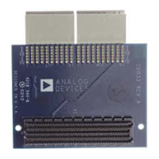
Page 45: Evaluation Board Operation
AD9776/AD9778/AD9779 EVALUATION BOARD OPERATION The AD977x evaluation board is designed to optimize the DAC The evaluation board comes with software that allows the user performance and the speed of the digital interface while to program the SPI port. Via the SPI port, the devices can be remaining user friendly. - Page 46 AD9776/AD9778/AD9779 1. SET INTEROPOLATION RATE 2. SET INTEROPOLATION FILTER MODE 3. SET INPUT DATA FORMAT 4. SET DATACLK POLARITY TO MATCH INPUT TIMING Figure 100. SPI Port Software Window The default settings for the evaluation board allow the user to...
-
Page 47: Modifying The Evaluation Board To Use The Ad8349 On-Board Quadrature Modulator
MODIFYING THE EVALUATION BOARD TO USE THE AD8349 ON-BOARD QUADRATURE MODULATOR The evaluation board contains an Analog Devices AD8349 quadrature modulator. The AD977x and AD8349 provide an easy-to-interface DAC/modulator combination that can be easily evaluated on the evaluation board. To route the DAC... -
Page 48: Evaluation Board Schematics
AD9776/AD9778/AD9779 EVALUATION BOARD SCHEMATICS Rev. 0 | Page 48 of 56 3U63... - Page 49 AD9776/AD9778/AD9779 50Ω JP16 0Ω JP17 0Ω ADTL1-12 ADTL1-12 TC1-1T TC1-1T 50Ω 50Ω JP14 0Ω JP15 0Ω TC1-1T TC1-1T ADTL1-12 ADTL1-12 50Ω DGND;5 DPWR33 0.1μF 0.1μF 0.1μF 0.1μF 10Ω 0.1μF 0.1μF 6.3V 0.1μF 0.1μF 10μF VOLT VOLT 4.7μF 4.7μF 1KΩ 1KΩ...
- Page 50 AD9776/AD9778/AD9779 20Ω 2.1pF 0.1μF 17.2pF 17.2pF 40Ω 150Ω AUX1_N 55nH JP13 150Ω 300Ω 4.5pF AUX1_P 150Ω 17.2pF 55nH 17.2pF 40Ω 147.5Ω 20Ω MODULATED OUTPUT 100pF VDDM 10μF 0.1μF 0.1μF DGND2 DGND2 DGND2 VDDM 1kΩ DGND2 LOCAL OSC OUTPUT 0.1μF 100pF...
- Page 51 AD9776/AD9778/AD9779 SCLK P2D0 P2D1 P2D2 P2D3 P2D4 P2D5 P2D6 P2D7 P2D8 P2D9 P2D10 P2D11 P2D12 P2D13 P2D14 P2D15 P1D0 P1D1 P1D2 P1D3 P1D4 P1D5 P1D6 P1D7 P1D8 P1D9 P1D10 P1D11 P1D12 P1D13 P1D14 P1D15 PKG_TYPE = MOLEX110 PKG_TYPE = MOLEX110...
- Page 52 AD9776/AD9778/AD9779 Figure 108. Evaluation Board, Rev. D, Top Silk Screen Figure 109. Evaluation Board, Rev. D, Top Layer Rev. 0 | Page 52 of 56...
- Page 53 AD9776/AD9778/AD9779 Figure 110. Evaluation Board, Rev. D, Layer 2 Figure 111. Evaluation Board, Rev. D, Layer 3 Rev. 0 | Page 53 of 56...
- Page 54 AD9776/AD9778/AD9779 Figure 112. Evaluation Board, Rev. D, Bottom Layer Figure 113. Evaluation Board, Rev. D, Bottom Silkscreen Rev. 0 | Page 54 of 56...
-
Page 55: Outline Dimensions
AD9776/AD9778/AD9779 OUTLINE DIMENSIONS 16.00 BSC SQ 1.20 0.75 0.60 14.00 BSC SQ 0.45 PIN 1 9.50 SQ TOP VIEW EXPOSED (PINS DOWN) BOTTOM VIEW 0° MIN 1.05 (PINS UP) 0.20 1.00 0.09 0.95 7° 3.5° 0.50 BSC 0.27 VIEW A 0.15... - Page 56 AD9776/AD9778/AD9779 NOTES © 2005 Analog Devices, Inc. All rights reserved. Trademarks and registered trademarks are the property of their respective owners. D05361-0-7/05(0) Rev. 0 | Page 56 of 56...
Need help?
Do you have a question about the AD9776 and is the answer not in the manual?
Questions and answers