Table of Contents
Advertisement
Quick Links
One Technology Way · P.O. Box 9106 · Norwood, MA 02062-9106 · Tel: 781.329.4700 · Fax: 781.461.3113 ·
www.analog.com
EVALUATING THE AD9683/AD6677
ANALOG-TO-DIGITAL CONVERTERS
Preface
This user guide describes the
AD9683
and
AD6677
evaluation boards; AD9683-170EBZ,
AD9683-250EBZ, and AD6677EBZ; which provide all of the support circuitry required to operate these
parts in their various modes and configurations. The application software used to interface with the
devices is also described.
The
AD9683
and
AD6677
data sheets provide additional information and should be consulted when
using the evaluation board. All documents and software tools are available at
www.analog.com/hsadcevalboard. For additional information or questions, send an email to
highspeed.converters@analog.com.
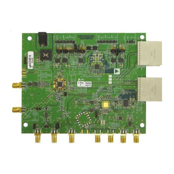
Typical Measurement Setup
Rev 05 Jun 2013 16:37 | Page 1
Advertisement
Table of Contents

Related Manuals for Analog Devices AD9683


Summary of Contents for Analog Devices AD9683
- Page 1 This user guide describes the AD9683 AD6677 evaluation boards; AD9683-170EBZ, AD9683-250EBZ, and AD6677EBZ; which provide all of the support circuitry required to operate these parts in their various modes and configurations. The application software used to interface with the devices is also described. AD9683...
-
Page 2: Helpful Documents
AD9683-170EBZ, AD9683-250EBZ, or AD6677EBZ board HSC-ADC-EVALDZ FPGA-based data capture kit Getting Started This section provides quick start procedures for using the AD9683-170EBZ, AD9683-250EBZ, or AD6677EBZ board. Both the default and optional settings are described. Rev 05 Jun 2013 16:37 | Page 2... -
Page 3: Evaluation Board Hardware
Use a 1 m, shielded, RG-58, 50 Ω coaxial cable to connect the signal generator. For best results, use a narrow-band, band-pass filter with 50 Ω terminations and an appropriate center frequency. (Analog Devices, Inc., uses TTE, Allen Avionics, and K&L band-pass filters.) -
Page 4: Input Signals
Inc. Connect the filters directly to the evaluation board. If an external clock source is used, it should also be supplied with a clean signal generator as previously specified. Analog Devices evaluation boards typically can accept ~2.8 V p-p or 13 dBm sine wave input for the clock. -
Page 5: Evaluation Board Circuitry
FPGA (for the JESD204B link) on the HSC-ADC-EVALDZ. Figure 2. Default Jumper Connections for AD9683-170EBZ/AD9683-250EBZ/AD6677EBZ Board Evaluation Board Circuitry This section explains the default and optional settings or modes allowed on the AD9683-170EBZ, AD9683-250EBZ, and AD96677EBZ boards. Rev 05 Jun 2013 16:37 | Page 5... -
Page 6: Analog Input
The analog input on the evaluation board is set up for a double balun-coupled analog input with a 50 Ω impedance. The default analog input configuration supports analog input frequencies of up to ~400 MHz. For additional information on recommended input networks, see the AD9683 AD6677 data sheets. -
Page 7: How To Use The Software For Testing
AD9683 AD6677 are also equipped with a single-ended RF Clock input that can receive input frequencies from 625 MHz up to 1.5 GHz. This feature must be enabled via SPI and a clock of appropriate frequency must be connected to the RF_CLK SMA connector. The RF Clock circuitry within... - Page 8 Click the Settings button on the ADC Data Capture block. In the pop-up window select the Capture Board tab. Select the checkbox Poll Full Flag. This must be checked in order to get data capture from the AD9683 AD6677 (see Figure 5).
- Page 9 Figure 5. VisualAnalog ADC Data Capture Settings To change features to settings other than the default settings, click the Expand Display button, located in the bottom right corner of the window (see Figure 6), to see what is shown in Figure 7. Change the features and capture settings by consulting the detailed instructions in the AN-905 Application...
-
Page 10: Evaluation And Test
Figure 7. VisualAnalog, Main Window, Expanded Display Evaluation And Test Setting up the SPI Controller Software After the ADC data capture board setup is complete, set up the SPI controller software using the following procedure: Open the SPI controller software by going to the Start menu or by double-clicking the SPIController software desktop icon. - Page 11 Figure 8. SPI Controller, CHIP ID(1) Box Click the New DUT button in the SPIController window (see Figure 9). Rev 05 Jun 2013 16:37 | Page 11...
- Page 12 Figure 9. SPI Controller, New DUT Button In the ADCBase 0 tab of the SPIController window, find the CLOCK DIVIDE(B) box (see Figure 10). If using the clock divider, use the drop-down box to select the correct clock divide ratio, if necessary.
- Page 13 Figure 10. SPI Controller, ADCBase0 Note that other settings can be changed on the ADCBase0 tab (see Figure 10) and the ADCBase1 and ADCBase2 tabs (see Figures 11 and 12) to set up the part in the desired mode. The ADCBase0 tab settings affect ADC settings, whereas the settings on the ADCBase1 and ADCBase2 tabs affect the JESD204B link settings.
- Page 14 Figure 11. SPI Controller, Example ADCBase1 Page Rev 05 Jun 2013 16:37 | Page 14...
-
Page 15: Adjusting The Amplitude Of The Input Signal
Figure 12. SPI Controller, Example ADCBase1 Page Click the Run button in the VisualAnalog toolbar (see Figure 13). Figure 13. Run Button (Encircled in Red) in VisualAnalog Toolbar, Collapsed Display Adjusting the Amplitude of the Input Signal The next step is to adjust the amplitude of the input signal for each channel as follows: Adjust the amplitude of the input signal so that the fundamental is at the desired level. -
Page 16: Troubleshooting Tips
(see Figure 14). Figure 14. Graph Window of VisualAnalog Repeat this procedure for Channel B, Channel C, and Channel D. Click the disk icon within the VisualAnalog Graph - AD9253 FFT window to save the performance plot data as a .csv formatted file. See Figure 15 for an example. Figure 15. - Page 17 Make sure that all power and USB connections are secure. Make sure that the Poll Full Flag checkbox is checked under ADC Capture Settings in Visual Analog. © Analog Devices, Inc. All rights reserved. Trademarks and registered trademarks are the property of their respective owners. www.analog.com...
Need help?
Do you have a question about the AD9683 and is the answer not in the manual?
Questions and answers