Table of Contents
Advertisement
Quick Links
One Technology Way · P.O. Box 9106 · Norwood, MA 02062-9106 · Tel: 781.329.4700 · Fax: 781.461.3113 ·
www.analog.com
EVALUATING THE AD9653/AD9253/AD9633
ANALOG-TO-DIGITAL CONVERTERS
Preface
This user guide describes the AD9653,
AD9253
and
AD9633
evaluation boards, AD9653-125EBZ,
AD9253-125EBZ
and AD9633-125EBZ, which provide all of the support circuitry required to operate
these parts in their various modes and configurations. The application software used to interface with
the devices is also described.
The
AD9653 AD9253
and
AD9633
data sheets provide additional information and should be consulted
when using the evaluation board. All documents and software tools are available at
www.analog.com/hsadcevalboard. For additional information or questions, send an email to
highspeed.converters@analog.com.
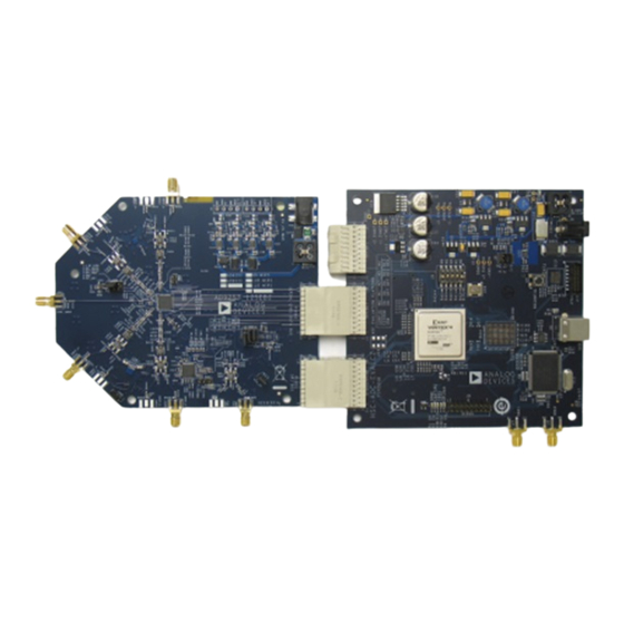
Typical Measurement Setup
Figure 1. Evaluation Board Connection—AD9653-125EBZ,
AD9253-125EBZ
or
AD9633-125EBZ
(on Left)
and
HSC-ADC-EVALCZ
(on Right)
Rev 13 May 2013 17:57 | Page 1
Advertisement
Table of Contents

Related Manuals for Analog Devices AD9653


Summary of Contents for Analog Devices AD9653
- Page 1 One Technology Way · P.O. Box 9106 · Norwood, MA 02062-9106 · Tel: 781.329.4700 · Fax: 781.461.3113 · www.analog.com EVALUATING THE AD9653/AD9253/AD9633 ANALOG-TO-DIGITAL CONVERTERS Preface This user guide describes the AD9653, AD9253 AD9633 evaluation boards, AD9653-125EBZ, AD9253-125EBZ and AD9633-125EBZ, which provide all of the support circuitry required to operate these parts in their various modes and configurations.
-
Page 2: Helpful Documents
AD9653-125EBZ, AD9253-125EBZ AD9633-125EBZ board HSC-ADC-EVALCZ FPGA-based data capture kit Getting Started This section provides quick start procedures for using the AD9653-125EBZ, AD9253-125EBZ AD9633-125EBZ board. Both the default and optional settings are described. Rev 13 May 2013 17:57 | Page 2... -
Page 3: Evaluation Board Hardware
A and/or B channel(s). Use a 1 m, shielded, RG-58, 50 Ω coaxial cable to connect the signal generator. For best results, use a narrow-band, band-pass filter with 50 Ω terminations and an appropriate center frequency. (Analog Devices, Inc., uses TTE, Allen Avionics, and K&L band-pass filters.) -
Page 4: Input Signals
Inc. Connect the filters directly to the evaluation board. If an external clock source is used, it should also be supplied with a clean signal generator as previously specified. Analog Devices evaluation boards typically can accept ~2.8 V p-p or 13 dBm sine wave input for the clock. -
Page 5: Evaluation Board Circuitry
To apply a reference voltage from an external off-board source, connect Pin 2 (DUT_SENSE) to Pin 1 (AVDD) and apply the reference voltage to Pin 4 (DUT_VREF). The AD9653 can accommodate reference voltages from 1.0 V to 1.3 V; the AD9253 and AD9633 reference voltage is specified to be 1.0 V. -
Page 6: Analog Input
Pin 6 on Header J202. Alternatively, if an external off-board reference is desired, connect Pin 2 to Pin1 on Header J202 and apply the reference voltage directly to Pin 4 of Header J202. The AD9653 can accommodate reference voltages from 1.0 V to 1.3 V; the AD9253 and AD9633 reference voltage is specified to be 1.0 V. -
Page 7: Modes Of Operation
Output Mode Resulting D0±x and D1±x Normal Operation 10 kΩ to AGND Normal operation AVDD 1000 0000 0000 0000 Additional information on the lane modes is provided in the AD9653, AD9253 AD9633 data sheets. Rev 13 May 2013 17:57 | Page 7... -
Page 8: Default Mode
Default Mode To operate the device under test (DUT) using the SPI, follow the jumper settings for J302 as shown in Table 1. How To Use The Software For Testing Setting up the ADC Data Capture After configuring the board, set up the ADC data capture using the following steps: Open VisualAnalog on the connected PC. -
Page 9: Evaluation And Test
located on the bottom right corner of the window (see Figure 5), to see what is shown in Figure 6. Change the features and capture settings by consulting the detailed instructions in the AN-905 Application Note, VisualAnalog Converter Evaluation Tool Version 1.0 User Manual. After the changes are made to the capture settings, click the Collapse Display button. - Page 10 Figure 7. SPI Controller, CHIP ID(1) Click the New DUT button in the SPIController window (see Figure 8) Figure 8. SPI Controller, New DUT Button In the ADCBase 0 tab of the SPIController window, find the CLOCK DIVIDE(B) box (see Figure 9).
-
Page 11: Adjusting The Amplitude Of The Input Signal
via SPI. Figure 9. SPI Controller, CLOCK DIVIDE(B) Box Note that other settings can be changed on the ADCBase 0 tab (see Figure 9) and the ADC A, ADC B, ADC C, and ADC D tabs (see Figure 10) to set up the part in the desired mode. The ADCBase 0 tab settings affect the entire part, whereas the settings on the ADC A, ADC B, ADC C, and ADC D tabs affect the selected channel only. -
Page 12: Troubleshooting Tips
Adjust the amplitude of the input signal so that the fundamental is at the desired level. Examine the Fund Power reading in the left panel of the VisualAnalog Graph - AD9253 FFT window (see Figure 12). Figure 12. Graph Window of VisualAnalog Repeat this procedure for Channel B, Channel C, and Channel D. - Page 13 Probe the DCO signal at P1002 (Pin A10 and/or Pin B10) on the evaluation board, and confirm that a clock signal is present at the ADC sampling rate. © Analog Devices, Inc. All rights reserved. Trademarks and registered trademarks are the property of their respective owners.
Need help?
Do you have a question about the AD9653 and is the answer not in the manual?
Questions and answers