Table of Contents
Advertisement
Quick Links
AD9739A Native FMC Card / Xilinx Reference Designs [Analog Devices Wiki]
world leader in high performance signal processing
Login
Analog Devices Wiki
Enter keywords or part # Search Wiki
Resources and Tools
■
Evaluation Boards & Kits
■
FPGA Reference Designs
■
Quick Start Guides
■
Tools & Software
■
Wiki Help
■
Help
■
About Wiki
■
Playground
■
Wiki Site Map
■
Design Support
■
EngineerZone
■
Circuits from the Lab
■
Product Selection Guides
■
[http://www.analog.com/en/content/psearch_landing/fca.html]
ReadView Source|History
Print | Export Open Office | PDF | RSS
This version (
25 Apr 2012 13:17
AD9739A Native FMC Card / Xilinx Reference Designs
Introduction
The
AD9739A
[http://www.analog.com/AD9739A]
capable of synthesizing wideband signals with up to 1.25GHz of bandwidth. This reference design
includes a single tone sine generator (DDS) and allows programming the device and monitoring
it's internal status registers. It also programs the
clock chip which can generate a 1.6GHz to 2.5GHz clock for the AD9739A from the on-board
25MHz crystal. An alternate clock path using an
is available for driving the clock externally.
http://wiki.analog.com/resources/fpga/xilinx/fmc/ad9739a?force_rev=1
[http://ez.analog.com/]
[http://www.analog.com/circuits]
) is a Draft.
is a 14-bit, 2.5 GSPS high performance RF DAC
ADF4350
[http://www.analog.com/ADF4350]
ADCLK914
[http://www.analog.com/ADCLK914]
Page 1 of 12
5/22/2012
Advertisement
Table of Contents

Related Manuals for Analog Devices AD9739A


Summary of Contents for Analog Devices AD9739A
- Page 1 (DDS) and allows programming the device and monitoring it's internal status registers. It also programs the ADF4350 [http://www.analog.com/ADF4350] clock chip which can generate a 1.6GHz to 2.5GHz clock for the AD9739A from the on-board 25MHz crystal. An alternate clock path using an ADCLK914 [http://www.analog.com/ADCLK914] is available for driving the clock externally.
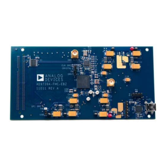
- Page 2 AD9739A Native FMC Card / Xilinx Reference Designs [Analog Devices Wiki] Page 2 of 12 HW Platform(s): Virtex-6 ML605 (Xilinx) [http://www.xilinx.com/products/boards-and-kits/EK-V6- , Kintex-7 KC705 (Xilinx) ML605-G.htm] [http://www.xilinx.com/products/boards-and-kits/EK-K7-KC705- or Virtex-7 VC707 (Xilinx) G.htm] [http://www.xilinx.com/products/boards-and-kits/EK-V7-VC707- AD9739A-FMC-EBZ G.htm] [http://www.analog.com/en/digital-to-analog-converters/da- (ADI) converters/ad9739a/products/EVAL-AD9739A/eb.html] System: Microblaze, AXI, UART This reference design is based on KC705 IES (rev.C) board.
-
Page 3: Required Hardware
SMA jack (OUT/J1). This quick start program uses a 2.5GHz DAC clock and generates a 300MHz tone. Adjust your spectrum analyzer accordingly. On the AD9739A-FMC board, ensure that the SPI source jumper (SPI SRC/P2) is set http://wiki.analog.com/resources/fpga/xilinx/fmc/ad9739a?force_rev=1... - Page 4 FMC and the clock source jumper (CLK SRC/P3) is set to crystal (XTAL). The USB connection on the AD9739A-FMC-EBZ and the SMA Clock Input (SMA CLKIN/J3) are not used in this example. After the hardware setup, turn the power on to the ML605.
- Page 5 TV (CATV) system. It is employed by many cable television operators to provide data access over their existing infrastructure. It has many specification, certification, and testing criteria. Below are example ACLR and spur measurements for this card with the AD9739A running at 2.5GHz with carrier(s) centered at 980MHz.
-
Page 6: Using The Reference Design
The DDS consists of a Xilinx DDS IP core and a DDR based data generator. The core generates 6 samples at every fDAC/3 clock cycles for each port of AD9739A. The frequency of the DDS as well as the LUT entries are programmable via SDK. -
Page 7: Hardware Reference
The above list is partial and only lists the key parameters for reference. Hardware Reference There are several hardware options available on the AD9739A-FMC-EBZ: Clock Selection Two clock paths are availabe to drive the clock input on the AD9739A-FMC-EBZ. The factory default option connects the ADF4350 to the AD9739A [http://www.analog.com/ADF4350]... - Page 8 The software for controlling the ADF4350 clock chip is installed to the start menu at Start > Programs > Analog Devices > AD9739A > ADF4350 SPI for AD9739A-FMC-EBZ. Once open, select File…Open Setup File. Browse for the file 2_5GHz for AD9739A.ini, which is located in Analog Devices\HSDAC\AD9739A inside your Program Files directory (usually C:\Program Files or C:\Program Files(x86)).
- Page 9 AD9739A Native FMC Card / Xilinx Reference Designs [Analog Devices Wiki] Page 9 of 12 Cross Control CLKP Offset Setting: Register 0x24 Bits 0-3 CLKP Direction Bit: Register 0x24 Bit 4 CLKP Offset Setting: Register 0x25 Bits 0-3 CLKP Direction Bit: Register 0x25 Bit 4 Damp: Register 0x25 Bits...
- Page 10 Below is a list of hardware, IP Cores, or reference designs. While this content is believed to be reliable, many have not been validated, verified or reviewed by Analog Devices. These boards/platforms may or may not be suitable for end product integration or development, and may not meet datasheet specifications.
- Page 11 AD9739A Native FMC Card / Xilinx Reference Designs [Analog Devices Wiki] Page 11 of 12 designed or reviewed by Analog Devices, care should be taken to ensure that these will meet your needs before purchase. While ADI will always provide chip level support on EngineerZone™...
- Page 12 AD9739A Native FMC Card / Xilinx Reference Designs [Analog Devices Wiki] Page 12 of 12 Careers Contact ADI | About ADI Investor Relations News Room | About This Site Wiki Sitemap | eNewsletters © 1995 - 2012 Analog Devices, Inc. and other contributors.
Need help?
Do you have a question about the AD9739A and is the answer not in the manual?
Questions and answers