Table of Contents
Advertisement
Quick Links
One Technology Way · P.O. Box 9106 · Norwood, MA 02062-9106 · Tel: 781.329.4700 · Fax: 781.461.3113 ·
EVALUATING THE
AD9266/AD9649/AD9629/AD9609
ANALOG-TO-DIGITAL CONVERTERS
Preface
This QuickStart user guide describes the evaluation boards, AD9266-80EBZ, AD9649-80EBZ,
AD9629-80EBZ, and
products: AD9266, AD9649, AD9629, and AD9609. These evaluation boards provide the support
circuitry required to operate these devices in their various modes and configurations. The application
software used to interface with the devices is also described.
The
AD9266
, AD9649, AD9629, and
be consulted when using the evaluation board. All documents and software tools are available at
www.analog.com/hsadcevalboard. For additional information or questions, send an email to
highspeed.converters@analog.com.
Note that, though the 80 MSPS speed grade ADCs and boards are referred to in this document, this
user guide is applicable to the other speed grades, as well.
The
AD9266/AD9649/AD9629/AD9609
ADCs. Additional application information can be found in the
ADCs of this
family.
Typical Measurement Setup
AD9609-80EBZ
that are used to evaluate the following Analog Devices, Inc.,
AD9609
share ADC core characteristics with the
Rev 03 Jun 2015 18:39 | Page 1
data sheets provide additional information and should
Evaluation Board User Guide for Dual
www.analog.com
AD9269
family of dual
Advertisement
Table of Contents

Subscribe to Our Youtube Channel
Related Manuals for Analog Devices AD9266


Summary of Contents for Analog Devices AD9266
- Page 1 AD9609-80EBZ that are used to evaluate the following Analog Devices, Inc., products: AD9266, AD9649, AD9629, and AD9609. These evaluation boards provide the support circuitry required to operate these devices in their various modes and configurations. The application software used to interface with the devices is also described.
-
Page 2: Helpful Documents
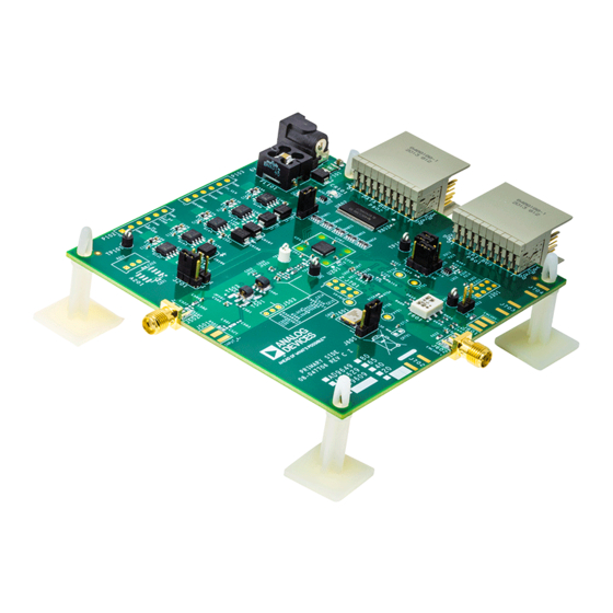
Figure 1. Evaluation Board Connection—AD9266-80EBZ/AD9649-80EBZ/AD9629-80EBZ/ AD9609-80EBZ (on Left) and HSC-ADC-EVALCZ (on Right) Helpful Documents AD9266, AD9649, AD9629, AD9609 data sheet HSC-ADC-EVALC data sheet AN-905 Application Note, VisualAnalog Converter Evaluation Tool Version 1.0 User Manual AN-878 Application Note, High Speed ADC SPI Control Software... -
Page 3: Getting Started
Configuring the Board Before using the software for testing, configure the evaluation board as follows: Connect the evaluation board to the data capture board, as shown in Figure 1. The AD9266, AD9649, AD9629, and AD9609 are all pin compatible and use the same evaluation board. -
Page 4: Power Supplies
(see the Specifications section in the ADC data sheet). When connecting the analog input source, use of a multipole, narrow-band band-pass filter with 50 Ω terminations is recommended. Analog Devices uses band-pass filters from TTE and K&L Microwave, Inc. Connect the filters directly to the evaluation board. -
Page 5: Output Signals
To apply a reference voltage from an external off-board source, connect J201 Pin 2 (DUT_SENSE) to J201 Pin 1 (1.8V_DUT_AVDD) and apply the reference voltage to J202 Pin 2 (DUT_VREF). The reference voltage is specified at 1.0 V for the AD9266, AD9649, AD9629, and AD9609. -
Page 6: Evaluation Board Circuitry
Figure 2. Default Jumper Connections for AD9266-80EBZ/AD9649-80EBZ/AD9629-80EBZ/ AD9609-80EBZ Board Evaluation Board Circuitry This section explains the default and optional ADC settings or modes allowed on the AD9266-80EBZ and the AD9649-80EBZ boards. Power Connect the switching power supply that is supplied in the evaluation kit between a rated 100 V ac to 240 V ac, 47 Hz to 63 Hz wall outlet and to P101. -
Page 7: Modes Of Operation
50 Ω terminated and ac-coupled to handle single-ended sinusoidal inputs. The transformer converts the single-ended input to a differential signal that is clipped by CR601 before entering the ADC clock inputs. The AD9266,AD9649,AD9629, and AD9609 ADCs are equipped with an internal 8:1 clock divider to facilitate use with higher frequency clocks. -
Page 8: Default Mode
Note that the settings in Table 2 and Table 3 apply only when CSB is tied high (J302 Pin 8 has no jumper) at power up. Additional information on the standalone (pin) mode is provided in the AD9266, AD9649, AD9629, and AD9609 data sheets. - Page 9 example). Figure 3. VisualAnalog, New Canvas Window After the template is selected, a message might appear asking if the default configuration can be used to program the FPGA (see Figure 4). If this message appears, click Yes, and the window closes.
-
Page 10: Evaluation And Test
Figure 5. VisualAnalog Window Toolbar, Collapsed Display Figure 6. VisualAnalog, Main Window Expanded Display Evaluation And Test Setting up the SPI Controller Software After the ADC data capture board setup is complete, set up the SPI controller software using the following procedure: Open the SPI controller software by going to the Start menu or by double-clicking the SPIController software desktop icon. - Page 11 controller configuration file is loaded (see Figure 7). Figure 7. SPI Controller, CHIP ID(1) Box Click the New DUT button in the SPIController window (see Figure 8). Rev 03 Jun 2015 18:39 | Page 11...
- Page 12 Figure 8. SPI Controller, New DUT Button In the ADCBase 0 tab of the SPIController window, find the CLOCK DIVIDE(B) box (see Figure 9), and the MODES(8) box (see Figure 9). If using the clock divider, use the drop-down menu to select the correct clock divide ratio, as desired.
-
Page 13: Adjusting The Amplitude Of The Input Signal
The next step is to adjust the amplitude of the input signal as follows: Adjust the amplitude of the input signal so that the fundamental is at the desired level. Examine the Fund Power reading in the left panel of the VisualAnalog Graph - AD9266 FFT window (see Figure 12). -
Page 14: Troubleshooting Tips
Figure 12. Graph Window of VisualAnalog Click the floppy disk icon within the VisualAnalog Graph - AD9266 FFT window to save the performance data as a .csv formatted file for plotting or analysis. Troubleshooting Tips Lack of SPI communication causes difficulty in configuring the ADC. - Page 15 Data Capture block in VisualAnalog. Then, select the FPGA tab and verify that the proper FPGA bin file is selected for the device. © Analog Devices, Inc. All rights reserved. Trademarks and registered trademarks are the property of their respective owners.
Need help?
Do you have a question about the AD9266 and is the answer not in the manual?
Questions and answers