Table of Contents
Advertisement
Quick Links
Preliminary Technical Data
FEATURES
• 1.8/3.3 V Single Supply Operation
• Low power: 950mW (I
OUTFS
Interpolation
• DNL = ± 1.5 LSB, INL = ± 5.0 LSB
• SFDR =82 dBc to f
= 100 MHz
OUT
• ACLR = 87 dBc @ 80 MHz IF
• CMOS data interface with Autotracking Input Timing
• Analog Output: Adjustable 10-30mA (RL=25 Ω to 50 Ω)
• 100-lead Exposed Paddle TQFP Package
• Multiple Chip Synchronization Interface
• 84dB Digital Interpolation Filter Stopband Attenuation
• Digital Inverse Sinc Filter
APPLICATIONS
• Wireless Infrastructure
Direct Conversion
Transmit Diversity
• Wideband Communications Systems:
Point-to-Point Wireless, LMDS
PRODUCT DESCRIPTION
The AD9779 is a dual 16-bit high performance, high frequency
FUNCTIONAL BLOCK DIAGRAM
SYNC_O
SYNC_I
DATACLK_OUT
P1D[15:0]
P2D[15:0]
Rev. PrD
Information furnished by Analog Devices is believed to be accurate and reliable.
However, no responsibility is assumed by Analog Devices for its use, nor for any
infringements of patents or other rights of third parties that may result from its use.
Specifications subject to change without notice. No license is granted by implication
or otherwise under any patent or patent rights of Analog Devices. Trademarks and
registered trademarks are the property of their respective owners.
= 20 mA; f
= 1 GSPS, 4×
DAC
Delay Line
Delay Line
Data
Assembler
I Latch
2X
2X
Q Latch
2X
2X
Serial
Peripheral
Interface
Figure 1 Functional Block Diagram
DAC that provides a sample rate of 1 GSPS, permitting multi
carrier generation up to its Nyquist frequency. It includes features
optimized for direct conversion transmit applications, including
complex digital modulation and gain and offset compensation. The
DAC outputs are optimized to interface seamlessly with analog
quadrature modulators such as the AD8349. A serial peripheral
interface (SPI) provides for programming many internal
parameters and also enables read-back of status registers. The
output current can be programmed over a range of 10mA to 30mA.
The AD9779 is manufactured on an advanced 0.18µm CMOS
process and operates from 1.8V and 3.3V supplies for a total power
consumption of 950mW. It is supplied in a 100-lead QFP package.
PRODUCT HIGHLIGHTS
Ultra-low noise and Intermodulation Distortion (IMD) enable
high quality synthesis of wideband signals from baseband to high
intermediate frequencies.
Single-ended CMOS interface supports a maximum input rate of
300 MSPS with 1x interpolation.
Manufactured on a CMOS process, the AD9779 uses a proprietary
switching technique that enhances dynamic performance.
The current outputs of the AD9779 can be easily configured for
various single-ended or differential circuit topologies.
Clock Generation/Distribution
2X
n * Fdac/8
Complex
n = 1, 2, 3... 7
Modulator
2X
Digital Controller
10
10
Power-On
Reset
10
10
One Technology Way, P.O. Box 9106, Norwood, MA 02062-9106, U.S.A.
Tel: 781.329.4700
Fax: 781.326.8703
Dual 16-Bit, 1.0 GSPS
D/A Converter
Clock
CLK+
Multiplier
CLK-
2X/4X/8X
IOUT1_P
-1
Sinc
16-Bit
IDAC
IOUT1_N
IOUT2_P
16-Bit
QDAC
-1
Sinc
IOUT2_N
Gain
Gain
VREF
Reference
& Bias
RSET
AUX1_P
Offset
AUX1_N
AUX2_P
Offset
AUX2_N
© 2005 Analog Devices, Inc. All rights reserved.
AD9779
www.analog.com
Advertisement
Table of Contents

Related Manuals for Analog Devices AD9779


Summary of Contents for Analog Devices AD9779
- Page 1 Information furnished by Analog Devices is believed to be accurate and reliable. However, no responsibility is assumed by Analog Devices for its use, nor for any infringements of patents or other rights of third parties that may result from its use.
-
Page 2: Table Of Contents
AD9779 Preliminary Technical Data TABLE OF CONTENTS Specifications....................3 Instruction Byte .................12 DC SPECIFICATIONS ..............3 Serial Interface Port Pin Descriptions ..........12 DIGITAL SPECIFICATIONS............4 MSB/LSB Transfers ................13 AC SPECIFICATIONS...............4 Notes on Serial Port Operation ............13 Pin Function Descriptions ..............5 SPI Register Map ................14 Pin Configuration..................6... -
Page 3: Specifications
Preliminary Technical Data AD9779 SPECIFICATIONS DC SPECIFICATIONS (VDD33 = 3.3 V, VDD18 = 1.8 V, MAXIMUM SAMPLE RATE, UNLESS OTHERWISE NOTED) Parameter Temp Test Level Unit RESOLUTION Bits ± 1.5 Integral Nonlinearity (DNL) ACCURACY ± 5 Differential Nonlinearity (INL) ± TBD... -
Page 4: Digital Specifications
AD9779 Preliminary Technical Data DIGITAL SPECIFICATIONS (VDD33 = 3.3 V, VDD18 = 1.8 V, MAXIMUM SAMPLE RATE, UNLESS OTHERWISE NOTED) Parameter Temp Test Level Unit Differential peak-to-peak Voltage DAC CLOCK INPUT Common Mode Voltage (CLK+, CLK-) Maximum Clock Rate GSPS... -
Page 5: Pin Function Descriptions
Preliminary Technical Data AD9779 PIN FUNCTION DESCRIPTIONS Name Description Name Description VDDC18 1.8 V Clock Supply P2D<6> Port 2 Data Input D6 VDDC18 1.8 V Clock Supply P2D<5> Port 2 Data Input D5 VSSC Clock Common VDDD18 1.8 V Digital Supply... -
Page 6: Pin Configuration
AD9779 Preliminary Technical Data PIN CONFIGURATION VDDC18 I120 VDDC18 VREF Analog Domain VSSC IPTAT VSSC CLK+ CLK- RESET Digital Domain VSSC SPI_CSB VSSC SPI_CLK VDDC18 SPI_SDI VDDC18 SPI_SDO VSSC PLL_LOCK VSSC VSSD AD9779 SYNC_I+ SYNC_O+ SYNC_I- SYNC_O- VSSD VDDD33 VDDD33 VDDD18 P1D<15>... -
Page 7: Interpolation Filter Coefficients
Preliminary Technical Data AD9779 INTERPOLATION FILTER COEFFICIENTS Table 7: Halfband Filter 3 Table 5: Halfband Filter 1 Lower Upper Integer Lower Upper Integer Coefficient Coefficient Value Coefficient Coefficient Value H(1) H(15) H(1) H(55) H(2) H(14) H(2) H(54) H(3) H(13) H(3) -
Page 8: Interpolation Filter Response Curves
AD9779 Preliminary Technical Data INTERPOLATION FILTER RESPONSE CURVES -100 Figure 3. AD9779 2x Interpolation, Low Pass Response to ±4x Input Data Rate (Dotted Lines Indicate 1dBRoll-Off) -100 Figure 4. AD9779 4x Interpolation, Low Pass Response to ±4x Input Data Rate (Dotted Lines Indicate 1dBRoll-Off) -100 Figure 5.AD9779 8x Interpolation, Low Pass Response to... -
Page 9: Characterization Data
D ATA 8192 16384 24576 32768 40960 49152 57344 65536 Code Fout - MHz Figure 6. AD9779 Typical INL Figure 9. SFDR vs. F , 2x Interpolation =125MSPS D ATA =100MSPS D ATA =200MSPS D ATA =150MSPS D ATA -0.5... - Page 10 AD9779 Preliminary Technical Data 100.0 =200MSPS D ATA 90.0 100MSPS 80.0 112.5MSPS 75MSPS =160MSPS D ATA 50MSPS 70.0 =62.5MSPS D ATA 60.0 50.0 Fout - MHz Fout - MHz Figure 15. Third Order IMD vs. F , 8x Interpolation Figure 12. Third Order IMD vs. F , 1x Interpolation 100.0...
- Page 11 Preliminary Technical Data AD9779 8x Interpolation =122.88MSPS D ATA 4x Interpolation 4x Interpolation, 8x Interpolation, Zero Stuffing Zero Stuffing 2x Interpolation, Zero Stuffing =61.44MSPS D ATA 2x Interpolation 1x Interpolation, Zero Stuffing 1x Interpolation 100 120 140 160 180 200 220 240 260 280 300 Fout - M Hz Figure 18.
-
Page 12: General Description
SCLK’s maximum frequency is 20 MHz. All data input register address for the first byte of the data transfer. The first eight to the AD9779 is registered on the rising edge of SCLK. All data is SCLK rising edges of each communication cycle are used to write driven out of the AD9779 on the falling edge of SCLK. -
Page 13: Msb/Lsb Transfers
SDO—Serial Data Out. Data is read from this pin for protocols SCLK that use separate lines for transmitting and receiving data. In the case where the AD9779 operates in a single bidirectional I/O mode, R/W N0 N1 A0 A1 A2 A3... -
Page 14: Spi Register Map
AD9779 Preliminary Technical Data SPI Register Map Register Address Bit 7 Bit 6 Bit 5 Bit 4 Bit 3 Bit 2 Bit 1 Bit 0 Default Name Comm SDIO LSB,MSB First Software Power Auto PLL Lock Register Bidirectional Reset Down... - Page 15 Preliminary Technical Data AD9779 Aux 2 DAC Auxiliary DAC2 Data <7:0> Control Register Auxiliary Auxiliary Auxiliary Auxiliary DAC2 Data DAC2 Sign DAC2 DAC2 Power <9:8> Current Down Direction Cross Updel <7:0> Cross Cross Dndel <7:0> Register Cross Clock Divide <3:0>...
- Page 16 AD9779 Preliminary Technical Data Register (hex) Bits Name Function Default SDIO Bidirectional 0: Use SDIO pin as input data only 1: Use SDIO as both input and output data Comm Register LSB/MSB First 0: First bit of serial data is MSB of data byte...
- Page 17 Preliminary Technical Data AD9779 Data Delay Error (read only) IRQ Status Chip Synchronization Delay Error (read only) Cross Control Error (read only) Data Delay Error Enable Chip Synchronization Error Enable Cross Control Error Enable PLL Band Select 11001 Table 14 PLL Band and Divide values.
- Page 18 AD9779 Preliminary Technical Data Aux DAC1 Sign 0: Positive 1: Negative Auxiliary DAC1 Control and Data Aux DAC1 0: Source Direction 1: Sink Aux DAC1 Sleep 0: Aux DAC1 on 1: Aux DAC 1 off Aux DAC1 Gain (9:8) MSB slice of 10 bit gain setting word for Aux DAC1...
- Page 19 Preliminary Technical Data AD9779 MISR Enable 0: MISR disabled 1: MISR Enabled MISR Control MISR IQ Select 0: Read back I path signature 1: Read back Q path signature MISR Samples 0: MISR uses short sample period 1: MISR uses long sample period...
- Page 20 AD9779 Preliminary Technical Data Interp. Filter Filter1 mode Filter2 mode Filter3 mode Modulation Nyquist F_low Center F_High (Mode_F1) (Mode_F2) (Mode_F3) Zone Factor Mode Passband <7:6> <5:2> (Freq. Normalized to F DC_odd -0.05 0.05 In 8x interpolation, BW=0.0375- DC_even 0.0125 0.0625 0.1125...
- Page 21 Preliminary Technical Data AD9779 PLL Frequency Band Select 00110 (6) 1525 – 1597 PLL Band Select Value Frequency in MHz 00101 (5) 1560 – 1632 11111 (31) 804 – 850 00100 (4) 1594 – 1667 11110 (30) 827 – 875 00011 (3) 1629 –...
-
Page 22: Internal Reference/Full Scale Current Generation
Internal Reference/Full Scale Current Generation Auxiliary DACs Full scale current on the AD9779 IDAC and QDAC can be set from Two auxiliary DACs are provided on the AD9779. The full scale 10 to 30ma. Initially, the 1.2V bandgap reference is used to set up a output current on these DACs is derived from the 1.2V bandgap... -
Page 23: Internal Pll Clock Multiplier / Clock Distribution
DATACLK out falling edge. Refe rence Clock DATA CLK out Input Data Figure 33. Timing Specifications for AD9779, PLL Enabled, Reference Clock = 1x Input Sample Rate Rev. PrD | Page 23 of 34... - Page 24 Preliminary Technical Data Refe rence Clock DATA CLK out Input Data Figure 34. Timing Specifications for AD9779, PLL Enabled, Reference Clock = 2x Input Sample Rate Refe rence Clock DATA CLK out Input Data Figure 35. Timing Specifications for AD9779, PLL Enabled, Reference Clock = 4x Input Sample Rate...
-
Page 25: Interpolation Filter Architecture
AD9779 Interpolation Filter Architecture The AD9779 can provide up to 8× interpolation or disable the interpolation filters entirely. The coefficients of the low pass filters and the inverse sinc filter are given in Table 5, Table 6, Table 7, and Table 8. - Page 26 The even/odd mode capability allows the passband to be placed anywhere in the DAC Nyquist bandwidth. The AD9779 is a dual DAC with an internal complex modulator -100 built into the interpolating filter response. The modulator can be set to a real or a complex mode by programming register 02h, bit 5.
-
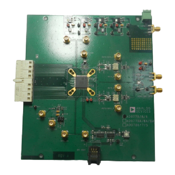
Page 27: Evaluation Board Schematics
Preliminary Technical Data AD9779 EVALUATION BOARD SCHEMATICS Figure 47. AD9779 Eval Board, Rev B , Power Supply Decoupling and SPI Interface Rev. PrD | Page 27 of 34... - Page 28 AD9779 Preliminary Technical Data Figure 48. AD9779 Eval Board, Rev B , Circuitry Local to AD9779 Rev. PrD | Page 28 of 34...
- Page 29 Preliminary Technical Data AD9779 Figure 49. AD9779 Eval Board, RevB , AD8349 Quadrature Modulator Rev. PrD | Page 29 of 34...
- Page 30 AD9779 Preliminary Technical Data Figure 50. AD9779 Eval Board, RevB , DAC Clock Interface Rev. PrD | Page 30 of 34...
- Page 31 Preliminary Technical Data AD9779 Figure 51. AD9779 Eval Board, RevB , Input Port 1, Digital Input Buffers Rev. PrD | Page 31 of 34...
- Page 32 AD9779 Preliminary Technical Data Figure 52. AD9779 Eval Board, RevB , Input Port 2, Digital Input Buffers Rev. PrD | Page 32 of 34...
- Page 33 Preliminary Technical Data AD9779 Outline Dimensions Rev. PrD | Page 33 of 34...
- Page 34 -40°C to +85°C (Ambient) AD9779/PCB 25°C (Ambient) Evaluation Board Table 15: Ordering Guide © 2005 Analog Devices, Inc. All rights reserved. Trademarks and registered trademarks are the property of their respective owners. PR05363–0–1/05(PrD) Rev. PrD | Page 34 of 34...
Need help?
Do you have a question about the AD9779 and is the answer not in the manual?
Questions and answers