Table of Contents
Advertisement
Quick Links
One Technology Way · P.O. Box 9106 · Norwood, MA 02062-9106 · Tel: 781.329.4700 · Fax: 781.461.3113 ·
www.analog.com
EVALUATING THE AD9249
ANALOG-TO-DIGITAL CONVERTER
Preface
This user guide describes the
AD9249
evaluation board AD9249-65EBZ, which provides the support
circuitry required to operate the ADC in its various modes and configurations. The application
software used to interface with the device is also described.
The
AD9249
data sheet provides additional information and should be consulted when using the
evaluation board. All documents and software tools are available at www.analog.com/hsadcevalboard.
For additional information or questions, send an email to highspeed.converters@analog.com.
Typical Measurement Setup
Rev 13 Nov 2013 01:51 | Page 1
Advertisement
Table of Contents

Related Manuals for Analog Devices AD9249


Summary of Contents for Analog Devices AD9249
- Page 1 ANALOG-TO-DIGITAL CONVERTER Preface This user guide describes the AD9249 evaluation board AD9249-65EBZ, which provides the support circuitry required to operate the ADC in its various modes and configurations. The application software used to interface with the device is also described. AD9249 data sheet provides additional information and should be consulted when using the evaluation board.
-
Page 2: Helpful Documents
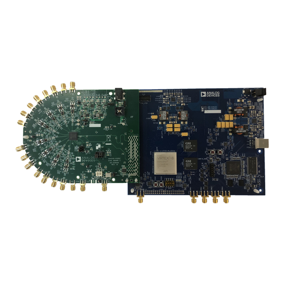
Figure 1. Evaluation Board Connection—AD9249-65EBZ (on Left) and HSC-ADC-EVALDZ (on Right) Features SPI interface for setup and control External, on-board oscillator On-board LDO regulator or switching regulator, needing a single external 6V, 2A dc supply ADC VREF configurable for ADC-internal reference, on-board reference, off-board reference VisualAnalog®... -
Page 3: Design And Integration Files
Use a shielded, RG-58, 50Ω coaxial cable (optimally 1 m or shorter) to connect the signal generator. For best results, use a narrow-band, band-pass filter with 50Ω terminations and an appropriate center frequency. (Analog Devices, Inc. uses TTE, Allen Avionics, and K&L band-pass filters.) -
Page 4: Power Supplies
If an external clock source is used instead of the onboard crystal oscillator, it should also be supplied with a clean signal generator as previously specified for the analog input signals. Analog Devices evaluation boards typically can accept ~2.8V p-p or 13 dBm sine wave input for the clock at the board SMA clock connector. -
Page 5: Output Signals
R202. To apply a reference voltage from an external off-board source, connect Pin 2 (DUT_SENSE) to Pin 1 (AVDD) and apply the reference voltage to Pin 4 (DUT_VREF). The AD9249 reference voltage is specified to be 1.0 V. Rev 13 Nov 2013 01:51 | Page 5... -
Page 6: Evaluation Board Circuitry
Figure 2. Default Jumper Connections for AD9249-65EBZ Board Evaluation Board Circuitry This section explains the default and optional ADC settings or modes allowed on the AD9249-65EBZ board. Power Connect the switching power supply that is supplied in the evaluation kit between a rated 100V ac to 240V ac, 47Hz to 63Hz wall outlet and P101. -
Page 7: Modes Of Operation
CR801 before entering the ADC clock inputs. The AD9249 ADC is equipped with an internal clock divider (programmable divide ratios of 1 through 8) to facilitate usage with higher frequency clocks. When using the internal divider and a higher input clock frequency, remove CR801 to preserve the slew rate of the clock signal. -
Page 8: Default Mode
Note that the above settings only apply when CSB1 and CSB2 are tied high (P1 Pin 8 and Pin 11 “floating”) at power up. Additional information on the Standalone (PIN) Mode is provided in the AD9249 data sheet. Default Mode To operate the device under test (DUT) using the SPI, follow the jumper settings for P1 as shown in Table 1. - Page 9 Figure 3. VisualAnalog, New Canvas Window After the template is selected, a message might appear asking if the default configuration can be used to program the FPGA (see Figure 4). If this message appears, click Yes, and the window will close.
-
Page 10: Evaluation And Test
SPIController software desktop icon. If prompted for a configuration file, select .cfg file whose name begins with AD9249. If not prompted, check the title bar of the window to determine which configuration is loaded. If necessary, choose Cfg Open from the File menu and select the appropriate file based on your part type. - Page 11 Figure 7. SPI Controller, CHIP ID(1) Box Click the New DUT button in the SPIController window (see Figure 8) Figure 8. Rev 13 Nov 2013 01:51 | Page 11...
- Page 12 SPI Controller, New DUT Button In the ADCBase 0 tab of the SPIController window, find the CLOCK DIVIDE(B) box (see Figure 9), and the MODES(8) box (see Figure 10). If using the clock divider, use the drop-down box to select the correct clock divide ratio, if necessary. If there is any interruption of the ADC clock during power-up or during operation, a Digital Reset may be needed to re-initialize the ADC (Figure 10).
- Page 13 Figure 10. SPI Controller, Chip Power Mode - Digital Reset Selection Note that other settings can be changed on the ADCBase 0 tab (see Figure 9) and the ADC A through ADC H tabs (see Figure 11) to set up the part in the desired mode. The ADCBase 0 tab settings affect the entire part, whereas the settings on the ADC A through ADC H tabs each affect the selected channel only.
-
Page 14: Adjusting The Amplitude Of The Input Signal
The next step is to adjust the amplitude of the input signal for each channel as follows: Adjust the amplitude of the input signal so that the fundamental is at the desired level. Examine the Fund Power reading in the left panel of the VisualAnalog Graph - AD9249 FFT window (see Figure 13). -
Page 15: Troubleshooting Tips
13. Graph Window of VisualAnalog Repeat this procedure for the other channels, if desired Click the floppy-disk icon within the VisualAnalog Graph - AD9249 FFT window to save the performance data as a .csv formatted file for plotting or analysis. - Page 16 If the DONE LED is not illuminated, click the Settings icon in the ADC Data Capture block in VisualAnalog. Then select the FPGA tab and verify that the proper FPGA .mcs file (one containing “AD9249” in the filename) is selected for the part. Then push the Program button. The LED should light up.
Need help?
Do you have a question about the AD9249 and is the answer not in the manual?
Questions and answers