
Related Manuals for Advantech PCA-6145B


Summary of Contents for Advantech PCA-6145B
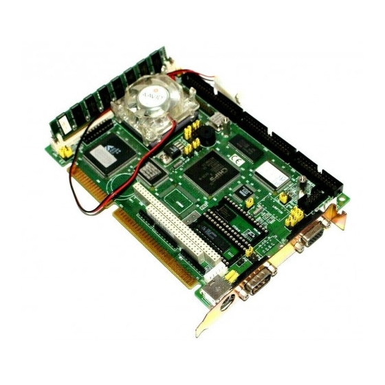
- Page 1 PCA-6145B Half-size 486 All-in-one CPU Card with Panel/CRT and Ethernet Interface PCA-6145L Half-size 486 All-in-one CPU Card with Panel/CRT Interface...
- Page 2 Copyright Notice This document is copyrighted, 2004, by Advantech Co., Ltd. All rights are reserved. Advantech Co., Ltd., reserves the right to make improve- ments to the products described in this manual at any time without notice. No part of this manual may be reproduced, copied, translated, or transmit- ted in any form or by any means without the prior written permission of Advantech Co., Ltd.
- Page 3 A Message to the Customer Advantech Customer Services Each and every Advantech product is built to the most exacting specifica- tions to ensure reliable performance in the unusual and demanding condi- tions typical of industrial environments. Whether your new Advantech...
- Page 4 Product warranty Advantech warrants to you, the original purchaser, that each of its prod- ucts will be free from defects in materials and workmanship for one year from the date of purchase. This warranty does not apply to any products which have been repaired or altered by other than repair personnel authorized by Advantech, or which have been subject to misuse, abuse, accident or improper installation.
- Page 5 Before you begin installing your card, please make sure that the following materials have been shipped: • 1 PCA-6145B/6145L CPU card • 1 6-pin mini-DIN keyboard & PS/2 mouse adapter • 1 Hard disk drive (IDE) interface cable (40 pin) •...
- Page 6 PCA-6145 User’s Manual...
-
Page 7: Table Of Contents
Figure 1.1:Dimensions(component side)......5 Figure 1.2:Jumper & Conn (component side) ....6 Figure 1.3:Jumper &Conn (solder side) ......7 Jumpers and connectors ............ 8 Table 1.1:PCA-6145B/PCA-6145L Jumpers ....8 Table 1.2:PCA-6145B/PCA-6145L Connectors..... 8 Safety precautions ............. 9 Jumper settings..............11 Chapter 2 Connecting peripherals........18... - Page 8 3.1.10 Save & Exit setup ............34 3.1.11 Exit without saving ............34 Chapter 4 Display & Ethernet Soft/Hardware Config .36 PCA-6145B/PCA-6145L Utility Disk ......36 VGA Display Software Configuration......37 Figure 4.1:VGA Setup screen........38 VGA Win 95 Driver Support .......... 39 Ethernet Software Configuration ........
- Page 9 Table C.14:Interrupt assignments ......... 68 Table C.15:Timer channel assignments......68 Appendix D Detailed system information......70 POST LEDs..............71 Table of Contents...
- Page 10 PCA-6145 User’s Manual...
- Page 11 Hardware Configuration...
-
Page 12: Chapter 1 Hardware Configuration
Chapter 1 Hardware Configuration 1.1 Introduction The PCA-6145B/6145L is a full-function CPU card which integrates the VGA LCD panel, Ethernet and other enhanced I/O interfaces on a half- size CPU card. This card uses a 80486 DX, DX2, DX4 CPU or 5x86 series and can have up to 32 MB DRAM and EDO RAM. - Page 13 • I/O bus expansion: PC/104 connector with face-up installation • SSD: Supports M-systems DiskOnChip flash disk • Flash Backup: CMOS Data Ethernet controller functions (PCA-6145B only) • Controller: UMC UM9008, built-in 8k x 16 SRAM • I/O address switchless setting •...
- Page 14 • Display BIOS: Default CRT/Toshiba TFT panel BIOS, Flash BIOS can be easily updated Mechanical and environmental • Board size: 185 mm x 122 mm • Max. power requirements: +5 V, 3.5 A • Power supply voltage: +5 V (4.75 V to 5.25 V) •...
-
Page 15: Board Layout
1.3 Board layout Figure 1.1: Dimensions(component side) - Page 16 Figure 1.2: Jumper & Conn (component side) PCA-6145 User’s Manual...
- Page 17 Figure 1.3: Jumper &Conn (solder side)
-
Page 18: Jumpers And Connectors
The table below lists the function of each of the board jumpers and con- nectors. Later sections in this chapter give instructions on setting jumpers and detailed information on each jumper setting. Chapter 2 gives instruc- tions for connecting external devices to your card. Table 1.1: PCA-6145B/PCA-6145L Jumpers Number Function Turbo LED... -
Page 19: Safety Precautions
COM2 Serial port 2 connector SBC power connector VGA connector Ethernet connector External Keyboard connector Keyboard connector Keyboard lock Speaker 1.5 Safety precautions Follow these simple precautions to protect yourself from harm and your PC from damage. Warning! 1.Please read these safety instructions carefully 2.Please keep this User‘s Manual for later reference 3.Please disconnect the board from AC outlet before cleaning. - Page 20 This device complies with the requirements in part 15 of the FCC rules: Operation is subject to the following two conditions: 1.This device may not cause harmful interference, and 2.This device must accept any interference received, including interference that may cause undesired operation This equipment has been tested and found to comply with the limits for a Class A digital device, pursuant to Part 15 of the FCC Rules.
-
Page 21: Jumper Settings
1.6 Jumper settings This section tells how to set the jumpers to configure your card. It gives the card default configuration and your options for each jumper. After you set the jumpers and install the card, you will also need to run the BIOS Setup program (discussed in Chapter 3) to configure the serial port addresses, floppy/hard disk drive types and system operating parameters. - Page 22 CPU type select In order for the system to function properly, the jumpers must be set to accommodate the CPU installed on the CPU card. CPU type select CPU Type JP4 JP5 JP6 JP7 JP8 JP11 JP13 JP14 JRN1 JRN2 JRN3 Intel DX33(5V) DX2-66...
- Page 23 CPU type select CPU Type JP4 JP5 JP6 JP7 JP8 JP11 JP13 JP14 JRN1 JRN2 JRN3 Cyrix 5x86-120 DX4-120 (3.3V)(SV8B) Intel P24D DX4-75 (5V) Cyrix DX2-66 DX2-66 (5V) TI DX2-66 (3.3V)
- Page 24 CPU type select CPU Type JP4 JP5 JP6 JP7 JP8 JP11 JP13 JP14 JRN1 JRN2 JRN3 Cyrix DX2-80 TI DX2-80 (3.3V) DX-40 DX2-80(5V) DX4-100 (NV8T) (3.3 V) Note: 1. AMD 5X86-133 JP20 ON other OFF 2. AMD DX2-80 JP21 ON other OFF Default setting: Intel DX4-100 PCA-6145 User’s Manual...
- Page 25 Watchdog timer (JP29) Watchdog timer system reset/IRQ15 select (JP29) Reset (default) IRQ15 JP29 COM2 settings for RS-232/422/485 (JP35~39) COM2 settings for RS-232/422/485 (COM2) RS-232 (default) RS-422 RS-485 JP35 JP36 JP37 JP38 JP39 Battery backup select Battery Backup (default)
- Page 26 PS/2 mouse setting PS2 Mouse (default) JP15 LCD type control LCD (default) JP28 PCA-6145 User’s Manual...
- Page 27 Connecting peripherals Chapter 2...
-
Page 28: Chapter 2 Connecting Peripherals
Chapter 2 Connecting peripherals This chapter tells how to connect peripherals, switches and indicators to the PCA-6145B/PCA-6145L board. You can access most of the connec- tors from the top of the board while it is installed in the chassis. If you have a number of cards installed, or your chassis is very tight, you may need to partially remove the card to make all the connections. -
Page 29: Enhanced Ide Connectors (Cn1)
CN2 consists of a 44-pin, dual-in-line header. Power supplies (+12V) present on CN2 depend on the supply connected to the board. The PCA-6145B/PCA-6145L provides a bias control signal on CN2 which can be used to control the LCD bias voltage. It is recommended that the LCD bias voltage (+5V) and panel video signals are stable. -
Page 30: Floppy Drive Connector (Cn3)
2.3 Floppy drive connector (CN3) You can attach up to two floppy disk drives to the PCA-6145B/PCA- 6145L's on-board controller. You can use any combination of 5.25" (360 KB and 1.2 MB) and/or 3.5" (720 KB, 1.44 MB and 2.88 MB) drives. -
Page 31: Reset Switch (Jp30)
You can connect a LED to connector JP3 to indicate when the HDD is active. Marks on the circuit board indicate LED polarity. 2.8 VGA display connector (J2) The PCA-6145B/PCA-6145L provides a VGA controller for high resolu- tion VGA interface. J2 is a DB-15 connector for VGA monitor input. 2.9 Serial Ports The PCA-6145B/PCA-6145L offers two serial ports: COM1 in RS-232, COM2 in RS-232/422/485. - Page 32 Table 2.2: Serial port connections (COM1, COM2) Connector Address COM1 RS-232 COM2 RS-232/422/485 RS-232 connection (COM1) Different devices implement the RS-232 standard in different ways. If you are having problems with a serial device, be sure to check the pin assignments for the connector.
- Page 33 RX + or receive data + (DTE) RX - or receive data - (DTE) Power connectors J1 If you prefer not to acquire power through PCA-6145B/PCA-6145L's backplane via the gold H-connectors, J1 also provide power input con- nectors for +5 V and +12 V.
- Page 34 PCA-6145 User’s Manual...
- Page 35 AWARD BIOS SETUP Chapter 3...
-
Page 36: Chapter 3 Award Bios Setup
Chapter 3 AWARD BIOS Setup 3.1 AWARD BIOS Setup Figure 3.1: Setup program initial screen Award's BIOS ROM has a built-in Setup program that allows users to modify the basic system configuration. This type of information is stored in battery-backed RAM so that it retains the Setup information when the power is turned off. -
Page 37: Standard Cmos Setup
3.1.2 Standard CMOS setup Choose the "Standard CMOS Setup" option from the Initial Setup Screen Menu, and the screen below is displayed. This standard Setup Menu allows users to configure system components such as date, time, hard disk drive, floppy drive, display, and memory. Figure 3.2: CMOS setup screen Chapter 3... -
Page 38: Bios Features Setup
3.1.3 BIOS features setup By choosing the "BIOS FEATURES Setup" option from the CMOS SETUP screen menu, the following screen is displayed. This sample scree contains the manufacturer's default values for the PCA-6145B/ PCA-6145L. Virus Warning During and after the system boots up, any attempt to write to the boot sec- tor or partition table of the hard disk drive will halt the system. - Page 39 You can run the anti-virus program to locate the problem. If Virus Warning is Disabled, no warning message will appear if anything attempts to access the boot sector or hard disk partition. CPU Internal Cache/External Cache Depending on the CPU/chipset design, these options can speed up mem- ory access when enabled.
- Page 40 Boot Up NumLock Status The default is "On". Keypad boots up to number keys. Keypad boots up to arrow keys. Boot Up System Speed High Sets the speed to high Sets the speed to low IDE HDD Block Mode Enabled Enable IDE HDD Block Mode.
- Page 41 Typematic Delay (msec) When holding down a key, the Typematic Delay is the time interval between the appearance of the first and second characters. The input val- ues (msec) for this category are: 250, 500, 750, 1000. Security Option This setting determines whether the system will boot if the password is denied, while limiting access to Setup.
-
Page 42: Chipset Features Setup
3.1.4 CHIPSET features setup By choosing the "CHIPSET FEATURES Setup" option from the CMOS Setup screen menu, the following screen is displayed. This sample screen contains the manufacturer's default values for the PCA-6145 board PCA-6145 User’s Manual... -
Page 43: Power Management Setup
3.1.5 Power management setup The power management setup controls the CPU board's "green" features. The following screen shows the manufacturer's default. Power Management This option allows you to determine if the values in power management are disabled, user-defined, or predefined. HDD Power Management You can choose to turn the HDD off after a one of the time interval listed, or when the system is in Suspend mode. -
Page 44: Load Bios Defaults
IRQ Activity IRQ can be set independently. Activity on any enabled IRQ will wake up the system. 3.1.6 Load BIOS defaults "LOAD BIOS DEFAULTS" indicates the most appropriate values for the system parameters for minimum performance. These default values are loaded automatically if the stored record created by the Setup program becomes corrupted (and therefore unusable). - Page 45 VGA Display & Ethernet Software/ Hardware Configuration...
-
Page 46: Chapter 4 Display & Ethernet Soft/Hardware Config
BIOS simply by reprogramming the Flash chip. 4.1 PCA-6145B/PCA-6145L Utility Disk The PCA-6145B/PCA-6145L is supplied with a software utility disk that holds the necessary file for setting up the VGA display and Ethernet and Win 95 controller. The disk’s directory and file structure is as follows: DIAG9008.EXE... -
Page 47: Vga Display Software Configuration
Configure the VGA display as follows: 1. Apply power to the PCA-6145B/PCA-6145L with a color TFT dis- play attached. This is the default setting for the PCA-6145B/PCA- 6145L. - Page 48 2. At the prompt, type AWDFLASH.EXE and press <Enter>. The VGA configuration program will then display the following: Figure 4.1: VGA Setup screen 3. At the prompt, type in the BIN file which supports your display. When you are sure that you have entered the file name correctly press <Enter>.
-
Page 49: Vga Win 95 Driver Support
DIAG 9008.EXE program. To execute the configuration, to view the current configuration, or to run diagnostics, do the following: 1. Power the PCA-6145B on. Ensure that the DIAG 9008.EXE file is located in the working drive. 2. At the prompt type DIAG 9008.EXE and press <Enter>. The Ethernet configuration program will then be displayed. -
Page 50: Ethernet Driver Support
4.5 Ethernet Driver Support These drivers are designed to work in a workstation environment under Windows NT, Win 95, or DOS operating system. You may install these drivers for your application. PCA-6145 User’s Manual... - Page 51 SVGA Setup Chapter 5...
-
Page 52: Chapter 5 Svga Setup
Chapter 5 SVGA Setup The 65545 VGA BIOS supports monochrome LCD, EL, color TFT and STN LCD flat panel displays. It also supports interlaced and non-inter- laced analog monitors (VGA color and VGA monochrome) in high-reso- lution modes while maintaining complete IBM VGA compatibility. Digital monitors (i.e. -
Page 53: Software Support
5.2 Software support The drivers support the following applications using the filenames and resolutions listed: Chapter 5... -
Page 54: Driver Installation
5.3 Driver installation Necessary prerequisites The instructions in this manual assume that you understand elementary concepts of MS-DOS and the IBM Personal Computer. Before you attempt to install any driver or utility you should: know how to copy files from a floppy disk to a directory on the hard disk, understand the MS- DOS directory structure, and know how to format a floppy disk. - Page 55 Changing Display Drivers in Windows To change display drivers in Windows, select the Windows Setup icon from the Main window. You will be shown the current setup configura- tion. Select Change System Settings from the Option menu. Click on the arrow at the end of the Display line.
-
Page 56: Autocad R12
Step 5: Follow the directions on the screen to complete the setup. In most cases, you may press <ENTER> to accept the suggested option. When Setup is done, it will return to DOS. Type WIN <ENTER> to start Windows with the new display driver. Changing Display Drivers in DOS To change display drivers from DOS, change to the Windows directory and run Setup, repeating steps 4 and 5 from the previous page. - Page 57 olutions. Using the arrow keys and the <ENTER> key, select the resolutions that are appropriate for your monitor. When all of the desired resolutions have been selected, press <END> to begin the installation. At this point you will be asked for a drive and directory to copy the driver files.
-
Page 58: Lotus 1-2-3 And Lotus Symphony
This menu allows you to modify: Display List Enable/Disable Drawing CacheEnable/Disable Use Acad 31 bit space?Yes/No Internal Command EchoEnable/Disable BP Zoom ModeFreeze/Float Regen Mode Incremental/Fast If your previously installed driver is not TurboDLD, you will have to reconfigure the RENDER command the first time you use it. 5.3.3 Lotus 1-2-3 and Lotus Symphony These drivers are designed to work with Lotus 1-2-3 versions 2.0, 2.01 and 2.2, and with Lotus Symphony versions 1.0 and 1.1. -
Page 59: Vesa
INSTALL <ENTER> Step 3: The Lotus installation program will load and present the instal- lation menu. From this menu, select Advanced Options. From the Advanced Options menu, select Add New Drivers To Library. From the Add New Drivers Menu, select Modify Cur- rent Driver Set. -
Page 60: Word
Driver installation Step 1: Place the display driver diskette into drive A. Make A the default drive by typing A: <ENTER>. Run the SETUP program by typing SETUP <ENTER>. Press any key to display a list of supported applications. Use the arrow keys to select VESA Driver Version 1.2 and press <ENTER>. -
Page 61: Wordperfect
tion process. A default drive and directory path will be dis- played. Use the backspace key to erase this and type in your Word directory. After the files have been installed, press any key to return to the list of supported applications. Press <ESC> followed by Y to exit to DOS. - Page 62 Configuring WordPerfect 5.0 for 132 columns Follow these instructions to configure WordPerfect 5.0 for 132 column text mode: Step 1: To use the SETCOL program to set 132 columns and 25 rows, type the following command: SETCOL 132, 25 <ENTER> Step 2: Start WordPerfect.
- Page 63 Programming the Watchdog Timer...
-
Page 64: Appendix A Programming The Watchdog Timer
Appendix A Programming the Watchdog Timer A.1 Programming the watchdog timer If you decide to program the watchdog timer, you must write a program which reads I/O port address 443 (hex). The output data is a timer value. You can write it from 01 (hex) to 3F (hex), and the related timer is 1 sec. to 63 sec. - Page 65 Upgrading Appendix B...
-
Page 66: Appendix B Upgrading
Appendix B Upgrading B.1 Installing PC/104 modules (CN5,CN6) The PCA-6145B/PCA-6145L card's PC/104 connector lets you attach PC/104 modules. These modules perform the functions of traditional plug-in expansion cards, but save space and valuable slots. Advantech modules include: • PCM-3110 PCMCIA module •... - Page 67 Figure B.1: PC/104 module dimensions (mm)(+/-0.1) Appendix B...
-
Page 68: Installing Dram (Simms)
B.2.1 Memory sizes The board accepts 1 MB, 2 MB, 4 MB, 8 MB, 16 MB, 32 MB and EDO RAM. The following table lists some of the different memory configura- tions for the PCA-6145B/PCA-6145L card. SIMM 1Total 1 MB 1 MB... - Page 69 Detailed system information This appendix contains information of a detailed or specialized nature. It includes: • Parallel connector pin assignments • HDD connector pin assignments • FDD connector pin assignments • Keyboard connector pin assignments • CRT display connector • Flat panel display connector •...
-
Page 70: Appendix C Detailed System Information
Appendix C Detailed system information Table C.1: Parallel/printer connector (CN4) Pin no. Signal STROBE DATA 0 DATA 1 DATA 2 DATA 3 DATA 4 DATA 5 DATA 6 DATA 7 - ACKNOWLEDGE BUSY PAPER EMPTY + SELECT - AUTO FEED - ERROR - INIT PRINTER - SELECT INPUT... - Page 71 Pin no. Signal Pin no. Signal N.C. -ACT Table C.3: FDD connector (CN3) Pin no. Signal 1-33 (odd) GROUND HIGH DENSITY 4, 6 UNUSED INDEX MOTOR ENABLE A DRIVER SELECT B DRIVER SELECT A MOTOR ENABLE B DIRECTION STEP PULSE WRITE DATA WRITE ENABLE TRACK 0...
-
Page 72: Vga Display Connector (J2)
C.0.1 VGA display connector (J2) Table C.5: PCA-6145 CRT display connector Signal Pin Signal GREEN 10 BLUE H-SYNC V-SYNC C.0.2 Flat panel display connector (CN2) mini pin header Table C.6: PCA-6145 Flat panel display connector Function Function +12 V +12 V ENAVEE8 SHFCLK36 ENABKL... -
Page 73: Rs-232 Connections (Com1, Com2)
C.0.3 RS-232 connections (COM1, COM2) Different devices implement the RS-232 standard in different ways. If you are having problems with a serial device, be sure to check the pin assignments for the connector. The following table shows the pin assign- ments for the card's RS-232 port: Table C.7: RS-232 connector pin assignment Signal... - Page 74 Table C.8: PC/104 Connector Pin Assignments IOCHCHK*0V SBHE* MEMCS16* RESETDRVLA23 IOCS16* LA22 IRQ10 IRQ9 LA21 IRQ11 LA20 IRQ12 DRQ2 LA19 IRQ15 -12V LA18 IRQ14 OWS* LA17* DACK0* MEMR* DRQ0* IOCHRDYNC MEMW* DACK5* SMEMW*SD8 DRQ5 SA19 SMEMR*SD9 DACK6* SA18 IOW* SD10 DRQ6 SA17 IOR*...
- Page 75 Table C.9: System I/O ports Addr. range (Hex) Device 000-01F DMA controller 020-021 Interrupt controller 1, master 022-023 Chipset address 040-05F 8254 timer Watchdog timer disable 060-06F 8042 (keyboard Controller) 070-07F Real-time clock, non-maskable interrupt (NMI) mask 080-09F DMA page register, 0A0-0BF Interrupt controller 2 0C0-0DF...
- Page 76 Table C.10: System information I/O addresses Address Description 00-0D * Real-time clock information Second Second alarm Minutes Minute alarm Hours Hours alarm Day of week Date of month Month Year Status register A Status register B Status register C Status register D * Diagnostic status byte * Shutdown status byte Diskette drive type byte, drives A and B...
- Page 77 Table C.11: DMA channel assignments Channel Function Spare (8-bit transfer) SDLC (8-bit transfer) Floppy disk (8-bit transfer) Spare (8-bit transfer) Cascade for DMA controller 1 Spare (16-bit transfer) Spare (16-bit transfer) Spare (16-bit transfer) Table C.12: DMA controller registers Address Command code CH0 base and current address CH0 base and current word count...
- Page 78 Table C.14: Interrupt assignments Priority Interrupt# Interrupt source Parity error detected IRQ 0 Interval timer, counter 0 output IRQ 1 Keyboard IRQ 2 Interrupt from controller 2 (cascade) IRQ 8 Real-time clock IRQ 9 Cascaded to INT 0AH (IRQ 2) IRQ 10 Reserved IRQ 11 Reserved IRQ 12 PS/2 mouse...
- Page 79 POST LEDs Appendix D...
- Page 80 You can also determine the number of the test that failed by reading the LED indicators on the top of the PCA-6145B/PCA-6145L board. Please make a note of any POST error codes before you contact Advan- tech for technical support.
- Page 81 I/O address 80H. If the test fails, the code will stay in memory. You can read the code and determine which test has failed. The PCA-6145B/PCA-6145L’s POST LED indicators make this process extremely easy. You don’t need any special diagnostic tools, you just read the POST code from the LEDs.
- Page 82 Code Name Description of check-point Processor test 1 Processor status (IFLAGS) verifica- tion tests the following processor status flags, carry, zero, sign, BIOS overflow. It will set each of these flags, verify that they are set, then turn each flag off and verify it is off. Processor test 2 Read, write, verify all CPU registers except SS, SP, and BP with data...
- Page 83 Code Name Description of check-point Initialize keyboard detect type of keyboard controller (optional). Set num_lock status. Initialize video interface Detect CPU clock. Read interface CMOS location 14h to find out type of video in use. Detect and initialize video adaptor. Test video memory Test video memory, write sign-on message to screen.
- Page 84 Code Name Description of check-point Test EISA extended If EISA mode flag is set then test memory EISA memory found in slot initialization. Note: this will be skipped in ISA mode and can be ‘skipped” with ESC key in EISA mode.
- Page 85 Code Name Description of check-point Set numlock Set numlock status according to setup. Boot attempt Set low stack boot via INT 19h. Spurious If interrupt occurs in protected mode. Unclaimed NMI If unmasked NMI occurs, display "Press F1 to disable NMI, F2 to reboot".
- Page 86 PCA-6145 User’s Manual...
Need help?
Do you have a question about the PCA-6145B and is the answer not in the manual?
Questions and answers