
Related Manuals for Advantech PCM-9363


Summary of Contents for Advantech PCM-9363
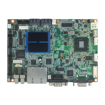
- Page 1 User Manual PCM-9363 ® 3.5" Biscuit with Intel Atom™ N455/D525, DDR3, 24-bit LVDS, CRT or HDMI, 2 Giga LAN, Mini PCIe, 3 COM...
- Page 2 Creative is a trademark of Creative Technology LTD. CHRONTEL is a trademark of Chrontel Inc. All other product names or trademarks are properties of their respective owners. Part No. 2006936310 Edition 1 Printed in China December 2010 PCM-9363 User Manual...
- Page 3 Product name and serial number – Description of your peripheral attachments – Description of your software (operating system, version, application software, etc.) – A complete description of the problem – The exact wording of any error messages PCM-9363 User Manual...
-
Page 4: Ordering Information
Packing List Before installation, please ensure the following items have been shipped: Item Part Number 1 PCM-9363 SBC 1 Startup manual 1 Utility CD 1 mini jumper pack Cables Part Number Description 1700008941 SATA cable 7P w/ Lock 32cm 1703060191 Keyboard/mouse cable 1*6P-2.0/M-DIN 6P(F)*2 19 cm... - Page 5 Caution! There is a danger of a new battery exploding if it is incorrectly installed. Do not attempt to recharge, force open, or heat the battery. Replace the battery only with the same or equivalent type recommended by the man- ufacturer. Discard used batteries according to the manufacturer's instructions. PCM-9363 User Manual...
- Page 6 PCM-9363 User Manual...
-
Page 7: Table Of Contents
Figure 2.3 Board dimension layout (component side) ....16 Figure 2.4 Board dimension layout (solder side) ....... 16 Figure 2.5 Board dimension layout (coastline) ......17 Figure 2.6 PCM-9363 HDMI mechanical drawing (top View) ..17 Chapter BIOS settings ........19 Introduction ..................... - Page 8 Table A.14:CN16: 18 or 24 bits LVDS Panel......62 Table A.15:CN17: Single LAN (Optional) ........63 Table A.16:CN18: LAN1 ............. 64 Table A.17:CN19: LAN2 ............. 64 Table A.18:CN20: Power Switch (Low Active)......64 Table A.19:CN21: LPT..............65 PCM-9363 User Manual viii...
- Page 9 Table C.1: System I/O Ports ............86 1st MB Memory Map ................86 Table C.2: 1st MB memory map ..........86 DMA Channel Assignments ..............87 Table C.3: DMA channel assignments........87 Interrupt Assignments ................87 Table C.4: Interrupt assignments ..........87 PCM-9363 User Manual...
- Page 10 PCM-9363 User Manual...
-
Page 11: Chapter 1 General Introduction
Chapter General Introduction This chapter gives background information on the PCM-9363. Sections include: ! Introduction ! Product feature ! Specifications... -
Page 12: Introduction
Introduction PCM-9363 is a 3.5" SBC (Single Board Computer) with Embedded Intel® Atom™ N455 1.66 GHz/D525 1.8 GHz Processor. The PCM-9363 can support DDR3 mem- ory up to 4 GB for D525, has six USB 2.0 compatible ports, two Giga-LAN (1000Mbps) interface, LVDS and VGA support, with HDMI (optional), HD (High Defi- nition) audio, and one Mini-PCIe expansion slot. -
Page 13: Specifications
6 USB 2.0 ports which are high-speed, full- speed, and low- USB Interface speed capable USB Connector:(USB1~4) 2 set 5 x 2-pin Hirose DF13 type Full ACPI (Advanced Configuration and Power Interface) 2.0 Power Management Supports S0, S1, S3,S4, S5 BIOS AMI 16Mb Flash BIOS via SPI PCM-9363 User Manual... -
Page 14: Mechanical Specifications
20 mm (heatsink without fan for N455 SKU) 1.3.2.3 Height under bottom (mm) 9.00 mm (CF Socket) 1.3.2.4 Weight (g) with Heatsink 110 g (heatsink with fan for D525 SKU) 88 g (heatsink without fan for N455 SKU) PCM-9363 User Manual... -
Page 15: Electrical Specifications
Operating Temperature Operating temperature: 0 ~ 60° C (32~140°F) 1.4.3 Storage Humidity Standard products (0 ~ 60° C) Relative humidity: 95% @ 60° C 1.4.4 Storage Temperature Standard products (0 ~ 60° C) Storage temperature: -20~70° C PCM-9363 User Manual... - Page 16 PCM-9363 User Manual...
-
Page 17: Chapter 2 H/W Installation
Chapter H/W Installation This chapter explains the setup procedures of the PCM-9363 hard- ware, including instructions on setting jumpers and connecting peripherals, as well as switches, indicators and mechanical draw- ings. Be sure to read all safety precautions before you begin the... -
Page 18: Jumpers
When clearing CMOS, before turning on the power supply, set the jumper back to 3.0 V Battery On. 2.1.2 Jumper list Table 2.1: Jumper List COM2 Setting AT / ATX Power SEL Clear CMOS Panel Voltage SEL PCM-9363 User Manual... -
Page 19: Jumper Settings
Function (1-2) (default) AT Power SEL EMPTY ATX Power Table 2.4: J4: Clear CMOS Part Number 1653003101 Footprint HD_3x1P_79_D Description PIN HEADER 3*1P 180D(M) 2.0mm DIP SQUARE W/O Pb Setting Function (1-2) (default) Normal (2-3) Clear CMOS PCM-9363 User Manual... -
Page 20: Table 2.5: J5: Pan Vol Sel
Table 2.5: J5: PAN VOL SEL Part Number 1653003101 Footprint HD_3x1P_79_D Description PIN HEADER 3*1P 180D(M) 2.0mm DIP SQUARE W/O Pb Setting Function (1-2) (2-3) (default) PCM-9363 User Manual... -
Page 21: Connectors
Power Switch (Low Active) CN21 CN22 HDMI (Optional) CN23 Reset CN24 External USB CN25 External USB CN26 COM1 CN27 CN28 Mini PCIE lock CN29 Mini PCIE slot CN30 DDR3 SODIMM CN31 BIOS Socket CN32 CN36 SATA Power PCM-9363 User Manual... -
Page 22: Connector Settings
2.2.2.2 SATA Connector (CN2, CN3) PCM-9363 supports Serial ATA via two connectors (CN2, CN3). Data transfer rates up to 300 MB/s are possible, enabling very fast data and file transfer, and indepen- dent DMA operation on two ports. 2.2.2.3 GPIO (General Purpose Input Output) (CN4) The board supports 8-bit GPIO through GPIO connector. - Page 23 2.2.2.10 Inverter Power Connector (CN13) PCM-9363 can provide +5 V and +12 V and signal to LCD inverter board via CN13. 2.2.2.11 USB Connectors (CN14, CN15, CN24, CN25) The board provides up to six USB (Universal Serial Bus) ports.
- Page 24 2.2.2.15 LPT Connector (CN21) PCM-9363 can support LPT via CN21. LPT (Line Print Terminal) is the original, yet still common, name of the parallel port interface on IBM PC-compatible computers. It was designed to operate a text printer that used IBM's 8-bit extended ASCII charac- ter set.
-
Page 25: Mechanical
Mechanical 2.3.1 Jumper and Connector Locations Figure 2.1 Jumper and Connector layout (component side) Figure 2.2 Jumper and connector layout (solder side) PCM-9363 User Manual... -
Page 26: Board Dimensions
2.3.2 Board Dimensions Figure 2.3 Board dimension layout (component side) Figure 2.4 Board dimension layout (solder side) PCM-9363 User Manual... -
Page 27: Figure 2.5 Board Dimension Layout (Coastline)
Figure 2.5 Board dimension layout (coastline) Figure 2.6 PCM-9363 HDMI mechanical drawing (top View) PCM-9363 User Manual... - Page 28 PCM-9363 User Manual...
-
Page 29: Chapter 3 Bios Settings
Chapter BIOS settings... -
Page 30: Introduction
AMIBIOS has been integrated into a slew of motherboards for over two decades. With the AMIBIOS Setup program, you can modify BIOS settings and control the var- ious system features. This chapter describes the basic navigation of the PCM-9363 BIOS setup screens. -
Page 31: Main Setup
Date using the <Arrow> keys. Enter new values through the keyboard. Press the <Tab> key or the <Arrow> keys to move between fields. The date must be entered in MM/DD/YY format. The time must be entered in HH:MM:SS format. PCM-9363 User Manual... -
Page 32: Advanced Bios Features Setup
3.2.2 Advanced BIOS Features Setup Select the Advanced tab from the PCM-9363 setup screen to enter the Advanced BIOS Setup screen. You can select any of the items in the left frame of the screen, such as CPU Configuration, to go to the sub menu for that item. You can display an Advanced BIOS Setup option by highlighting it using the <Arrow>... -
Page 33: Figure 3.4 Cpu Configuration Setting
CPU speed is controlled by the operating system. Intel® C-STATE tech This item allows the CPU to save more power under idle mode. Enhanced C-States CPU idle set to enhanced C-States, disabled by Intel® C-STATE tech item. PCM-9363 User Manual... -
Page 34: Figure 3.5 Ide Configuration
Hard Disk Write Protect Disable/Enable device write protection. This will be effective only if the device is accessed through BIOS. IDE Detect Time Out (Sec) This item allows you to select the time out value for detecting ATA/ATAPI device(s). PCM-9363 User Manual... -
Page 35: Figure 3.6 Super I/O Configuration
This item allows you to select parallel port mode. Parallel Port IRQ This item allows you to select parallel port IRQ. Auto Flow Control For SP2 This item allows you to enable or disable auto flow control. PCM-9363 User Manual... -
Page 36: Figure 3.7 Hardware Health Configuration
Figure 3.7 Hardware health configuration H/W Health Function This item allows you to control H/W monitoring. Temperature & Voltage show CPU/System Temperature Vcore / +3.3 Vin / +5 Vin / +12 Vin / VBAT Fan1 Speed show Display Fan1 Speed RPM. PCM-9363 User Manual... -
Page 37: Figure 3.8 Acpi Settings
General ACPI Configuration Figure 3.9 General ACPI Configuration – Suspend mode Select the ACPI state used for system suspend. – Report Video on S3 Resume This item allows you to invoke VA BIOS POST on S3/STR resume. PCM-9363 User Manual... -
Page 38: Figure 3.10Advanced Acpi Configuration
Include APIC table pointer to RSDT pointer list. – AMI OEMB table Include OEMB table pointer to R(x)SDT pointer lists. – Headless mode Enable / Disable Headless operation mode through ACPI. Chipset ACPI Configuration Figure 3.11 Chipset ACPI Configuration PCM-9363 User Manual... -
Page 39: Figure 3.12Ahci Configuration
Enable/Disable High performance Event timer. 3.2.2.6 AHCI Configuration Figure 3.12 AHCI Configuration AHCI Port0 / Port1 While entering setup, BIOS auto detects the presence of IDE devices. This dis- plays the status of auto detection of IDE device. PCM-9363 User Manual... -
Page 40: Figure 3.13Apm Configuration
Hard Disk Power Down Mode Power down Hard Disk in suspend or standby mode. Resume On Ring Enable / Disable RI to generate a wake event. Resume On RTC Alarm Enable / Disable RTC to generate a wake event. PCM-9363 User Manual... -
Page 41: Figure 3.14Event Log Configuration
Mark all events as read Mark all unread events as read. Clear Event Log Discard all events in the event Log. 3.2.2.9 MPS Configuration Figure 3.15 MPS Configuration MPS Revision This item allows you to select MPS (Multi-Processor Specification) version. PCM-9363 User Manual... -
Page 42: Figure 3.16Smbios Configuration
Figure 3.17 USB Configuration Legacy USB Support Enables support for legacy USB. Auto option disables legacy support if no USB devices are connected. USB 2.0 Controller Mode This item allows you to select HiSpeed(480Mbps) or FullSpeed (12Mpbs). PCM-9363 User Manual... -
Page 43: Figure 3.18Usb Mass Storage Device Configuration
If Auto, any USB device less than 530MB will be emulated as a floppy drive and the remaining as hard drives. Force FDD option can be used to force a FDD formatted drive to boot as FDD (Ex. ZIP drive). PCM-9363 User Manual... -
Page 44: Advanced Pci/Pnp Settings
3.2.3 Advanced PCI/PnP Settings Select the PCI/PnP tab from the PCM-9363 setup screen to enter the Plug and Play BIOS Setup screen. You can display a Plug and Play BIOS Setup option by highlight- ing it using the <Arrow> keys. All Plug and Play BIOS Setup options are described in this section. -
Page 45: Boot Settings
ISA devices. 3.2.3.10 Reserved Memory Size This item allows you to reserve the size of memory block for legacy ISA device. 3.2.4 Boot Settings Figure 3.20 Boot Setup Utility 3.2.4.1 Boot Settings Configuration Figure 3.21 Boot Setting Configuration PCM-9363 User Manual... -
Page 46: Security Setup
Security Setup Figure 3.22 Password Configuration Select Security Setup from the PCM-9363 Setup main BIOS setup menu. All Security Setup options, such as password protection and virus protection are described in this section. To access the sub menu for the following items, select the item and press <Enter>:... -
Page 47: Advanced Chipset Settings
North Bridge Chipset Configuration Figure 3.24 North Bridge Configuration DRAM Frequency This item allows you to manually change DRAM frequency. Configure DRAM Timing by SPD This item allows you to enables or disable detection by DRAM SPD. PCM-9363 User Manual... -
Page 48: Figure 3.25Video Function Configuration
This item allows you to enable or disable the spread spectrum clock. – Backlight Control1/2 Type This item allows you to select backlight control type. – Backlight 1/2 Level This item allows you to select backlight level. PCM-9363 User Manual... -
Page 49: Figure 3.26South Bridge Configuration
SLP_S4# is a signal for power plane control. This signal shuts off power to all non-critical systems when in the S4 (Suspend to disk) or S5 (Soft off) state. This setting indicates minimum assertion width of the SLP_S4# signal to ensure that the DRAMs have been safely power-cycled. PCM-9363 User Manual... -
Page 50: Exit Option
3.2.7.3 Load Optimal Defaults The PCM-9363 automatically configures all setup items to optimal settings when you select this option. Optimal defaults are designed for maximum system performance, but may not work best for all computer applications. In particular, do not use the Opti- mal Defaults if your computer is experiencing system configuration problems. - Page 51 Select Load Fail-Safe Defaults from the Exit menu and press <Enter>. The following message appears: Load Fail-Safe Defaults? [OK] [Cancel] Select OK to load Fail-Safe defaults. PCM-9363 User Manual...
- Page 52 PCM-9363 User Manual...
-
Page 53: Chapter 4 S/W Introduction & Installation
Chapter S/W Introduction & Installation... -
Page 54: S/W Introduction
SUSI is such an abstraction layer. SUSI provides a uniform API for application programmers to access the hardware functions in different Operating Systems and on different hardware platforms. PCM-9363 User Manual... -
Page 55: Software Apis
The Brightness Control API allows a developer to interface with an embed- ded device to easily control brightness. Backlight Control – The Backlight API allows a developer to control the backlight (screen) on/off in an embedded device. PCM-9363 User Manual... -
Page 56: Susi Utilities
The eSOS is a small OS stored in BIOS ROM. It will boot up in case of a main OS crash. It will diagnose the hardware status, and then send an e-mail to a designated administrator. The eSOS also provides remote connection: Telnet server and FTP server, allowing the administrator to rescue the system. PCM-9363 User Manual... -
Page 57: Susi Installation
If a previous version is located, please see the [Maintenance Setup] section. If it is not located, an alternative window appears. Click Next. PCM-9363 User Manual... -
Page 58: Susi Sample Programs
Visual C++ 6.0 on Windows XP or under Microsoft Embedded Visual C++ 4.0 on Windows CE. Developers must add the header file Susi.h and library Susi.lib to their own projects when they want to develop something with SUSI. PCM-9363 User Manual... - Page 59 The GPIO pin assignments of the supported platforms are located in Appendix B. Test Read Single Input Pin – Click the radio button- Single-Pin. – Key in the pin number to read the value of the input pin. The Pin number starts from '0'. PCM-9363 User Manual...
- Page 60 Key in the slave device address in Slave address field. – Key in the register offset in Register Offset field. – Click the READ A BYTE button and then a byte of data from the device will be shown on the Result field. PCM-9363 User Manual...
- Page 61 Key in the slave device address in the Slave address field. – Key in the register offset in the Register Offset field. – Click the READ SMBus DATA button and then a word of data from the device will be shown on the Result field. PCM-9363 User Manual...
- Page 62 The application can turn on or turn off the screen shot freely, and it also can tune the brightness of the panels if your platform is being supported. You can test the function- alities of VGA control as follows: PCM-9363 User Manual...
- Page 63 Before the timer counts down to zero, you can reset the timer by clicking the REFRESH button. After you click this button, the Timeout Countdown field will display the value of the SET TIMEOUT field. If you want to stop the watchdog timer, just click the STOP button. PCM-9363 User Manual...
- Page 64 If certain data values are not supported by the platform, the correspondent data field will be grayed-out with a value of 0. For more details on PCM-9363 software API, please contact your dealer PCM-9363 User Manual...
-
Page 65: Appendix Apin Assignments
Appendix PIN Assignments... -
Page 66: Pin Assignments
BOX HEADER SMD 5*2 180D (M) 2.0mm Pin Name LOUTR LINR LOUTL LINL MIC1R MIC1L Matching Cable: 1703100152 Table A.2: CN2: SATA Part Number 1654002320 Footprint FOX_LD1107V-S33T5 Description Serial ATA 7P 1.27 90D(M) SMD LD1107V-S33T5 Pin Name PCM-9363 User Manual... -
Page 67: Table A.3: Cn3: Sata
FOX_LD1107V-S33T5 Description Serial ATA 7P 1.27 90D(M) SMD LD1107V-S33T5 Pin Name Table A.4: CN4: GPIO Part Number 1653005261 Footprint HD_5x2P_79 Description PIN HEADER SMD 5*2P 180D(M) 2.0mm Pin Name GPIO4 GPIO0 GPIO5 GPIO1 GPIO6 GPIO2 GPIO7 GPIO3 PCM-9363 User Manual... -
Page 68: Table A.5: Cn5: Hdd & Pwr Led
WAFER BOX 2.0mm 6P 180D(M) W/LOCK Pin Name Power LED+ Power LED- HDD LED+ HDD LED- Table A.6: CN6: 12 V Power Input Part Number 1655404090 Footprint ATXCON-2X2-42 Description ATX PWR CONN. 2*2P 180D 4.2mm 24W4310-04S10-01T Pin Name +12V +12V PCM-9363 User Manual... -
Page 69: Table A.7: Cn8: Com3
BOX HEADER SMD 5*2P 180D(M) 2.0mm Pin Name DCD# DSR# RTS# CTS# DTR# Matching Cable: TBD Table A.8: CN10: PS2 Part Number 1655306020 Footprint WHL6V-2M Description WAFER BOX 2.0mm 6P 180D(M) W/LOCK Pin Name KBCLK KBDAT MSCLK MSDAT Matching Cable: 1703060053 1700060202 PCM-9363 User Manual... -
Page 70: Table A.9: Cn11: Smbus
Description BOX HEADER SMD 7*2P 180D(M) 2.0mm Pin Name DCD# DSR# RTS# CTS# DTR# 422TX+/485+ 422TX-/485- 422RX+ 422RX- Note: Pins 1 ~ 10: RS-232; Pins 11 ~ 12: RS-485; Pins 11 ~ 14: RS-422 Matching Cable: 1701140201 PCM-9363 User Manual... -
Page 71: Table A.11:Cn13: Inverter Power Output
WAFER BOX 2.0mm 5P 180D(M) DIP WO/pb JIH VEI Pin Name +12V ENABKL Table A.12: CN14: Internal USB Part Number 1653005260 Footprint HD_5x2P_79_N10 Description PIN HEADER 2*5P 180D(M) 2.0mm SMD IDIOT-PROOF Pin Name A_D- B_D- A_D+ B_D+ Matching Cable: 1703100121 PCM-9363 User Manual... -
Page 72: Table A.13:Cn15: Internal Usb
B_D- A_D+ B_D+ Matching Cable: 1703100121 Table A.14: CN16: 18 or 24 bits LVDS Panel Part Number 1653910261 Footprint SPH10X2 Description *CONN. SMD 10*2P 180D(M)DF13-20DP-1.25V(91) HRS Pin Name LVDS0_D0+ LVDS0_D0- LVDS0_D1+ LVDS0_D1- LVDS0_D2+ LVDS0_D2- LVDS0_CLK+ LVDS0_z_D3+ LVDS0_CLK- PCM-9363 User Manual... -
Page 73: Table A.15:Cn17: Single Lan (Optional)
Table A.14: CN16: 18 or 24 bits LVDS Panel LVDS0_z_D3- +5V or +3.3V +5V or +3.3V Table A.15: CN17: Single LAN (Optional) Part Number 1652002996 Footprint RJ45_14P_RTA-195AAK1A Description PHONE JACK RJ45 14P 90D(M) DIP RTA-195AAK1A Pin Name TX+(10/100),BI_DA+(GHz) TX-(10/100),BI_DA-(GHz) RX+(10/100),BI_DB+(GHz) BI_DC+(GHz) BI_DC-(GHz) RX-(10/100),BI_DB-(GHz) BI_DD+(GHz) BI_DD-(GHz) PCM-9363 User Manual... -
Page 74: Table A.16:Cn18: Lan1
Part Number 1652002996 Footprint RJ45_14P_RTA-195AAK1A Description Phone Jack RJ45 14P 90D(M) DIP RTA-195AAK1A Pin Name Table A.18: CN20: Power Switch (Low Active) Part Number 1655302020 Footprint WF_2P_79_BOX_R1_D Description WAFER BOX 2P 180D(M) 2.0mm W/Lock Pin Name PSIN PCM-9363 User Manual... -
Page 75: Table A.19:Cn21: Lpt
Table A.19: CN21: LPT Part Number 1653213260 Footprint HD_13x2P_79_BOX Description BOX HEADER 13*2P 180D(M) 2.0mm SMD Pin Name STROBE# AUTOFEED# ERROR# INIT# SLCT IN# ACK# BUSY SLCT Matching Cable: 1700260250 1700001531 PCM-9363 User Manual... -
Page 76: Table A.20:Cn22: Hdmi (Optional)
Table A.20: CN22: HDMI (Optional) CN22 HDMI Part Number 1654009225 Footprint HDMI_19P_QJ51193-FFD4-4F Description HDMI Conn 19P 0.5mm 90D(M) SMD QJ51193-FFB4-7F Pin Name HDMI_D2+ HDMI_D2- HDMI_D1+ HDMI_D1- HDMI_D0+ HDMI_D0- HDMI_CLK+ HDMI_CLK- HDMI_z_CEC HDMI_SCL HDMI_SDA +V5_HDMI HDMI_z_DET PCM-9363 User Manual... -
Page 77: Table A.21:Cn23: Reset
Table A.21: CN23: Reset Part Number 1655302020 Footprint WF_2P_79_BOX_R1_D Description WAFER BOX 2P 180D(M) 2.0mm W/Lock Pin Name RESET# Table A.22: CN24: External USB Part Number 1654904105 Footprint USB-V-4A Description USB CON. 4P 90D(F) DIP A TYPE RoHS Pin Name PCM-9363 User Manual... -
Page 78: Table A.23:Cn25: External Usb
1654904105 Footprint USB-V-4A Description USB CON. 4P 90D(F) DIP A TYPE RoHS Pin Name Table A.24: CN26: COM1 Part Number 1654000056 Footprint DBCOM-VM5MS Description D-SUB CON. 9P 90D(M)DIP 070241MR009S200ZU SUYIN Pin Name DCD# DTR# DSR# RTS# CTS# PCM-9363 User Manual... -
Page 79: Table A.25:Cn27: Vga
Table A.25: CN27: VGA Part Number 1654000055 Footprint DBVGA-VF5MS Description D-SUB Conn. 15P 90D(F) DIP 070242FR015S200ZU Pin Name GREEN BLUE DDAT HSYNC VSYNC DCLK PCM-9363 User Manual... -
Page 80: Table A.26:Cn28: Mini Pcie Lock
MINI PCI Express LATCH 52P 90D SMD 6.8mm Pin Name Table A.27: CN29: Mini PCIE slot Part Number 1654002538 Footprint FOX_AS0B226-S68K7F Description MINI PCI express 52P 90D SMD H=6.8mm Pin Name WAKE# +3.3V or +3.3VSB +1.5V CLKREQ# REFCLK- REFCLK+ PCM-9363 User Manual... - Page 81 Table A.27: CN29: Mini PCIE slot PERST# PERn0 +3.3VSB PERp0 +1.5V SMB CLK PETn0 SMB DAT PETp0 USB D- USB D+ +3.3V or +3.3VSB +3.3V or +3.3VSB +1.5V +3.3V or +3.3VSB PCM-9363 User Manual...
-
Page 82: Table A.28:Cn30: Ddr3 Sodimm
Table A.28: CN30: DDR3 SODIMM Part Number 1651001904 Footprint DDR-SODIMM-STD65 Description SKT DIMM 200P DDR2 H=6.5mm STD SMD WO/Pb Pin Name VREF DQ59 DQ63 DQ58 DQ62 DQS#7 DQS7 DQ57 DQ56 DQ61 DQ60 DQ51 DQ50 DQ55 PCM-9363 User Manual... -
Page 83: Table A.29:Cn31: Bios Socket
Table A.28: CN30: DDR3 SODIMM DQ54 Table A.29: CN31: BIOS Socket Part Number 1651000682 Footprint SOCKET_8P_ACA-SPI-004-K01 Description IC SKT 8P SMD WO/Pb C ACA-SPI-004-K01 Pin Name HOLD# +3.3V PCM-9363 User Manual... -
Page 84: Table A.30:Cn32: Cf
Table A.30: CN32: CF Part Number 1653002919 Footprint CF_50P_CFCMD-35T15W100 Description CF Type2 Conn.50P 90D(M) SMD WO/Pb CFCMD-35T15W1 Pin Name CS0# CD2# CD1# PCM-9363 User Manual... -
Page 85: Table A.31:Cn36: Sata Power
Table A.31: CN36: SATA Power CN36 SATA Power Part Number 1655000453 Footprint WF_4P_98_BOX_R1_D Description WAFER BOX 2.0mm 5P 180D(M) DIP WO/Pb JIH VEI Pin Name +12V PCM-9363 User Manual... - Page 86 PCM-9363 User Manual...
-
Page 87: Wdt & Gpio
Appendix WDT & GPIO... -
Page 88: Watchdog Timer Sample Code
;Minutes=0 (default) Seconds=1 ;==================================================== mov dx,SCH3114_IO + 65h ; mov al,080h out dx,al ;==================================================== ;66H ;WDT timer time-out value ;bit[7:0]=0~255 ;==================================================== mov dx,SCH3114_IO + 66h mov al,01h out dx,al ;==================================================== ;bit[0] status bit R/W ;WD timeout occurred =1 PCM-9363 User Manual... -
Page 89: Gpio Sample Code
; n means which group of GPIO you want to set bl= the n group of gpio config bit 0 = gpio 0 , 0 => output pin; 1 => input pin bit 1 = gpio 1 , 0 => output pin; 1 => input pin ..PCM-9363 User Manual... - Page 90 1 = gpio 1 , 0 => Low; 1 => High ..bit 7 = gpio 7 , 0 => Low; 1 => High ; output: ax=5E78 ;function success, other value means function fail ;=========================================================== ax,5e87h bh,00h ax,5e78h next_test dx, Error_Str1 ah,09h Finish_Test next_test: PCM-9363 User Manual...
- Page 91 ;4. Set GPIO 0,2,4,6 Output differential ;restore NO. of GPIO chip push ;save NO. of GPIO chip ax,5e87h bx,0411h ;5. Check GPI 1,3,5,7 value ;restore NO. of GPIO chip push ;save NO. of GPIO chip ax,5e87h bx,03FFh ;restore NO. of GPIO chip PCM-9363 User Manual...
- Page 92 ;restore NO. of GPIO chip push ;save NO. of GPIO chip ax,5e87h bx,0300h ;restore NO. of GPIO chip push ;save NO. of GPIO chip al,Fail_lenght dx, Fail_Str dx,ax bl,0ffh test_result ;4. Set GPIO 1,3,5,7 Output differential ;restore NO. of GPIO chip PCM-9363 User Manual...
- Page 93 ;restore NO. of GPIO chip push ;save NO. of GPIO chip al,Success_lenght dx, Success1_Str dx,ax ;Do Second PCA9554 test ;1.Set GPIO 0,2,4,6 as output, GPI 1,3,5,7 as input test_result: ah,09h next_test Finish_Test: popa .exit PCM-9363 User Manual...
- Page 94 PCM-9363 User Manual...
-
Page 95: Appendix C System Assignments
Appendix System Assignments... -
Page 96: System I/O Ports
System ROM D0000h - EFFFFh Unused (reserved for Ethernet ROM) C0000h - CE7FFh Expansion ROM (for VGA BIOS) B8000h - BFFFFh CGA/EGA/VGA text B0000h - B7FFFh Unused A0000h - AFFFFh EGA/VGA graphics 00000h - 9FFFFh Base memory PCM-9363 User Manual... -
Page 97: Dma Channel Assignments
Interval timer IRQ1 Keyboard IRQ2 Interrupt from controller 2 (cascade) IRQ3 COM2 IRQ4 COM1 IRQ5 Reserved IRQ6 Reserved IRQ7 IRQ8 IRQ9 Reserved IRQ10 Reserved IRQ11 COM3 IRQ12 PS/2 mouse IRQ13 Math Coprocessor IRQ14 Primary IDE IRQ15 Secondary IDE PCM-9363 User Manual...
Need help?
Do you have a question about the PCM-9363 and is the answer not in the manual?
Questions and answers