Sign In
Upload
Download
Table of Contents
Contents
Add to my manuals
Delete from my manuals
Share
URL of this page:
HTML Link:
Bookmark this page
Add
Manual will be automatically added to "My Manuals"
Print this page
×
Bookmark added
×
Added to my manuals
Manuals
Brands
Alinx Manuals
Motherboard
ARTIX-7FPGA
User manual
Alinx ARTIX-7FPGA User Manual
Hide thumbs
Also See for ARTIX-7FPGA
:
User manual
(53 pages)
1
2
Table Of Contents
3
4
5
6
7
8
9
10
11
12
13
14
15
16
17
18
19
20
21
22
23
24
25
26
27
28
29
30
31
32
33
34
35
36
37
38
39
40
41
42
43
44
45
46
47
48
49
50
51
52
53
54
55
56
57
page
of
57
Go
/
57
Contents
Table of Contents
Bookmarks
Table of Contents
Version Record
Table of Contents
Part 1: FPGA Development Board Introduction
Part 2: AC7200 Core Board Introduction
Part 2.1: FPGA Chip
Part 2.2: Active Differential Crystal
Part 2.3: 200Mhz Active Differential Clock
Part 2.4: 148.5Mhz Active Differential Crystal
Part 2.5: DDR3 DRAM
Part 2.6: QSPI Flash
Part 2.7: LED Light on Core Board
Part 2.8: Reset Button
Part 2.9: JTAG Interface
Part 2.10: Power Interface on the Core Board
Part 2.11: Board to Board Connectors
Part 2.12: Power Supply
Part 2.13: Structure Diagram
Part 3: Carrier Board
Part 3.1: Carrier Board Introduction
Part 3.2: Gigabit Ethernet Interface
Part 3.3: Pcie X4 Interface
Part 3.4: HDMI Output Interface
Part 3.5: HDMI Input Interface
Part 3.6: SD Card Slot
Part 3.7: USB to Serial Port
Part 3.8: EEPROM 24LC04
Part 3.9: Expansion Header
Part 3.10: JTAG Interface
Part 3.11: XADC Interface (Not Installed by Default)
Part 3.12: Keys
Part 3.13: LED Light
Part 3.14: Power Supply
Advertisement
Quick Links
Download this manual
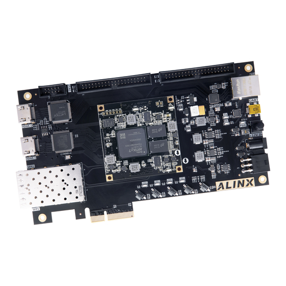
ARTIX-7 FPGA
Development Board
AX7203
User Manual
Table of
Contents
Previous
Page
Next
Page
1
2
3
4
5
Advertisement
Table of Contents
Need help?
Do you have a question about the ARTIX-7FPGA and is the answer not in the manual?
Ask a question
Questions and answers
Related Manuals for Alinx ARTIX-7FPGA
Motherboard Alinx ARTIX-7FPGA User Manual
(53 pages)
Motherboard Alinx ARTIX-7 FPGA User Manual
(59 pages)
Motherboard Alinx ARTIX-7 FPGA Manual
(30 pages)
Motherboard Alinx ARTIX-7 User Manual
(51 pages)
Motherboard Alinx AX7A200 Manual
Xilinx artix-7 fpga (59 pages)
Motherboard Alinx AX7A035 User Manual
(59 pages)
Motherboard Alinx AXU4EV-E User Manual
Zynq ultrascale+ fpga development board (58 pages)
Motherboard Alinx AV4075 User Manual
Fpga video processing development platform (56 pages)
Motherboard Alinx ZYNQ7000 FPGA User Manual
(54 pages)
Motherboard Alinx ZYNQ UltraScale+ User Manual
Fpga development board (66 pages)
Motherboard Alinx AX7101 User Manual
(51 pages)
Motherboard Alinx ZYNQ UltraScale+ AXU2CG-E User Manual
Fpga development board (56 pages)
Motherboard Alinx AXKU040 User Manual
Kintex ultrascale fpga development board (59 pages)
Motherboard Alinx AX7035 User Manual
Xilinx artix-7 fpga (42 pages)
Motherboard Alinx KINTEX UltraScale FPGA AXKU042 User Manual
(56 pages)
Motherboard Alinx AX7325 User Manual
Kintex-7fpga development board (48 pages)
This manual is also suitable for:
Ax7203
Table of Contents
Print
Rename the bookmark
Delete bookmark?
Delete from my manuals?
Login
Sign In
OR
Sign in with Facebook
Sign in with Google
Upload manual
Upload from disk
Upload from URL


Need help?
Do you have a question about the ARTIX-7FPGA and is the answer not in the manual?
Questions and answers