Table of Contents
Advertisement
Quick Links
Advertisement
Table of Contents

Subscribe to Our Youtube Channel
Related Manuals for Alinx AV4075


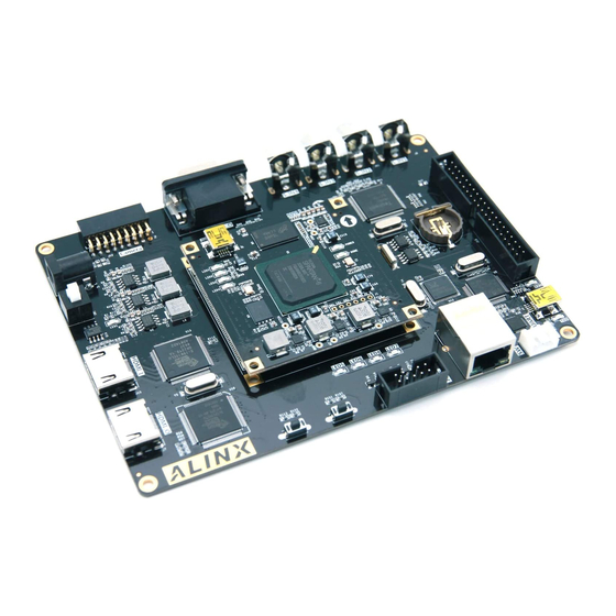
Summary of Contents for Alinx AV4075
- Page 1 FPGA Video Processing Development Platform AV4075 User Manual...
-
Page 2: Version Record
FPGA Video Processing Development Platform AV4075 User Manual Version Record Version Date Release By Description Rev 1.0 2019-05-01 Rachel Zhou First Release Amazon Store: https://www.amazon.com/alinx 2 / 56... -
Page 3: Table Of Contents
FPGA Video Processing Development Platform AV4075 User Manual Table of Contents Version Record ..................2 Part 1: FPGA Development Board Introduction ......... 6 Part 2: Function realization ................ 8 Part 2.1: Video Input ................8 Part 2.2: Video Output ............... 11 Part 3: AC4075 core board .............. - Page 4 FPGA Video Processing Development Platform AV4075 User Manual Part 4.11: Buttons ................53 Part 4.12: Power Supply ..............54 Amazon Store: https://www.amazon.com/alinx 4 / 56...
- Page 5 FPGA Video Processing Development Platform AV4075 User Manual Professional ALTERA FPGA Video Processing development platform (module: AV4075) adopts the core board + carrier board mode, which is convenient for users to use the core board for secondary development. This FPGA video image processing development platform is derived from the improvement of our company's ALTERA video development board AX822.
-
Page 6: Part 1: Fpga Development Board Introduction
FPGA Video Processing Development Platform AV4075 User Manual Part 1: FPGA Development Board Introduction The entire structure of the AV4075 FPGA development board is inherited from our consistent core board + carrier board model. A high-speed inter-board connector is used between the core board and the carrier board. - Page 7 FPGA Video Processing Development Platform AV4075 User Manual 视频 视频 视频 视频 HDMI输出 HDMI输入 VGA输出 输入 输入 输入 输入 接口 接口 接口 接口 ADV7123 SiI9134 TW2867 SiI9013 ALTERA EP4CE75F23 CP2102 RTL8211E 以太网网 CMOS接口 USB UART SD Card 口 Figure 1-1-1: The Schematic Diagram of the AV4075...
-
Page 8: Part 2: Function Realization
1-channel CMOS Input CMOS camera interface, can be connected to ALINX 5 megapixel OV5640 camera module On the FPGA carrier board, an ARM chip (STM32F103) is mounted on the board, and each interface chip and FPGA on the board are configured through I2C. - Page 9 FPGA Video Processing Development Platform AV4075 User Manual video sources available for development boards, such as: 1) Surveillance cameras Through the FPGA development board, it is possible to realize four-channel surveillance camera through the display (VGA/DVI/HDMI interface, which can realize 1080p) for split-screen display. Our development board is equivalent to the digital video host in the Figure below.
- Page 10 FPGA Video Processing Development Platform AV4075 User Manual Figure 2-1-2: Set top box 3) Camera Module CMOS camera interface, plug in ALINX 30 megapixel camera module or 5 megapixel camera module, real-time display 1080P video image on VGA display or HDMI display.
-
Page 11: Part 2.2: Video Output
FPGA Video Processing Development Platform AV4075 User Manual Part 2.2: Video Output There are two kinds of video output on the FPGA development board: you can connect a VGA monitor to display VGA images; you can also connect HMDI monitors or TV to display HDMI video signals. The video display for VGA and HDMI output is up to 1080P@60Hz. -
Page 12: Part 3: Ac4075 Core Board
FPGA Video Processing Development Platform AV4075 User Manual Part 3: AC4075 core board Amazon Store: https://www.amazon.com/alinx 12 / 56... -
Page 13: Part 3.1: Ac4075 Core Board Introduction
FPGA Video Processing Development Platform AV4075 User Manual Part 3.1: AC4075 Core Board Introduction FPGA+ 2DDR2 core board is based on ALTERA CYCLONE IV series EP4CE75F23C8. This chip develops a high-performance core board with high speed, high bandwidth and high capacity. It is suitable for video image processing and high-speed data acquisition. - Page 14 FPGA Video Processing Development Platform AV4075 User Manual Further, in order to allow DDR2 work properly, it is necessary to provide a reference voltage VREF and the termination voltage VTT is DDR2 DDR2 chip address lines and control lines, and VTT voltage VREF are 0.9V. Figure 3-2-1...
- Page 15 FPGA Video Processing Development Platform AV4075 User Manual AA20 DDR2_A[1] DDR2_A[12] DDR2_A[2] DDR2_BA[0] DDR2_A[3] DDR2_BA[1] AB10 DDR2_A[4] DDR2_BA[2] DDR2_A[5] DDR2_nCAS DDR2_A[6] DDR2_CKE AA19 DDR2_A[7] DDR2_CLK_P DDR2_A[8] DDR2_CLK_N AB18 DDR2_A[9] DDR2_DQ[16] DDR2_A[10] DDR2_DQ[17] DDR2_nRAS DDR2_DQ[18] AB16 DDR2_nWE DDR2_DQ[19] AA17 DDR2_ODT DDR2_DQ[20]...
-
Page 16: Part 3.3: Spi Flash
FPGA Video Processing Development Platform AV4075 User Manual Part 3.3: SPI Flash The AC4075 FPGA core board is equipped with one 64MBit SPI FLASH, and the model is M25P64, which uses the 3.3V CMOS voltage standard. Due to the non-volatile nature of SPI FLASH, it can be used as a boot device for the system to store the boot image of the system. -
Page 17: Part 3.4: Fpga Power Supply
FPGA Video Processing Development Platform AV4075 User Manual SPI Flash pin assignments: Pin Name FPGA Pin DCLK nCSO DATA0 ASDO Part 3.4: FPGA Power Supply In order for FGPA to work properly, we need to provide 3.3V, 1.8V, 2.5V, 1.2V and VCCIO five-way power for the FPGA. Let's talk about the power pin portion of the FPGA, which includes the power pins for each bank, the core voltage pins, the analog voltage, and the phase-locked loop power supply pins. - Page 18 FPGA Video Processing Development Platform AV4075 User Manual efficiency, small size, no heat, can provide large current, small ripple, etc. It is an excellent power solution for FPGA; a large number of high-grade imported capacitors are used to ensure the system's power supply is stable and reliable.
-
Page 19: Part 3.5: Expansion Ports
FPGA Video Processing Development Platform AV4075 User Manual The other two channels (3.3V and 2.5V) use less LDO chips SPX3819M5-L-3-3 and SPX3819M5-L-2-5 because of the low current required. Figure 3-4-2: LDO Power Supply Schematic Figure 3-4-3: Power Supply Circuit on the Core Board Part 3.5: Expansion Ports... - Page 20 FPGA Video Processing Development Platform AV4075 User Manual carrier board, which is configured for high speed data communication. Figure 3-5-1: Expansion Ports P1 Amazon Store: https://www.amazon.com/alinx 20 / 56...
- Page 21 FPGA Video Processing Development Platform AV4075 User Manual Figure 3-5-2: Expansion Ports P2 Amazon Store: https://www.amazon.com/alinx 21 / 56...
-
Page 22: Part 3.6: Powe Interface On Core Board
FPGA Video Processing Development Platform AV4075 User Manual Figure 3-5-3: Expansion Ports P1&P2 on the Core Board Part 3.6: Powe interface on Core Board In order to make the core board work normally, the FPGA expansion board needs to provide a +5V power supply to the core board through the expansion ports. -
Page 23: Part 3.7: Crystal Oscillator On Core Board
FPGA Video Processing Development Platform AV4075 User Manual Figure 3-6-1: Power input pin If you need to debug the core board separately, power the core board through the Mini USB port (J2) of the core board, the Mini USB cable is connected to the USB port of the computer. - Page 24 FPGA Video Processing Development Platform AV4075 User Manual Figure 3-7-1: Crystal oscillator Schematic Figure 3-7-2: Crystal oscillator on the Core Board Amazon Store: https://www.amazon.com/alinx 24 / 56...
-
Page 25: Part 3.8: Led Light On Core Board
FPGA Video Processing Development Platform AV4075 User Manual Crystal oscillator Pin Assignment Input Clock FPGA Pin 50MHz 27MHz Part 3.8: LED Light on Core Board There are 6 red LED lights on the AC4075 FPGA core board, one of which is the power indicator light (PWR), one is the configuration LED light (DONE), and four are the user LED light. - Page 26 FPGA Video Processing Development Platform AV4075 User Manual Figure 3-8-2: Power Indicator and Configure Indicator on the Core Board The schematic diagram of the four user LED sections is shown below. In Figure 3-8-3, When the FPGA pin output is logic 0, the LED will be lit.
- Page 27 FPGA Video Processing Development Platform AV4075 User Manual Figure 3-8-4: User LED on the Core Board User LEDs Pin Assignment LED Name FPGA Pin LED0 LED1 LED2 LED3 Amazon Store: https://www.amazon.com/alinx 27 / 56...
-
Page 28: Part 3.9: Structure Diagram
FPGA Video Processing Development Platform AV4075 User Manual Part 3.9: Structure Diagram Figure 3-9-1: AC4040 FPGA Core board (Top view) Figure 3-9-2: AC4040 FPGA Core board (Top view) Amazon Store: https://www.amazon.com/alinx 28 / 56... -
Page 29: Part 4: Carrier Board
FPGA Video Processing Development Platform AV4075 User Manual Part 4: Carrier Board Part 4.1: Carrier Board Introduction Through the previous function introduction, you can understand the function of the carrier board part 4-channel Video Input TW2867 1-channel HDMI Input SiI9013 ... -
Page 30: Part 4.2: Vga Display Interface
FPGA Video Processing Development Platform AV4075 User Manual With these hardware, you can complete the following experiments: Basic experiment 1) DDR3 test experiment 2) VGA output color bar experiment 3) HDMI output color bar experiment 4) TW2867 input to VGA display experiment... - Page 31 RGB digital signals to output VGA video signals, up to 1080p@60Hz output. In the AV4075 FPGA development board, the RGB digital signal output by the FPGA is 24-bit color, of which 8 colors are red, green and blue. In the schematic design, the 8-bit data of the red, green and blue output of the FPGA is connected to the 3-way DA of the ADV7123.
- Page 32 FPGA Video Processing Development Platform AV4075 User Manual Figure 4-2-2: VGA Display Interface on the Carrier Board VGA Signal Pin Assignment Pin Name FPGA Pin VGA_CLK VGA_EN VGA_HS VGA_VS VGA_R7 VGA_R6 VGA_R5 VGA_R4 VGA_R3 VGA_R2 VGA_R1 VGA_R0 VGA_G7 VGA_G6 VGA_G5...
-
Page 33: Part 4.3: Hdmi Output Interface
FPGA Video Processing Development Platform AV4075 User Manual VGA_G0 VGA_B7 VGA_B6 VGA_B5 VGA_B4 VGA_B3 VGA_B2 VGA_B1 VGA_B0 Part 4.3: HDMI Output Interface The HDMI output interface, used the SIL9134 HDMI (DVI) encoding chip of Silion Image , which supports up to 1080P@60Hz output and supports 3D output. - Page 34 FPGA Video Processing Development Platform AV4075 User Manual Figure 4-3-1: HDMI Output interafce Schematic Figure 4-3-2: HDMI Output interafce on the Carrier Board Amazon Store: https://www.amazon.com/alinx 34 / 56...
-
Page 35: Part 4.4: Hdmi Input Interface
FPGA Video Processing Development Platform AV4075 User Manual HDMI Output Interface Pin Assignment Pin Name FPGA Pin Description HDMI Output Clock 9134_CLK HDMI line sync signal 9134_HS HDMI column sync signal 9134_VS HDMI data valid signal 9134_DE Blue Data 0... - Page 36 FPGA Video Processing Development Platform AV4075 User Manual Image , which supports up to 1080P@60Hz input and Support data output in different formats. Among them, IIC interface of SIL9013 is connected with STM32F103, SIL9013 is initialized and controlled by STM32F103, and other pins of SIL9013 are connected to FPGA.
-
Page 37: Part 4.5: Video Input Interface
FPGA Video Processing Development Platform AV4075 User Manual HDMI Input Interface Pin Assignment Pin Name FPGA Pin Description HDMI Input Clock 9013_CLK HDMI line sync signal 9013_HS HDMI column sync signal 9013_VS HDMI data valid signal 9013_DE Blue Data 0... - Page 38 FPGA Video Processing Development Platform AV4075 User Manual PAL/NTSC/SECAM automatic identification, output BT656, multiplexable bus, FPGA-side demultiplexing, save IO Among them, the IIC interface and reset pin of TW2867 are connected to STM32F103, and the TW2867 is initialized and controlled by STM32F103.
-
Page 39: Part 4.6: Gigabit Ethernet Interface
FPGA Video Processing Development Platform AV4075 User Manual Figure 4-5-2: Video Input Interface on the Carrier Board Video Input Interface Pin Assignment Pin Name FPGA Pin 2867_CLKP 2867_CLKN 2867_D[0] 2867_D[1] 2867_D[2] 2867_D[3] 2867_D[4] 2867_D[5] 2867_D[6] 2867_D[7] Part 4.6: Gigabit Ethernet Interface... - Page 40 FPGA Video Processing Development Platform AV4075 User Manual The RTL8211EG chip supports 10/100/1000 Mbps network transmission rate and communicates with the FPGA through the GMII interface. RTL8211EG supports MDI/MDX adaptive, various speed adaptations, Master/Slave adaptation, and support for MDIO bus for PHY register management.
- Page 41 FPGA Video Processing Development Platform AV4075 User Manual Figure 4-6-1: Gigabit Ethernet Interface Schematic Figure 4-6-2: Gigabit Ethernet interface on the Carrier Board Amazon Store: https://www.amazon.com/alinx 41 / 56...
-
Page 42: Part 4.7: Arm Controller
FPGA Video Processing Development Platform AV4075 User Manual Gigabit Ethernet pin assignments: Pin Name FPGA Pin Description RGMII transmit clock E_GTXC Transmit Data bit0 E_TXD0 Transmit Data bit1 E_TXD1 Transmit Data bit2 E_TXD2 Transmit Data bit3 E_TXD3 Transmit enable signal... - Page 43 FPGA Video Processing Development Platform AV4075 User Manual Figure 4-7-1: ARM STM32F103 Schematic Figure 4-7-2: STM32F103 on the FPGA Board Amazon Store: https://www.amazon.com/alinx 43 / 56...
- Page 44 FPGA Video Processing Development Platform AV4075 User Manual At the same time, the ARM chip also brings out real-time clock, EEPROM, 4 LEDs, and serial ports. Part 4.7.1: Real Time Clock Figure 4-7-3: RTC Schematic Figure 4-7-4: RTC on the Carrier Board Amazon Store: https://www.amazon.com/alinx...
- Page 45 FPGA Video Processing Development Platform AV4075 User Manual ARM corresponding pin: Pin Name ARM Pin RTC_SCLK RTC_IO RTC_RESET Part 4.7.2: EEPROM Figure 4-7-5: EEPROM Schematic Figure 4-7-6: EEPROM on the Carrier Board Amazon Store: https://www.amazon.com/alinx 45 / 56...
- Page 46 FPGA Video Processing Development Platform AV4075 User Manual ARM corresponding pin: Pin Name ARM Pin 24LC04_SDA 24LC04_SCL Part 4.7.3: LED Figure 4-7-7: LED Schematic Figure 4-7-8: LED on the Carrier Board ARM corresponding pin: Pin Name ARM Pin LED0 LED1...
- Page 47 FPGA Video Processing Development Platform AV4075 User Manual Part 4.7.4: USB to Serial Port Figure 4-7-9: USB to Serial Port Schematic Figure 4-7-10: USB to Serial Port on the expansion port ARM corresponding pin: Pin Name ARM Pin RXD1 TXD1 Amazon Store: https://www.amazon.com/alinx...
- Page 48 FPGA Video Processing Development Platform AV4075 User Manual Part 4.7.5: SD Card Slot ARM communicates with the Micro SD card through the SPI interface for reading and storing SD card data. Figure 4-7-11: Mini SD Schematic Figure 4-7-12: SD Card Slot on the Carrier Board...
-
Page 49: Part 4.8: Camera Module Interface
FPGA Video Processing Development Platform AV4075 User Manual Part 4.8: Camera Module Interface The FPGA development board includes an 18-pin CMOS camera interface that can be connected to the OV5640 camera module for video capture. After acquisition, the monitor can be connected via HDMI or VGA interface for display. -
Page 50: Part 4.9: Expansion Header
Part 4.9: Expansion Header The Carrier Board is reserved with one 0.1inch spacing standard 40-pin expansion header J13 which is used to connect the ALINX modules or the external circuit designed by the user. The expansion port has 40 signals, of which 1-channel 5V power supply, 2-channel 3.3 V power supply, 3-channle... - Page 51 FPGA Video Processing Development Platform AV4075 User Manual Figure 4-9-1: Expansion header J13 schematic Figure 4-9-2: Expansion header J13 on the Carrier Board J13 Expansion Header Pin Assignment Pin Number FPGA Pin Pin Number FPGA Pin Amazon Store: https://www.amazon.com/alinx 51 / 56...
-
Page 52: Part 4.10: Jtag Interface
FPGA Video Processing Development Platform AV4075 User Manual D3V3 D3V3 Part 4.10: JTAG Interface A JTAG interface is reserved on the FPGA Carrier Board for downloading FPGA programs or firmware to FLASH. In order to prevent damage to the FPGA chip caused by hot plugging, a protection diode is added to the JTAG signal to ensure that the voltage of the signal is within the range accepted by the FPGA to avoid damage of the FPGA chip. - Page 53 FPGA Video Processing Development Platform AV4075 User Manual Figure 4-10-1: JTAG Interface Schematic Figure 4-10-2: JTAG Interface on the Carrier Board Be careful not to hot swap when JTAG cable is plugged and unplugged. Part 4.11: Buttons The FPGA carrier board contains two user buttons KEY1~KEY2. All buttons are connected to the normal IO of the FPGA.
- Page 54 FPGA Video Processing Development Platform AV4075 User Manual Figure 4-11-1: Button Schematic Figure 4-11-2: User Buttons on the Carrier Board Buttons Pin Assignment Net Name FPGA PIN KEY1 KEY2 Part 4.12: Power Supply The power input voltage of the FPGA development board is DC5V. It is converted into D3V3, D1V2, D1V8 three-way power supply through three-way DC/DC power chip MP1482.
- Page 55 FPGA Video Processing Development Platform AV4075 User Manual Figure 4-12-1 Power Design Schematic on the Carrier Board Amazon Store: https://www.amazon.com/alinx 55 / 56...
- Page 56 FPGA Video Processing Development Platform AV4075 User Manual Figure 4-12-2: Power Supply circuit on the Carrier Board Amazon Store: https://www.amazon.com/alinx 56 / 56...
Need help?
Do you have a question about the AV4075 and is the answer not in the manual?
Questions and answers