Table of Contents
Advertisement
Quick Links
Introduction
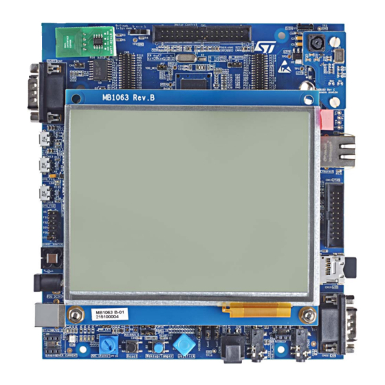
The STM32746G-EVAL evaluation board is a complete demonstration and development
platform for STMicroelectronics ARM
microcontroller. It features four I
interfaces, SDMMC, four USARTs, four UARTs, two CANs, three 12-bit ADCs, two 12-bit
DACs, two SAIs, 8 to 14-bit digital camera module interface, internal 320+4-Kbyte SRAM
and 1-Mbyte Flash memory, USB HS OTG and USB FS OTG, Ethernet MAC, FMC
interface, Quad-SPI interface, JTAG debugging support. This evaluation board can be used
as a reference design for user application development but it is not considered as a final
application.
The full range of hardware features on the board helps the user to evaluate all peripherals
(USB OTG HS, USB OTG FS, Ethernet, Motor control, CAN, microSD card, USART, Audio
DAC and ADC, digital microphone, IrDA, RF-EEPROM, SRAM, Nor Flash memory,
SDRAM, Quad-SPI Flash memory, 5.7" TFT LCD with a capacitive touch panel and others)
and to develop his applications. Extension headers make it possible to easily connect a
daughterboard for a specific application.
The integrated ST-LINK/V2-1 provides an embedded in-circuit debugger and programmer
for the STM32.
1. Picture not contractual.
March 2016
All manuals and user guides at all-guides.com
Evaluation board with STM32F746NG MCU
®
Cortex
2
C interfaces, six SPIs with three multiplexed simplex I
Figure 1. STM32746G-EVAL evaluation board
DocID027916 Rev 2
User manual
®
-M7 core-based STM32F746NGH6
UM1902
2
S
1/79
www.st.com
1
Advertisement
Table of Contents

Related Manuals for ST User Manual


Summary of Contents for ST User Manual
- Page 1 SDRAM, Quad-SPI Flash memory, 5.7" TFT LCD with a capacitive touch panel and others) and to develop his applications. Extension headers make it possible to easily connect a daughterboard for a specific application. The integrated ST-LINK/V2-1 provides an embedded in-circuit debugger and programmer for the STM32. Figure 1. STM32746G-EVAL evaluation board 1.
-
Page 2: Table Of Contents
Embedded ST-LINK/V2-1 ........10... - Page 3 TFT LCD connector CN20 ........45 6.19 ST-LINK/V2-1 USB Type B connector CN21 ..... . 46 6.20 CAN D-type 9-pin male connector CN22 .
- Page 4 All manuals and user guides at all-guides.com Contents UM1902 D.1.1 FCC Compliance Statement ........77 Part 15.19 .
- Page 5 All manuals and user guides at all-guides.com UM1902 List of tables List of tables Table 1. Power related jumpers ........... . 13 Table 2.
- Page 6 STM32746G-EVAL ST-LINK/V2-1 ........
-
Page 7: Features
• STM32F746NGH6 microcontroller with 1-Mbyte Flash memory and 320+4-Kbyte RAM • Six 5 V power supply options: – Power jack – ST-LINK/V2-1 USB connector – User USB HS connector – User USB FS1 connector – User USB FS2 connector –... -
Page 8: Demonstration Software
For more information and to download the latest version available, refer to the STM32746G-EVAL demonstration software available on www.st.com. Ordering information To order the evaluation board for STM32F746NGH6 MCU, use the order code: STM32746G-EVAL2. -
Page 9: Hardware Layout And Configuration
SRAM, Nor Flash memory, QSPI Flash memory , Camera module, Color LCD, USB OTG connectors, Motor control connector, USART, IrDA, Ethernet, Audio, CAN, RF-EEPROM, microSD card and embedded ST-LINK/V2-1). Figure 2. Hardware block diagram 1. The red circles show the I/O shared among the default functions and the camera or the motor control connectors. -
Page 10: Embedded St-Link/V2-1
Joystick Button onnector Button Embedded ST-LINK/V2-1 The ST-LINK/V2-1 programming and debugging tool is embedded on the STM32746G- EVAL evaluation board. Compared to ST-LINK/V2 the changes are listed below. The new features supported on ST-LINK/V2-1 are: • USB software re-enumeration •... -
Page 11: Drivers
The ST-LINK/V2-1 embeds a firmware upgrade mechanism for in-situ upgrade through the USB port. As the firmware may evolve during the life time of the ST-LINK/V2-1 product (for example new functionalities, bug fixes, support for new microcontroller families), it is recommended to visit www.st.com... -
Page 12: Power Supply
5 V DC power with 300 mA limitation from CN21, the USB type B connector of ST-LINK/V2-1 (USB 5 V power source on silkscreen of JP13 (STlk)). If the USB enumeration succeeds (as explained below), the ST-LINK/V2-1 U5V power is enabled, by asserting the PWR_EN pin. -
Page 13: Table 1. Power Related Jumpers
All manuals and user guides at all-guides.com UM1902 Hardware layout and configuration The following power sequence procedure must be respected: • Connect jumper JP13 for PSU or D5V side • Check that JP15 is removed • Connect the external power source to PSU or D5V (daughterboard mounted) •... - Page 14 Table 1. Power related jumpers (continued) Jumper Description For power supply from USB connector of ST-LINK/V2-1 (CN21) to STM32746G- EVAL only, JP13 is set as shown to the right: For power supply from the daughterboard connectors (CN5 and CN6) to...
-
Page 15: Clock Source
All manuals and user guides at all-guides.com UM1902 Hardware layout and configuration Table 1. Power related jumpers (continued) Jumper Description For power supply from USB OTG HS (CN8) to STM32746G-EVAL only, JP13 is set as shown to the right: JP13 For power supply from power supply jack(CN17) to both STM32746G-EVAL and daughterboard connected on CN5 and CN6, JP13 is set as shown to the right (daughterboard must not have its own power supply connected):... -
Page 16: Reset Source
Debugging Tools from JTAG/SWD connector CN15 and ETM trace connector CN12 • Daughterboard from CN5 • Embedded ST-LINK/V2-1 • RS232 connector CN7 for ISP Note: The jumper JP3 has to be closed for RESET handled by the pin 8 of the RS232 connector CN7 (CTS signal). -
Page 17: Boot Option
Boot address Switch configuration Boot space option bytes STM32746G-EVAL boot from BOOT_ADD0[15:0] 0<->1 BOOT_ADD0 [15:0] ST programmed value: Flash memory on ITCM at 0x0020 0000 (Default setting). STM32746G-EVAL boot from 0<->1 BOOT_ADD1[15:0] BOOT_ADD1 [15:0] ST programmed value: System bootloader at 0x0010 0000 Table 5. -
Page 18: Table 6. Audio Related Jumpers
All manuals and user guides at all-guides.com Hardware layout and configuration UM1902 connectors CN24 and CN27 can be used to support MEMS microphone evaluation board STEVAL-MKI129V1 after removing SB20 and SB21. An optical connector CN28, compatible with SPDIF spec, is implemented on STM32746G- EVAL, to receive external audio data. - Page 19 All manuals and user guides at all-guides.com UM1902 Hardware layout and configuration Table 6. Audio related jumpers (continued) Jumper Description PD6 is as FMC_NWAIT signal when JP5 is set as shown to the right (Default setting): PD6 is connected to digital microphone as I2S data signal when JP5 is set as shown to the right (it is also needed to set JP18 together according to this table): Digital microphone power source is connected to +3.3 V power when JP17 is set as shown to the right (Default setting):...
-
Page 20: Usb Otg Fs1
All manuals and user guides at all-guides.com Hardware layout and configuration UM1902 USB OTG FS1 STM32746G-EVAL evaluation board supports USB OTG full speed communication via a USB Micro-AB connector (CN13) and USB power switch (U11) connected to VBUS. The evaluation board can be powered by this USB connection at 5 V DC with 500 mA current limitation. -
Page 21: Rs232 And Irda
STM32746G-EVAL evaluation board. The signal Bootloader_RESET and Bootloader_BOOT are added on RS232 connector CN7 for ISP support. USART1 of the STM32F746NGH6 microcontroller is shared with RS232/IrDA and ST- LINK/V2-1 controller. Its communication can be changed by setting JP14 and JP20. -
Page 22: Rf-Eeprom
All manuals and user guides at all-guides.com Hardware layout and configuration UM1902 5.11 RF-EEPROM RF-EEPROM daughterboard ANT7-M24LR-A is mounted on CN2 of the STM32F746NGH6 microcontroller via I2C1 bus. The RF-EEPROM can be accessed by the microcontroller via the I2C1 bus or by Radio Frequency (RF), using a 13.56 MHz reader (for example, CR95HF). -
Page 23: Memories
All manuals and user guides at all-guides.com UM1902 Hardware layout and configuration Table 10. Ethernet related jumpers Jumper Description 25 MHz clock is provided by external crystal X4 when JP6 is set as shown to the right (Default setting): 25 MHz clock for MII is provided by MCO at PA8 when JP6 is set as shown to the right: Table 11. -
Page 24: Quad-Spi Nor Flash Memory
All manuals and user guides at all-guides.com Hardware layout and configuration UM1902 Table 12. NOR Flash memory related jumpers Jumper Description Write protection is enabled when JP10 is fitted while write protection is disabled when JP10 is not fitted. JP10 Default setting: Not fitted Description of JP5 is in Section 5.6: Audio... -
Page 25: Display And Input Devices
All manuals and user guides at all-guides.com UM1902 Hardware layout and configuration 5.18 Display and input devices 4-general-purpose-color leds (LD 1,2,3,4) are available for the display device and they are connected on MFX. Table 13. LED related jumpers Jumper Description PB7 is connected to LED3(red) when JP23 is set as shown to the right (Default setting): JP23... -
Page 26: Figure 5. Orientation Setting Of The 5.7-Inch Lcd Daughterboard
All manuals and user guides at all-guides.com Hardware layout and configuration UM1902 Table 14. LCD modules connector (CN20) (continued) Pin No. Description Pin connection Pin No. Description Pin connection PJ12 PJ13 PJ14 HSYNC PI12 PJ15 VSYNC PI13 PI14 RESET# I2C1_SDA MFX GPIO14 I2C1_SCL BL_CTRL... -
Page 27: Motor Control
All manuals and user guides at all-guides.com UM1902 Hardware layout and configuration 5.19 Motor control STM32746G-EVAL evaluation board supports both asynchronous and synchronous three- phase brushless motor control via a 34-pin connector CN1, which provides all required control and feedback signals to and from motor power-driving board. The available signals on this connector are emergency stop, motor speed, 3 phases motor current, bus voltage, heatsink temperature, coming from the motor driving board and 6 channels of PWM control signal, going to the motor driving circuit. -
Page 28: Mfx (Multi-Function Expander)
All manuals and user guides at all-guides.com Hardware layout and configuration UM1902 Figure 7. STM32746G-EVAL evaluation board motor control PCB reworks (Top side) 1. To remove R95 and R100, open SB5 and mount R14 Table 15. Motor control related solder bridges Solder Description Bridges... - Page 29 All manuals and user guides at all-guides.com UM1902 Hardware layout and configuration Table 16. MFX signals (continued) Pin name of Functions of Direction Terminal number MFX functions STM32746G-EVAL (For MFX) device of MFX MFX_GPIO5 Audio_INT Input Codec OTG_FS1_ MFX_GPIO6 Input USB_FS1 OverCurrent OTG_FS1_...
-
Page 30: Connector
All manuals and user guides at all-guides.com Connector UM1902 Connector Motor control connector CN1 Figure 8. Motor control connector CN1 (Top view) Table 17. Motor control connector CN1 Pins of the Pins of the Description number number Description STM32F746NGH6 STM32F746NGH6 of CN1 of CN1 Emergency... -
Page 31: Rf-Eeprom Daughterboard Connector Cn2
All manuals and user guides at all-guides.com UM1902 Connector RF-EEPROM daughterboard connector CN2 Figure 9. RF-EEPROM daughterboard connector CN2 (Front view) Table 18. RF-EEPROM daughterboard connector CN2 Pin number Description Pin number Description I2C1_SDA (PB9) +3V3 I2C1_SCL (PB8) RESET(PC10) Analog input connector CN3 Figure 10. -
Page 32: Camera Module Connector Cn4
All manuals and user guides at all-guides.com Connector UM1902 Camera module connector CN4 Figure 11. Camera module connector CN4 (Top view) Table 20. Camera module connector CN4 Pin number Description Pin number Description +1.8V +1.8V D0(PC6) D1(PC7) D10(PD6) D2(PC8) D11(PD2) D3(PC9) D4(PC11) D5(PD3) -
Page 33: Daughterboard Extension Connector Cn5 And Cn6
(CN10 and CN11), and on connectors CN5 and CN6. The space between CN5 and CN6 connectors is defined as a standard, this allows developing common daughterboards for several ST evaluation boards. The standard width between CN5 pin1 and CN6 pin1 is 2700 mils (68.58 mm). - Page 34 All manuals and user guides at all-guides.com Connector UM1902 Table 21. Daughterboard extension connector CN5 (continued) How to disconnect with function Description Alternative Function block on STM32746G-EVAL board MII_MDIO_GPIO Open SB11 LCD_G0 PJ10 LCD_G3 LCD_G1 PI11 ULPI_DIR Remove R124 ULPI_D7 Remove R119 OSC_OUT Remove C23,X1, Close SB28...
-
Page 35: Table 22. Daughterboard Extension Connector Cn6
All manuals and user guides at all-guides.com UM1902 Connector Table 21. Daughterboard extension connector CN5 (continued) How to disconnect with function Description Alternative Function block on STM32746G-EVAL board LCD_R2 Table 22. Daughterboard extension connector CN6 How to disconnect with function block on Description Alternative Function STM32746G-EVAL board... - Page 36 All manuals and user guides at all-guides.com Connector UM1902 Table 22. Daughterboard extension connector CN6 (continued) How to disconnect with function block on Description Alternative Function STM32746G-EVAL board PC11 SDCARD_D3 /PAR_D4 Remove R275, Disconnect CN4 SDCARD_D2/EXT_RESET/P PC10 Remove R16,R281, Disconnect CN4 AR_D8 SDCARD_CMD/PAR_D11 Open SB63, Disconnect CN4...
-
Page 37: Rs232 Connector Cn7
All manuals and user guides at all-guides.com UM1902 Connector Table 22. Daughterboard extension connector CN6 (continued) How to disconnect with function block on Description Alternative Function STM32746G-EVAL board MC_VH/PAR_D1/MIC_CK Disconnect CN1,CN4, Keep JP19 on open Open SB62, Disconnect CN4, Keep JP4 on MC_UH/PAR_D0/I2S3_CK open RS232 connector CN7... -
Page 38: Usb Otg Hs Micro-Ab Connector Cn8
All manuals and user guides at all-guides.com Connector UM1902 USB OTG HS Micro-AB connector CN8 Figure 13. USB OTG HS Micro-AB connector CN8 (Front view) Table 24. USB OTG HS Micro-AB connector CN8 Pin number Description Pin number Description VBUS Ethernet RJ45 connector CN9 Figure 14. -
Page 39: Memory Connector Cn10 And Cn11
All manuals and user guides at all-guides.com UM1902 Connector Memory connector CN10 and CN11 Two 40-pin male headers CN10 and CN11 are used to connect with memory daughterboard. GPIOs (which work as FMC memory signals) that are not present on CN5 and CN6, are available on these two connectors. -
Page 40: Table 27. Memory Connector Cn11
All manuals and user guides at all-guides.com Connector UM1902 Table 26. Memory connector CN10 (continued) How to disconnect with function block on Description Alternative function STM32746G-EVAL board PE11 PF15 PE14 PH10 A14/BA0 PH12 PD10 PD15 SDCLK/ MII_PPS_OUT Table 27. Memory connector CN11 How to disconnect with function block on Description Alternative function... - Page 41 All manuals and user guides at all-guides.com UM1902 Connector Table 27. Memory connector CN11 (continued) How to disconnect with function block on Description Alternative function STM32746G-EVAL board PH13 SDCKE0 A21/TRACED2/PAR_D6 Open SB3,SB4 NWAIT /I2S3_SD/PAR_D10 Set JP5 on pin1-2, Disconnect CN4 A23/TRACECLK/ MII_TXD3 Open SB7, Remove R247 PH15...
-
Page 42: Etm Trace Debugging Connector Cn12
All manuals and user guides at all-guides.com Connector UM1902 6.10 ETM Trace debugging connector CN12 Figure 15. ETM Trace debugging connector CN12 (Top view) Table 28. ETM Trace debugging connector CN12 Pin number Description Description number +3.3V TMS/PA13 TCK/PA14 TDO/PB3 TDI/PA15 RESET# TraceCLK/PE2... -
Page 43: Usb Otg Fs2 Micro-Ab Connector Cn14
All manuals and user guides at all-guides.com UM1902 Connector Table 29. USB OTG FS1 Micro-AB connector CN13 Pin number Description Pin number Description VBUS (PA9) ID (PA10) D- (PA11) D+ (PA12) 6.12 USB OTG FS2 Micro-AB connector CN14 Figure 17. USB OTG FS2 Micro-AB connector CN14 (Front view) Table 30. -
Page 44: Microsd Connector Cn16
All manuals and user guides at all-guides.com Connector UM1902 Table 31. JTAG/SWD debugging connector CN15 Pin number Description Pin number Description +3.3V +3.3V PA15 PA13 PA14 RTCK RESET# DBGRQ DBGACK 6.14 MicroSD connector CN16 Figure 19. MicroSD connector CN16 (Top view) Table 32. -
Page 45: Power Connector Cn17
Figure 20. Power supply connector CN17 (Front view) 6.16 ST-LINK/V2-1 programming connector CN18 The connector CN18 is used only for embedded ST-LINK/V2-1 programming during board manufacturing. It is not populated by default and not for end user. 6.17 MFX programming connector CN19 The connector CN19 is used only for MFX (Multi-Function eXpander) programming during board manufacturing. -
Page 46: St-Link/V2-1 Usb Type B Connector Cn21
UM1902 6.19 ST-LINK/V2-1 USB Type B connector CN21 The USB connector CN21 is used to connect the embedded ST-LINK/V2-1 to PC to debug the board. Figure 21. USB type B connector CN21 (Front view) Table 33. USB type B connector CN21... -
Page 47: Mems Microphone Coupon Connectors Cn24 And Cn27
All manuals and user guides at all-guides.com UM1902 Connector 6.21 MEMS microphone coupon connectors CN24 and CN27 Figure 23. MEMS microphone coupon connectors CN24 and CN27 (Top view) Table 35. MEMS microphone coupon connectors CN24 and CN27 Pin number Description Pin number Description DATA... -
Page 48: Spdif In Connector Cn28
All manuals and user guides at all-guides.com Connector UM1902 6.24 SPDIF IN connector CN28 Figure 24. SPDIF IN connector CN28 (Front view) Table 36. SPDIF IN connector CN28 Pin number Description Pin number Description SPDIF_RX1(PG12) 48/79 DocID027916 Rev 2... -
Page 49: Appendix A Electrical Schematics
All manuals and user guides at all-guides.com Appendix A Electrical schematics Figure 25. STM32746G-EVAL evaluation board U_MCU U_Memory MCU.SchDoc Same length Memory.SchDoc R190 +3V3 I2C1_SCL A[0..23] A[0..23] R191 I2C1_SDA D[0..31] D[0..31] U_Audio 90MHz clock SDCLK SDCLK Audio.SchDoc SDNE0 SDNE0 I2C1_SCL SAI2_SCKB SAI2_SCKB SDNRAS... -
Page 50: Figure 26. Stm32746G-Eval Mcu
All manuals and user guides at all-guides.com Figure 26. STM32746G-EVAL MCU SB34 Open MC_EnA SB36 Open MII_CRS SB32 Closed SAI2_SDB SB23 Open MC_EnB SB29 Closed MII_RX_CLK ULPI_STP SB30 Open Open SB31 MC_EnIndex MC_CurrentA MII_MDIO MII_MDC SB24 Closed Closed SB22 SAI2_SCKB SAI1_SDA JP21 JP22... -
Page 51: Figure 27. Stm32746G-Eval Power
All manuals and user guides at all-guides.com Figure 27. STM32746G-EVAL Power ZEN056V130A24LS CN17 220uF DC-10B SMAJ5.0A-TR 100nF BNX002-01 +3V3 VDD_MCU C127 [N/A] C104 [N/A] [N/A] [N/A] JP13 VBUS_HS VBUS_FS1 TP14 TP13 TP16 +3V3 LD1117S18TR +1V8 VBUS_FS2 LD10 Ground Ground Ground Ground Vout R142... -
Page 52: Figure 28. Stm32746G-Eval Sram, Flash Memory And Dram
All manuals and user guides at all-guides.com Figure 28. STM32746G-EVAL SRAM, Flash memory and DRAM D[0..31] D[0..31] A[0..23] A[0..23] DQ31 DQ30 I/O15 DQ15A-1 DQ29 I/O14 DQ14 DQ28 I/O13 DQ13 DQ27 I/O12 DQ12 DQ26 I/O11 DQ11 DQ25 I/O10 DQ10 DQ24 I/O9 DQ23 I/O8 DQ22... -
Page 53: Figure 29. Stm32746G-Eval Audio
All manuals and user guides at all-guides.com Figure 29. STM32746G-EVAL Audio +3V3 LDO1VDD AGND Default I2C Address:0011010 +3V3 AVDD1 AGND SPKVDD1 AGND +1V8 SPKVDD2 SPKGND1 AVDD2 SPKGND2 +1V8 CPVDD CPGND +3V3 DCVDD DGND DBVDD HP2GND +1V8 LDO2VDD R189 I2C1_SDA R188 R195 +3V3 LDO1ENA... -
Page 54: Figure 30. Stm32746G-Eval Lcd, Camera And Rf Connector
All manuals and user guides at all-guides.com Figure 30. STM32746G-EVAL LCD, Camera and RF connector RGB LCD Camera CN20 LCD_R[0..7] PI15 LCD_R0 LCD_G0 LCD_G[0..7] LCD_R[0..7] LCD_G[0..7] LCD_R1 LCD_G1 PAR_D[0..11] PAR_D[0..11] LCD_R2 LCD_G2 LCD_R3 LCD_G3 PJ10 LCD_R4 LCD_G4 PJ11 +1V8 C103 C102 11 12 LCD_R5... -
Page 55: Figure 31. Stm32746G-Eval Ethernet
All manuals and user guides at all-guides.com Figure 31. STM32746G-EVAL Ethernet +3V3 R131 100nF R120 R114 100nF MII_TX_CLK TX_CLK PG11 MII_TX_EN TX_EN PG13 MII_TXD0 TXD_0 PG14 MII_TXD1 TXD_1 MII_TXD2 TXD_2 MII_TXD3 TXD_3/SNI_MODE MII_RXD0 RXD_0/PHYAD1 MII_RXD1 RXD_1/PHYAD2 LED(green)_A MII_RXD2 RXD_2/PHYAD3 LED(green)_K MII_RXD3 RXD_3/PHYAD4 LED(Yellow)_A... -
Page 56: Figure 32. Stm32746G-Eval Usb Otg Hs And Otg Fs2
All manuals and user guides at all-guides.com Figure 32. STM32746G-EVAL USB OTG HS and OTG FS2 +3V3 R135 CN14 PB13 VBUS_FS2 VBUS PB14 R288 USB_FS2_DM PB15 R286 USB_FS2_DP PB12 USB_FS2_ID Green Vbus D+out D+in Shield D-out D-in Shield R138 Shield 9013 Shield 475900001... -
Page 57: Figure 33. Stm32746G-Eval Usb Otg Fs1
All manuals and user guides at all-guides.com Figure 33. STM32746G-EVAL USB OTG FS1 +3V3 R133 MFX_GPIO6 OTG_FS1_OverCurrent R134 To MFX R132 CN13 FAULT VBUS MFX_GPIO7 R130 OTG_FS1_PowerSwitchOn From MFX STMPS2151STR 4.7uF R129 Shield Shield Shield Shield 475900001 +3V3 VBUS_FS1 PA11 R284 USB_FS1_DM PA12... -
Page 58: Figure 34. Stm32746G-Eval Rs232 And Irda
All manuals and user guides at all-guides.com Figure 34. STM32746G-EVAL RS232 and IrDA +3V3 C135 C136 100nF 100nF DB9-male USART1 C134 100nF 100nF 100nF T1IN T1OUT RS232/IrDA_TX T2IN T2OUT T3IN T3OUT R1OUTB Bootloader_BOOT0 R2OUTB R1OUT R1IN R2OUT R2IN R3OUT R3IN PA10 RS232/IrDA_RX Bootloader_RESET... -
Page 59: Figure 35. Stm32746G-Eval Can And Qspi
All manuals and user guides at all-guides.com Figure 35. STM32746G-EVAL CAN and QSPI +3V3 R163 R168 +3V3 C166 CN22 Default setting: 1<->2 DB9-male CAN connector Default setting: Open JP11 100nF PA12 JP12 CAN1_TX CANH CANL PA11 CAN1_RX Vref R164 SN65HVD230 ESDCAN24-2BLY R170 R174... -
Page 60: Figure 36. Stm32746G-Eval Peripherals
All manuals and user guides at all-guides.com Figure 36. STM32746G-EVAL Peripherals Wakeup Button Potentiometer +3V3 R218 two pin header for external analog input +3V3 C100 WKUP/TAMPER PF10 Potentiometer 100nF [N/A] R29 0 3386P-103(10K) R216 PC13 [N/A] TAMPER_WKUP_KEY R217 220K Close to MCU on PCB +3V3 MICRO SD Joystick... -
Page 61: Figure 37. Stm32746G-Eval Motor Control
All manuals and user guides at all-guides.com Figure 37. STM32746G-EVAL Motor control +3V3 Motor control connector MC_EmergencySTOP EMERGENCY STOP [N/A] MC_UH MC-UH MC_UL MC_UL MC_VH MC_VH MC_VL MC_VL MC_WH MC_WH MC_WL MC_WL BUS VOLTAGE MC_BusVoltage MC_CurrentA CURRENT A CURRENT B 100nF 100K CURRENT C... -
Page 62: Figure 38. Stm32746G-Eval Extension Connector
All manuals and user guides at all-guides.com Figure 38. STM32746G-EVAL Extension connector Place close Memory CN10 SDNE0 SDNWE PF13 PF14 PF12 PF11 SDNRAS SB27 Left Right Open PI11 PI13 SB26 SB25 11 12 SB28 PC15 PC14 PE10 13 14 R224 Open PI15 PC13... -
Page 63: Figure 39. Stm32746G-Eval St-Link/V2-1
All manuals and user guides at all-guides.com Figure 39. STM32746G-EVAL ST-LINK/V2-1 VBUS_HS +3V3_ST_LINK BAT60JFILM R209 R208 VBUS_FS1 BAT60JFILM BAT60JFILM U16 LD3985M33R +3V3_ST_LINK C167 C169 C174 C172 JP15 VBUS_FS2 Vout 100nF 100nF 100nF 100nF +3V3_ST_LINK BAT60JFILM BYPASS R173 1uF_X5R_0603 1uF_X5R_0603 BAT60JFILM... -
Page 64: Figure 40. Stm32746G-Eval Mfx
All manuals and user guides at all-guides.com Figure 40. STM32746G-EVAL MFX R299 PF10 LED1 +3V3 Green R207 [N/A] Multi Function eXpander Orange +3V3 +3V3 +3V3 one capacitor close to each MFX pins: R206 VDD, VDD_1, VDD_2, VDD_3 R300 Ferrite LED3 C171 C176 C170... -
Page 65: Figure 41. Stm32746G-Eval Jtag And Trace
All manuals and user guides at all-guides.com Figure 41. STM32746G-EVAL JTAG and Trace +3V3 R141 R143 R136 R137 [N/A] [N/A] [N/A] [N/A] PA13 TMS/SWDIO PA14 TCK/SWCLK TDO/SWO R101 PA15 R112 TRST R104 RESET# R140 [N/A] Trace connector JTAG connector CN15 CN12 +3V3 JTAG... -
Page 66: Figure 42. Stm32746G-Eval Camera Daughterboard
All manuals and user guides at all-guides.com Figure 42. STM32746G-EVAL Camera daughterboard +1V8 100nF 100nF +2V8 11 12 13 14 15 16 Camera_RST 17 18 STANDBY EXTCLK 19 20 +2V8 +2V8 +2V8 21 22 Camera_CLK PAR_D0 PAR_D1 MCLK AVDD(2.8V) 23 24 PAR_PCLK [N/A] PAR_D2... -
Page 67: Figure 43. Stm32746G-Eval 5.7 Tft Lcd Daughterboard
All manuals and user guides at all-guides.com Figure 43. STM32746G-EVAL 5.7 TFT LCD daughterboard [N/A] BLGND DCLK HSYNC HSYNC VSYNC VSYNC [N/A] BL_CTRL 11 12 13 14 VLED 15 16 BLVDD VLED 17 18 VLED 19 20 21 22 4.7uF 23 24 100nF 100nF... -
Page 68: Appendix B Stm32746G-Eval I/O Assignment
All manuals and user guides at all-guides.com STM32746G-EVAL I/O assignment UM1902 Appendix B STM32746G-EVAL I/O assignment Table 37. I/O assignment STM32746G-EVAL Camera Motor control variant name standard variant A20/TRACED1 A19/TRACED0 A23/TRACECLK/MII_TXD3 PG14 MII_TXD1 NBL1 NBL0 Audio and EXPANDER and ACP and RF_I2C1_SCL ULPI_D7 NJTRST... - Page 69 All manuals and user guides at all-guides.com UM1902 STM32746G-EVAL I/O assignment Table 37. I/O assignment (continued) STM32746G-EVAL Camera Motor control variant name standard variant PA12 CAN1_TX/USB_FS1_DP PFC_SYNC2_TIM1_ETR PI8- ANTI EXPANDER_INT TAMP2 NBL2 LCD_DE LCD_B7 LCD_B6 PG12 SPDIF_RX1 PG10 PJ14 LCD_B2 PA11 CAN1_RX/USB_FS1_DM PFC_PWM_TIM1_1_CH4...
- Page 70 All manuals and user guides at all-guides.com STM32746G-EVAL I/O assignment UM1902 Table 37. I/O assignment (continued) STM32746G-EVAL Camera Motor control variant name standard variant RS232_IRDA_USART1_RX/USB_FS1_ PA10 PC14- OSC32_I OSC32_IN PI12 LCD_HSYNC PDR_ON - BOOT BOOT VDD_3 VDD_11 VDD_10 VDD_15 VCAP2 PH13 PH14 RS232_IRDA_USART1_TX/...
- Page 71 All manuals and user guides at all-guides.com UM1902 STM32746G-EVAL I/O assignment Table 37. I/O assignment (continued) STM32746G-EVAL Camera Motor control variant name standard variant LCD_G6 LCD_G7 SDCARD_D1 PFC_SYNC1_TIM1_1_CH Backlight_PWM_TIM1_CH1 /MII_MCO PH0 - OSC_IN OSC_IN PI13 LCD_VSYNC PI15 LCD_R0 VDD_18 VSS_17 VSS_9 VDDUSB - PJ11...
- Page 72 All manuals and user guides at all-guides.com STM32746G-EVAL I/O assignment UM1902 Table 37. I/O assignment (continued) STM32746G-EVAL Camera Motor control variant name standard variant SDNE0/MII_COL VDD_12 VSS_12 VSS_8 VDD_8 LCD_G0 LCD_G2 MII_MDC(GPIO) MII_MDIO(GPIO) QSPI_BK1_IO2 QSPI_BK1_IO3 SDCKE0 VDD_4 VSS_4 VSS_6 VSS_7 VSS_1 VSS_14 VDD_14...
- Page 73 All manuals and user guides at all-guides.com UM1902 STM32746G-EVAL I/O assignment Table 37. I/O assignment (continued) STM32746G-EVAL Camera Motor control variant name standard variant VDD_1 VCAP1 PD14 PB12 ULPI_D5/USB_FS2_ID VSSA ULPI_STP CURRENT_A_ADC1_123_ SAI1_SD_A/MII_MDC IN11 CURRENT_B_ADC2_123_ MII_TXD2 IN12 QSPI_CLK PF12 PF15 LCD_R5 PD12 PD13...
- Page 74 All manuals and user guides at all-guides.com STM32746G-EVAL I/O assignment UM1902 Table 37. I/O assignment (continued) STM32746G-EVAL Camera Motor control variant name standard variant PD11 A15(BA1) A14(BA0) MII_RXD3 PH11 VREF+ SAI2_SCK_B/MII_MDIO INDEX_TIM5_5_CH3 STOP_TIM8_BKIN PIXCLK ULPI_CK DAC_OUT2 MII_RXD1 HEATSINK_ADC12_IN15 PF14 LCD_R3 PF11 SDNRAS PE11...
- Page 75 All manuals and user guides at all-guides.com UM1902 STM32746G-EVAL I/O assignment Table 37. I/O assignment (continued) STM32746G-EVAL Camera Motor control variant name standard variant PB11 ULPI_D4 PB14 USB_FS2_DM PB15 USB_FS2_DP DocID027916 Rev 2 75/79...
-
Page 76: Appendix C Mechanical Dimensions
All manuals and user guides at all-guides.com Mechanical dimensions UM1902 Appendix C Mechanical dimensions Figure 44. Mechanical dimensions Table 38. Mechanical dimensions Symbol Size (mm) Symbol Size (mm) Symbol Size (mm) 68.58 114.18 24.43 48.62 116.5 16.94 1.27 55.37 21.36 46.77 32.64 9.98... -
Page 77: Appendix D Compliance Statement
All manuals and user guides at all-guides.com UM1902 Compliance statement Appendix D Compliance statement Federal Communications Commission (FCC) and Industry Canada (IC) Compliance Statements D.1.1 FCC Compliance Statement Part 15.19 This device complies with Part 15 of the FCC Rules. Operation is subject to the following two conditions: (1) this device may not cause harmful interference, and (2) this device must accept any interference received, including interference that may cause undesired operation. -
Page 78: Table 39. Document Revision History
All manuals and user guides at all-guides.com Revision History UM1902 Revision History Table 39. Document Revision History Date Version Revision Details 10-Jun-2015 Initial release. 16-Mar-2016 Added Section Appendix D: Compliance statement. 78/79 DocID027916 Rev 2... - Page 79 ST products and/or to this document at any time without notice. Purchasers should obtain the latest relevant information on ST products before placing orders. ST products are sold pursuant to ST’s terms and conditions of sale in place at the time of order acknowledgement.
Need help?
Do you have a question about the User Manual and is the answer not in the manual?
Questions and answers