Table of Contents
Advertisement
Quick Links
UM2248
User manual
Evaluation board with STM32L4R9AI MCU
Introduction
The STM32L4R9I-EVAL board is designed as complete demonstration and development
®
®
platform for the STMicroelectronics Arm
Cortex
-M4 core-based STM32L4R9AI
microcontroller with four I²C buses, three SPI and six USART ports, CAN port, two SAI
ports, 12-bit ADC, 12-bit DAC, internal 640-Kbyte SRAM and 2-Mbyte Flash memory, two
Octo-SPI memory interfaces, touch-sensing capability, USB OTG FS port, LCD-TFT
®
controller, MIPI
DSI host controller, flexible memory controller (FMC), 8- to 14-bit camera
interface and JTAG debugging support.
The STM32L4R9I-EVAL, shown in
Figure
3,
Figure
4, and
Figure
5, is used as a reference
design for user application development before porting to the final product.
The full range of hardware features on the board helps the user to evaluate all the
peripherals (USB, USART, digital microphones, ADC and DAC, TFT LCD, MIPI DSI
display, LDR, SRAM, NOR Flash memory device, Octo-SPI Flash memory device,
microSD™ card, sigma-delta modulators, CAN transceiver, EEPROM) and develop
applications. Extension headers allow easy connection of a daughterboard or wrapping
board for a specific application.
An ST-LINK/V2-1 is integrated on the board, as the embedded in-circuit debugger and
programmer for the STM32 MCU and the USB virtual COM port bridge.
October 2017
DocID030791 Rev 2
1/87
www.st.com
1
Advertisement
Table of Contents

Subscribe to Our Youtube Channel
Related Manuals for ST STM32L4R9I-EVAL


Summary of Contents for ST STM32L4R9I-EVAL
-
Page 1: User Manual
Extension headers allow easy connection of a daughterboard or wrapping board for a specific application. An ST-LINK/V2-1 is integrated on the board, as the embedded in-circuit debugger and programmer for the STM32 MCU and the USB virtual COM port bridge. -
Page 2: Table Of Contents
Hardware layout and configuration ......11 STM32L4R9I-EVAL board views ....... 13 Mechanical dimensions . - Page 3 STM32L4R9I-EVAL used as USB device ..... . . 26 9.10.2 STM32L4R9I-EVAL used as USB host ......26 9.10.3 Limitations in using USB OTG FS port .
- Page 4 10.16 TFT LCD connector CN20 (RGB) ......61 10.17 ST-LINK/V2-1 USB Micro-B connector CN21 ..... 61...
- Page 5 UM2248 Contents 10.18 CAN D-type male connector CN22 ......62 Electrical schematics ........63 Appendix A I/O assignment .
- Page 6 STM32L4R9I-EVAL I/O assignment ........
- Page 7 STM32L4R9I-EVAL hardware block diagram ........11...
-
Page 8: Features
PMOD connector • Board expansion connectors: – Motor-control connector – Extension connector for daughterboard • Flexible power-supply options: power jack, ST-LINK/V2-1 USB connector, USB OTG FS connector, daughterboard • On-board ST-LINK/V2-1 debugger/programmer with USB re-enumeration capability: 8/87 DocID030791 Rev 2... -
Page 9: Product Marking
ST is not responsible for any consequences resulting from such use. In no event will ST be liable for the customer using any of these engineering samples tools as reference design or in production. -
Page 10: Demonstration Software
MCU, is preloaded in the STM32 Flash memory for easy demonstration of the device peripherals in standalone mode. The latest versions of the demonstration source code and associated documentation are available from www.st.com. Ordering information To order the evaluation board based on the STM32L4R9AII6 MCU, use the order code STM32L4R9I-EVAL. -
Page 11: Hardware Layout And Configuration
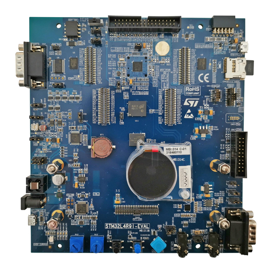
Figure Figure 4, and Figure 5 are the three images showing the STM32L4R9I-EVAL board top view with round DSI display, top view with TFT LCD, and bottom view. Figure 1. STM32L4R9I-EVAL hardware block diagram DocID030791 Rev 2 11/87... -
Page 12: Figure 2. Stm32L4R9I-Eval Board (Top Side)
Hardware layout and configuration UM2248 Figure 2. STM32L4R9I-EVAL board (top side) 12/87 DocID030791 Rev 2... -
Page 13: Stm32L4R9I-Eval Board Views
UM2248 Hardware layout and configuration STM32L4R9I-EVAL board views Figure 3. STM32L4R9I-EVAL board (top view) with round DSI display MB1314 daughterboard Picture is not contractual DocID030791 Rev 2 13/87... -
Page 14: Figure 4. Stm32L4R9I-Eval Board (Top View) With Tft Lcd Mb1315 Daughterboard
Hardware layout and configuration UM2248 Figure 4. STM32L4R9I-EVAL board (top view) with TFT LCD MB1315 daughterboard Picture is not contractual 14/87 DocID030791 Rev 2... -
Page 15: Figure 5. Stm32L4R9I-Eval Board (Bottom View)
UM2248 Hardware layout and configuration Figure 5. STM32L4R9I-EVAL board (bottom view) Picture is not contractual DocID030791 Rev 2 15/87... -
Page 16: Mechanical Dimensions
Hardware layout and configuration UM2248 Mechanical dimensions Figure 6. MB1313 STM32L4R9I-EVAL board 16/87 DocID030791 Rev 2... -
Page 17: St-Link/V2-1
Hardware layout and configuration Figure 7. MB1314 DSI display daughterboard ST-LINK/V2-1 ST-LINK/V2-1 facility for debug and flashing of STM32L4R9AII6, is integrated on the STM32L4R9I-EVAL board. Compared to ST-LINK/V2 stand-alone tool available from STMicroelectronics, ST-LINK/V2- 1 offers new features and drops some others. -
Page 18: Drivers
9.3.1 Drivers Before connecting STM32L4R9I-EVAL to a Windows (XP, 7, 8 10) PC via USB, a driver for ST-LINK/V2-1 must be installed. It is available from www.st.com. In case the STM32L4R9I-EVAL board is connected to the PC before installing the driver, the Windows device manager may report some USB devices found on STM32L4R9I-EVAL as “Unknown”. -
Page 19: Power Supply
NOR Flash memory usable capacity is reduced to 16 Mbits. Power Supply The STM32L4R9I-EVAL board is designed to be powered from 5 V DC power source. It incorporates a precise polymer Zener diode (Poly-Zen) protecting the board from damage due to wrong power supply. One of the following four 5 V DC power inputs is usable with an appropriate board configuration: •... -
Page 20: Supplying The Board Through St-Link/V2-1 Usb Port
EVAL from the power source. In the next phase of the enumeration procedure, the host PC informs the ST-LINK/V2-1 facility of its capability to supply up to 300 mA of current. If the answer is positive, the ST-LINK/V2-1 sets the U22 ST890 switch to ON position to supply power to the remainder of the STM32L4R9I-EVAL board. -
Page 21: Table 2. Power Supply Related Jumpers Settings
STM32L4R9I-EVAL is supplied through CN18 power jack (marked PSU_DC5V). CN5 and CN6 extension connectors do not pass the 5 V of STM32L4R9I-EVAL to daughterboard. STM32L4R9I-EVAL is supplied through CN3 Micro-AB USB connector. CN5 and CN6 extension connectors do not pass the 5 V of STM32L4R9I-EVAL to daughterboard. -
Page 22: Clock References
CN21 using USB charger. 1. On all ST-LINK/V2-1 boards, the target application is now able to run even if the STLINK/V2-1 is either not connected to an USB host, or is powered through a USB charger (or through a not-enumerating USB host). -
Page 23: Reset Sources
PH1 OSC_OUT is routed to extension connector CN5. Resistor Closed R65 must be removed, in order not to disturb clock reference or source on daughterboard. Reset sources The reset signal of STM32L4R9I-EVAL board is active low. Sources of reset are listed below: • reset button B2 •... -
Page 24: Bootloader Limitations
Bootloader version is identified by reading the Bootloader ID at the address 0x1FFF6FFE: the content is 0x91 for bootloader V9.1 and 0x92 for V9.2. The STM32L4R9AII6 part soldered on the STM32L4R9I-EVAL main board is marked with a date code corresponding to its date of manufacturing. STM32L4R9AII6 parts with a date code prior or equal to week 37 of 2017 are fitted with bootloader V9.1 affected by the... -
Page 25: Audio
WA3: Using bootloader, load a patch code in RAM to write in Flash memory through same Write Memory write protocol as bootloader (code provided by ST). The patch code is available for download from www.st.com... -
Page 26: Headphones Outputs
The resistor R23 must be left open to prevent STM32L4R9I-EVAL from sourcing 5 V to VBUS terminal, which would cause conflict with the 5 V sourced by the USB host. This may happen if the MFX_GPIO6 is controlled by the software of the MFX MCU such that, it enables the output of U2 power switch. -
Page 27: Limitations In Using Usb Otg Fs Port
The CN8 slot for microSD card is routed to STM32L4R9AII6 SDIO port, accepting SD (up to 2 Gbytes) and SDHC (up to 32 Gbytes) cards. One 8-Gbyte microSD card is delivered as part of STM32L4R9I-EVAL. The card insertion switch is routed to the MFX_GPIO5 of MFX MCU port. -
Page 28: Motor Control
Hardware layout and configuration UM2248 9.13 Motor control The CN1 connector is designed to receive a motor-control (MC) module. Table 7 shows the assignment of CN1 and STM32L4R9AII6 terminals. Table 7 also lists the modifications to be made on the board versus its by-default configuration. - Page 29 UM2248 Hardware layout and configuration Table 7. Motor-control terminal and function assignment (continued) Motor-control STM32L4R9AII6 microcontroller connector CN1 Alternate Terminal Port Board modifications for Terminal Function name name enabling motor control function Close SB37. PhaseB ADC1_IN2 current+ Remove R244. PhaseB current- Close SB43.
-
Page 30: Board Modifications To Enable Motor Control
Hardware layout and configuration UM2248 Table 7. Motor-control terminal and function assignment (continued) Motor-control STM32L4R9AII6 microcontroller connector CN1 Alternate Terminal Port Board modifications for Terminal Function name name enabling motor control function Close SB17. Remove SB18. Encoder B TIM4_CH2 ADC12_IN Remove R30 or no daughterboard. -
Page 31: Figure 9. Pcb Top-Side Rework For Motor Control
UM2248 Hardware layout and configuration Figure 9. PCB top-side rework for motor control DocID030791 Rev 2 31/87... -
Page 32: Figure 10. Pcb Bottom-Side Rework For Motor Control
Hardware layout and configuration UM2248 Figure 10. PCB bottom-side rework for motor control 32/87 DocID030791 Rev 2... -
Page 33: Can
CAN_TX is used from STM32L4R9AII6 termina.l 9.14.1 Limitations CAN operation is exclusive with Audio codex and MC operation. 9.14.2 Operating voltage The supply voltage for STM32L4R9I-EVAL CAN operation must be within the range from 3.0 V to 3.6 V. DocID030791 Rev 2 33/87... -
Page 34: Extension Connectors Cn5, Cn6, Cn13 And Cn14
Each LED is in light-emitting state with low level of the corresponding ports of STM32L4R9AII6. And the four LEDs are exclusive with MC operation. 9.17 Physical input devices The STM32L4R9I-EVAL board provides a number of input devices for physical human control, listed below: • four-way joystick controller with select key (B1) •... -
Page 35: Limitations
Operational amplifier STM32L4R9AII6 provides two on-board operational amplifiers, one of which, OpAmp1, is made accessible on STM32L4R9I-EVAL. OpAmp1 has its inputs and its output routed to I/O ports PA0, PA1 and PA3, respectively. The non-inverting input PA0 is accessible on the terminal 1 of the JP5 jumper header. -
Page 36: Comparator
STM32L4R9AII6 provides two on-board comparators, one of which, Comp2, is made accessible on STM32L4R9I-EVAL. Comp2 has its non-inverting input and its output routed to I/O ports PB4 and PB5, respectively. The input is accessible on the terminal 3 of the JP5 jumper header. -
Page 37: Limitations
IS61WV102416BLL, a 16-Mbit static RAM (SRAM), 1 M x 16 bit, is fitted on the STM32L4R9I-EVAL main board, in U17 position. The STM32L4R9I-EVAL main board, as well as the addressing capabilities of FMC, allow hosting SRAM devices up to 64 Mbytes. This is... -
Page 38: Limitations
NOR Flash memory device M29W128GL70ZA6E, a 128-Mbit NOR Flash memory, 8 M x16 bit, is fitted on the STM32L4R9I-EVAL main board, in U11 position. The STM32L4R9I-EVAL main board, as well as the addressing capabilities of FMC, allow hosting M29W256GL70ZA6E, a 256-Mbit NOR Flash memory device. -
Page 39: Operating Voltage
M24128-DFDW6TP, a 128-Kbit I²C-bus EEPROM device, is fitted on the main board of STM32L4R9I-EVAL, in U3 position. It is accessed with I²C-bus lines I2C2_SCL and I2C2_SDA of STM32L4R9AII6. It supports all I²C-bus modes with speeds up to 1 MHz. The base I²C-bus address is 0xA0. -
Page 40: Limitations
2.7 V to 3.6 V. 9.25 Octo-SPI DRAM device IS66WVH8M8BLL-100BLI, a 64-Mbit self-refresh dynamic RAM (DRAM) device with a HyperBus interface, is fitted on the STM32L4R9I-EVAL main board, in U5 position. It allows evaluating STM32L4R9AII6 Octo-SPI interface. 9.25.1 Operating voltage Voltage of Octo-SPI DRAM device IS66WVH8M8BLL-100BLI is in the range of 2.7 V to... -
Page 41: Table 15. Touch-Sensing-Related Configuration Elements
UM2248 Hardware layout and configuration touch sensing performance, by isolating copper tracks to avoid disturbances due to their antenna effect. Table 15. Touch-sensing-related configuration elements Element Setting Configuration PC6 port is routed to CN6 connector for daughterboard. This setting is not good for robustness of touch sensing. Default setting. -
Page 42: Limitations
MFX MCU The MFX MCU is used as MFX (multi function expander) and IDD measurement. The MFX circuit on STM32L4R9I-EVAL board acts as IO-expander. The communication interface between MFX and STM32L4R9AII6 is I2C2 bus. The signals connected to MFX are... -
Page 43: Idd Measurement
MCU supply voltage (VDD_MCU line) does not exceed 3.3 V. This is because there are components on STM32L4R9I-EVAL supplied from 3.3 V that communicate with the MCU through I/O ports. Voltage exceeding 3.3 V on the MCU output port may inject current into 3.3 V-supplied peripheral I/Os and false the MCU current... -
Page 44: Limitations
Hardware layout and configuration UM2248 Table 18. DSI display module connector CN16 (continued) Pin No. Description Pin connection Pin No. Description Pin connection DSI_D0_P DSI_D0_N DSI_D1_P DSI_D1_N BLVDD (5 V) SPI_CS PG12 BLVDD (5 V) SPI_CLK/UART_CK PI1/PG13 SPI_SDI/UART_TX PI3/PB6 BLGND SPI_DCX BLGND SCLK/MCLK... -
Page 45: Limitations
UM2248 Hardware layout and configuration mount on STM32L4R9I-EVAL board with RGB mode. Table 19 shows the assignment of CN20 and STM32L4R9AII6 terminals. Table 19. TFT LCD module connector CN20 RGB mode FMC mode RGB mode FMC mode description description connection... -
Page 46: Pmod Connector
UM2248 9.31 PMOD connector The standard PMOD connector P1 is available on STM32L4R9I-EVAL board to support flexibility in small form factor application. The PMOD connector is implemented the PMOD type 2A and 4A on STM32L4R9I-EVAL board. Table 20. PMOD connector P1... -
Page 47: Mb1315 Tft Lcd Board
MB1315 TFT LCD board MB1315 is TFT LCD daughterboard supporting RGB mode, available to mount on STM32L4R9I-EVAL board via connector CN1. The 4.3” TFT LCD is used LCD RK043FN48H-CT672B with capacitive touch panel which only supports 3.3 V power and interface. So a level shifter SN74LVC16T245DGGR is requested on TFT RGB LCD daughterboard to support wide power supply range. - Page 48 Hardware layout and configuration UM2248 Table 22. MB1315 board connector CN1 pin function description (continued) Pin number Description Pin number Description LCD_DSIP HSYNC VSYNC PCLK RST# BL_CTRL BL+5 V BLGND BLGND +3.3 V 48/87 DocID030791 Rev 2...
-
Page 49: Connectors
UM2248 Connectors Connectors 10.1 Motor-control connector CN1 Figure 11. Motor-control connector CN1 (top view) Table 23. Motor-control connector CN1 Pin of Pin of Description number number Description STM32L4R9AII6 STM32L4R9AII6 of CN1 of CN1 Emergency STOP PWM_1H PWM_1L PH13 PWM_2H PWM_2L PH14 PWM_3H PWM_3L... -
Page 50: External I 2 C Connector Cn2
Connectors UM2248 10.2 External I C connector CN2 Figure 12. EXT_I2C connector CN2 (front view) Table 24. EXT_I2C connector CN2 Pin number Description Pin number Description I2C1_SDA (PH5) I2C_SCL (PH4) EXT_RESET (MFX_GPIO8) 10.3 USB OTG FS Micro-AB connector CN3 Figure 13. USB OTG FS Micro-AB connector CN3 (Front view) Table 25. -
Page 51: Analog Input-Output Connector Cn4
UM2248 Connectors 10.4 Analog input-output connector CN4 Figure 14. Analog input-output connector CN4 (top view) Table 26. Analog input-output connector CN4 Pin number Description Pin number Description Analog input-output PA4 10.5 Extension connectors CN5, CN6, CN13 and CN14 All GPIO signals from STM32L4R9AII6 are connected to extension connectors CN5, CN6, CN13 and CN14. -
Page 52: Table 28. Daughter Board Extension Connector Cn6
Connectors UM2248 Table 27. Daughter board extension connector CN5 (continued) How to disconnect alternative functions to Description Alternative functions number use on the extension connector PH10 OCTO-SPI2_IO5 Remove the U5. OCTO-SPI2_NCS Remove the U5. PH12 OCTO-SPI2_IO7 Remove the U5. OCTO-SPI2_CLK Remove the U5. - Page 53 UM2248 Connectors Table 28. Daughter board extension connector CN6 (continued) How to disconnect alternative functions to Description Alternative functions number use on the extension connector LPUART1_RX Remove the U9. VBUS_FS, MC Remove R203, open SB35. SDIO1_D1, Trace_D0 Remove R205, open SB57. TS_KEY_CS, MC Closed R46, open SB19 and SB20.
-
Page 54: Table 29. Daughter Board Extension Connector Cn13
Connectors UM2248 Table 28. Daughter board extension connector CN6 (continued) How to disconnect alternative functions to Description Alternative functions number use on the extension connector OCTO-SPI1_NCS Remove the U6. Table 29. Daughter board extension connector CN13 How to disconnect alternative functions to Description Alternative functions number... -
Page 55: Table 30. Daughter Board Extension Connector Cn14
UM2248 Connectors Table 29. Daughter board extension connector CN13 (continued) How to disconnect alternative functions to Description Alternative functions number use on the extension connector FMC_A22 Keep the CN12 open. FMC_A0 DFSDM, MC Remove R242, open SB36. SAI1, MC Remove R244, open SB37. FMC_A3 FMC_A14 FMC_A11... - Page 56 Connectors UM2248 Table 30. Daughter board extension connector CN14 (continued) How to disconnect alternative functions to Description Alternative functions number use on the extension connector PE14 FMC_D11 PE15 FMC_D12 Do not use the CN11, CN12, CN15, CN17 for PA13 JTAG_TMS/SWDIO debug connector.
-
Page 57: Rs232 Connector Cn7
UM2248 Connectors 10.6 RS232 connector CN7 Figure 15. RS232 D-sub male connector (front view) Table 31. RS232 D-sub male connector Pin number Description Description number RS232_RX (PG8) RS232_RTS (PB12) RS232_TX (PG7) RS232_CTS (PB13) 10.7 microSD connector CN8 Figure 16. microSD connector CN8 (top view) DocID030791 Rev 2 57/87... -
Page 58: Mfx Programming Connector Cn9
Connectors UM2248 Table 32. microSD connector CN8 Description Description number number SDIO_D2 (PC10) Vss/GND SDIO_D3 (PC11) SDIO_D0 (PC8) SDIO_CMD (PD2) SDIO_D1 (PC9) SDIO_CLK (PC12) MicroSDcard_detect (MFX GPIO15) 10.8 MFX programming connector CN9 The connector CN9 is used only for embedded MFX (multi function expander) programming during board manufacture. -
Page 59: Trace Debugging Connector Cn12
UM2248 Connectors 10.10 Trace debugging connector CN12 Figure 18. ETM trace debugging connector CN12 (Top view) Table 34. Trace debugging connector CN12 Description Description number number +3.3 V TMS/PA13 TCK/PA14 TDO/PB3 TDI/PA15 RESET# Trace_CLK/PE2 Trace_D0/PE3 or SWO/PB3 Trace_D1/PE4 or nTRST/PB4 Trace_D2/PE5 Trace_D3/PE6 10.11... -
Page 60: Dsi Display Connector Cn16 (Mipi)
Connectors UM2248 10.12 DSI display connector CN16 (MIPI) A TFT color LCD with MIPI DSI interface board is mounted on CN16. Refer to Section 9.29 detail. 10.13 JTAG connector CN17 Figure 19. JTAG/SWD debugging connector CN17 (Top view) Table 36. JTAG/SWD debugging connector CN17 Description Description number... -
Page 61: Power Connector Cn18
UM2248 Connectors 10.14 Power connector CN18 The STM32L4R9I-EVAL board is power-able with a DC 5 V power supply via the external power supply jack (CN18) shown in Figure 20. The central pin of CN18 must be positive. Figure 20. Power-supply connector CN18 (front view) 10.15... -
Page 62: Table 38. Can D-Type 9-Pin Male Connector Cn22
Connectors UM2248 Table 37. USB Micro-B connector CN21 (front view) (continued) Pin number Description Pin number Description Shield 10.18 CAN D-type male connector CN22 Figure 22. CAN D-type 9-pin male connector CN22 (front view) Table 38. CAN D-type 9-pin male connector CN22 Pin number Description Pin number... -
Page 63: Electrical Schematics
UM2248 Electrical schematics Electrical schematics This section provides design schematics for the STM32L4R9I-EVAL key features to help users to implement these features in application designs. This section includes: • Overall schematics for the STM32L4R9I-EVAL, see Figure 23 • STM32L4R9I-EVAL MCU, see Figure 24 •... -
Page 64: Figure 23. Overall Schematics For The Stm32L4R9I-Eval
Figure 23. Overall schematics for the STM32L4R9I-EVAL U_MCU U_MotorControl U_DSI LCD MCU.SchDoc MotorControl.SchDoc DSI LCD.SchDoc MC_CurrentA MC_CurrentA USART1_CK USART1_CK MC_CurrentB MC_CurrentB USART1_TX USART1_TX MC_CurrentC MC_CurrentC SWIRE SWIRE MC_PFC_IndCurr MC_PFC_IndCurr U_IDD_measurement DSI_BL_CTRL DSI_BL_CTRL MC_BusVoltage MC_BusVoltage IDD_measurement.SchDoc MC_Temperature MC_Temperature Same length 500MHz clock... -
Page 65: Figure 24. Stm32L4R9I-Eval Mcu
Figure 24. STM32L4R9I-EVAL MCU SB36 MC_CurrentA SB38 R242 MC_PFC_IndCurr DFSDM_DATA4 R214 SB37 MFX_IRQ_OUT MC_CurrentB SB39 R244 OpAmp1_INP SAI1_SDA SB40 SB43 MC_Temperature MC_CurrentC R216 R217 OpAmp1_INM LCD_INT SB54 MC_PFC_Vac PA0-WKUP OCTOSPI1_IO6 R215 SB55 OpAmp1_VOUT MC_BusVoltage R221 OCTOSPI1_CLK OCTOSPI1_NCS OCTOSPI1_IO7 PA[0..15] TKEY PA[0..15]... -
Page 66: Figure 25. Power Supply
Figure 25. Power supply connected by shunt of IDD_measurement circuitry VDD_MCU +3V3 ZEN056V130A24LS VDD_ADJ TP11 CN18 JP10 VDD_IO 220uF VDD_IO DC-10B VDD_MCU Header 2X1 100nF BNX002-01 ESDA7P60-1U1M VDDIO2 VDDA VDDIO2 VDDA VDD_MCU VDDA VSSA/VREF- +3V3 VREF+ VREF+ BEAD(FCM1608KF-601T03) C118 C120 DSI_VCAP VCAPDSI VSSDSI... -
Page 67: Figure 26. Sram And Nor Flash Memory Devices And Tft Lcd
Figure 26. SRAM and NOR Flash memory devices and TFT LCD D[0..15] D[0..15] A[0..23] A[0..23] CN20 PF14 DQ15A-1 PF15 DQ14 PE15 DQ13 PE10 I/O15 DQ12 PE11 I/O14 DQ11 PD10 PE12 I/O13 DQ10 PD11 PE13 I/O12 PD12 PE14 I/O11 I/O10 PF11 I/O9 DE/TE LCD_DE... -
Page 68: Figure 27. Audio Codec Device
Figure 27. Audio codec device +3V3 I2C address: 0x34 LDO1VDD AGND +3V3 AVDD1 AGND SPKVDD1 AGND +1V8 SPKVDD2 SPKGND1 AVDD2 SPKGND2 +1V8 CPVDD CPGND DCVDD DGND DBVDD HP2GND +1V8 LDO2VDD R159 I2C_SDA R166 R165 LDO1ENA SCLK I2C_SCL R164 [N/A] LDO2ENA CS/ADDR VREFC CIFMODE... -
Page 69: Figure 28. Dsi Display Connector
Figure 28. DSI display connector DSI LCD CN16 DSI_CK_P DSI_INT DSI_CK_N DSI_D2_P SB28 DSI_D2_N SB27 DSI_D0_P DSI_D0_N DSI_D3_P SB31 DSI_D3_N SB30 DSI_D1_P DSI_D1_N PG12 SPI_CS PG13 USART1_CK SB25 C134 SPI_CLK BEAD(FCM1608KF-601T03) C135 10uF USART1_TX 100nF SB24 SPI_SDI SPI_DCX BEAD(FCM1608KF-601T03) USART1_CK/TX config SB on MCU sheet SCLK/MCLK +3V3 LRCLK... -
Page 70: Figure 29. Physical Control Peripherals, Microsd Card And Eeprom
Figure 29. Physical control peripherals, microSD card and EEPROM MICRO SD (TF) Card Buttons LEDs SDIO1_D1 SDIO1_D0 PC11 SDIO1_D3 PC10 SDIO1_D2 R190 PC12 +3V3 Green SDIO1_CLK R187 PB15 LED1 SDIO1_CMD Orange R186 PH13 C103 WKUP LED2 [N/A] EMIF06-HSD03F3 R188 PC13 R185 PH14 WAKEUP... -
Page 71: Figure 30. Analog Input And Output And Touch-Sensing Device
Figure 30. Analog input and output and touch-sensing device Comp2_INP Comp2_INP Header 2X1 Default setting: Open Comp2_OUT Comp2_OUT ADC_DAC [N/A] 3386P-103(10K) Close to MCU on PCB Default setting: 1<->2 from Potentiometer ADC&DAC connector COMP2_OUT STM32L Potentiometer Comparator Comp2_INP Comp2 Comp2_OUT R118 8.2K Default setting: 2<->3 to Comp2... -
Page 72: Figure 31. St-Link/V2-1
Figure 31. ST-LINK/V2-1 +3V3_ST_LINK +3V3_ST_LINK CN19 R161 R160 STM_JTMS_SWDIO VBUS_FS STM_JTCK_SWCLK BAT60JFILM BAT60JFILM LDK120M33R +3V3_ST_LINK C136 C139 C142 C140 C137 Vout 4.7uF 100nF 100nF 100nF 100nF SB33 [N/A] +3V3_ST_LINK BAT60JFILM BYPASS VUSB_ST_LINK R162 1uF_X5R_0603 1uF_X5R_0603 BAT60JFILM 100K +3V3_ST_LINK 100nF 10nF_X7R_0603... -
Page 73: Figure 32. Idd Measurement
Figure 32. IDD measurement R123 BEAD(FCM1608KF-601T03) VDD1 VDD1 C126 C127 100nF GPIO0 JOY_SEL SPARE GPIO1 JOY_DOWN MFX_IRQ_OUT MFX_IRQ_OUT GPIO2 JOY_LEFT TSC_XP/GPO0 GPIO3 JOY_RIGHT NRST BAT60JFILM MFX_aGPIO1 NRST TSC_XN/GPO1 GPIO4 JOY_UP TSC_YP/GPO2 GPIO5 uSD_Detect TSC_YN/GPO3 GPIO6 USB_PSON GPIO7 USB_OVRCR Capacitor close to MCU R133 BOOT0 GPIO8... -
Page 74: Figure 33. Jtag And Trace Debug Connectors
Figure 33. JTAG and trace debug connectors CN15 PA13 PA13 TMS/SWDIO PA14 PA15 TCK/SWCLK PA14 TDO/SWO PA15 R104 TRST Tag-10_C RESET# R139 Only footprint with Cable: TC2050-IDC-NL [N/A] Trace connector JTAG connector CN17 CN12 JTAG R144 [N/A] R143 R102 [N/A] R103 [N/A] R145... -
Page 75: Figure 34. Motor-Control Connector
Figure 34. Motor-control connector +3V3 Motor control connector MC_EmergencySTOP EMERGENCY STOP MC_PWM_1H PWM_1H PH13 MC_PWM_1L PWM_1L MC_PWM_2H PWM_2H PH14 MC_PWM_2L PWM_2L MC_BusVoltage MC_PWM_3H PWM_3H PH15 MC_PWM_3L PWM_3L BUS VOLTAGE 100nF 100K MC_CurrentA PHASE A CURRENT + PHASE A CURRENT - PHASE B CURRENT + PHASE B CURRENT - PHASE C CURRENT +... -
Page 76: Figure 35. Usb Otg Fs Port
Figure 35. USB OTG FS port +3V3 MFX_GPIO7 USB_OVRCR To MFX FAULT VBUS MFX_GPIO6 USB_PSON From MFX STMPS2151STR 4.7uF Shield Shield Shield Shield 475900001 Hirose: ZX62RD-AB-5P8 +3V3 VBUS_FS PA11 USBOTG_DM PA12 USBOTG_DP PA10 USBOTG_ID I/O1 I/O4 Vbus I/O2 I/O3 Green USBLC6-4SC6 9013 USB Full Speed operating range voltage: 3.0V<VDDUSB<3.6V... -
Page 77: Figure 36. Usart, Can Transceiver And Pmod Connector
Figure 36. USART, CAN transceiver and PMOD connector USART +3V3 DB9-male C106 C105 100nF 100nF C107 100nF 100nF 100nF UART_RTS_3V3 T1IN T1OUT UART_TX_3V3 T2IN T2OUT T3IN T3OUT R1OUTB R2OUTB R1OUT R1IN UART_RX UART_RX_3V3 R2OUT R2IN R3OUT R3IN PB13 UART_CTS UART_CTS_3V3 R4OUT R4IN R5OUT... -
Page 78: Figure 37. Octo-Spi Flash Memory Device
Figure 37. Octo-SPI Flash memory device R212 [N/A] OCTOSPI1_CLK SCLK OCTOSPI1_NCS OCTOSPI1_DQS OCTOSPI1_IO0 SIO0 C5 for VPP from Mircon OCTOSPI1_IO1 SIO1 OCTOSPI1_IO2 SIO2 OCTOSPI1_IO3 SIO3 OCTOSPI1_IO4 SIO4 VCCQ PG11 R202 OCTOSPI1_IO5 SIO5 VCCQ [N/A] OCTOSPI1_IO6 SIO6 C111 C109 C116 OCTOSPI1_IO7 SIO7 100nF 100nF... -
Page 79: Figure 38. Extension Connectors
Figure 38. Extension connectors Place close Memory Left CN13 PH14 PH12 PH15 PG15 PG10 PH13 11 12 11 12 PG13 PG12 13 14 13 14 15 16 15 16 PI10 17 18 17 18 PI11 19 20 19 20 21 22 21 22 PC14 SB50... -
Page 80: Table 39. Stm32L4R9I-Eval I/O Assignment
I/O assignment UM2248 Appendix A I/O assignment Table 39. STM32L4R9I-EVAL I/O assignment Primary UFBGA RGB LCD with Motor-control Pin name Pinout assignment 169 DSI FMC mode connector DSI_CKN DSI_CKP DSI_D0N DSI_D0P DSI_D1N DSI_D1P VCAPDSI [L13] VDD12DSI [L13] VDD12DSI VSSDSI VSSDSI... - Page 81 UM2248 I/O assignment Table 39. STM32L4R9I-EVAL I/O assignment (continued) Primary UFBGA RGB LCD with Motor-control Pin name Pinout assignment 169 DSI FMC mode connector JTDO/TRACESWO NJTRST || COMP2_INP SAI1_SD_B || COMP2_OUT TSC_G2_IO3 || USART1_TX Encoder A TSC_G2_IO4 Encoder B SAI1_MCLK_A || CAN1_RX...
- Page 82 I/O assignment UM2248 Table 39. STM32L4R9I-EVAL I/O assignment (continued) Primary UFBGA RGB LCD with Motor-control Pin name Pinout assignment 169 DSI FMC mode connector FMC_NWE LCD_NWE FMC_NWAIT LCD_DE FMC_NE1 FMC_D13 LCD_R3 FMC_D14 LCD_R4 PD10 FMC_D15 LCD_R5 PD11 FMC_A16 LCD_R6 PD12...
- Page 83 UM2248 I/O assignment Table 39. STM32L4R9I-EVAL I/O assignment (continued) Primary UFBGA RGB LCD with Motor-control Pin name Pinout assignment 169 DSI FMC mode connector PF11 DSI_TE/LCD_DE PF12 FMC_A6 PF13 FMC_A7 LCD_B1 PF14 FMC_A8 LCD_G0 PF15 FMC_A9 LCD_G1 FMC_A10 FMC_A11 FMC_A12...
- Page 84 I/O assignment UM2248 Table 39. STM32L4R9I-EVAL I/O assignment (continued) Primary UFBGA RGB LCD with Motor-control Pin name Pinout assignment 169 DSI FMC mode connector SPI2_NSS SPI2_SCK SPI2_MISO SPI2_MOSI MC_EmergencyST Audio_INT OCTOSPIP2_NCS OCTOSPIP2_CLK OCTOSPIP2_IO2 PI10 OCTOSPIP2_IO1 PI11 OCTOSPIP2_IO0 VBAT VDDDSI VDDA...
- Page 85 UM2248 I/O assignment Table 39. STM32L4R9I-EVAL I/O assignment (continued) Primary UFBGA RGB LCD with Motor-control Pin name Pinout assignment 169 DSI FMC mode connector DocID030791 Rev 2 85/87...
-
Page 86: Table 40. Document Revision History
UM2248 Revision history Table 40. Document revision history Date Revision Changes 18-Aug-2017 Initial version Added: STM32L4R9I-EVAL board bottom view in Figure 5 Bootloader limitation in Chapter 9.8.1 Warning on AMOLED display in Chapter 9.32 25-Oct-2017 Updated: Cover views Figure 3... - Page 87 ST products and/or to this document at any time without notice. Purchasers should obtain the latest relevant information on ST products before placing orders. ST products are sold pursuant to ST’s terms and conditions of sale in place at the time of order acknowledgement.
Need help?
Do you have a question about the STM32L4R9I-EVAL and is the answer not in the manual?
Questions and answers