Table of Contents
Advertisement
Quick Links
UM2617
User manual
Discovery kit with STM32L562QE MCU
Introduction
The STM32L562E-DK Discovery kit is designed as a complete demonstration and development platform for STMicroelectronics
®
®
®
Arm
Cortex
-M33 core-based STM32L562QEI6QU microcontroller with TrustZone
. It features 256 Kbytes of internal SRAM
and 512 Kbytes of internal Flash memory, one flexible memory controller (FMC) interface, one Octo-SPI memory interface, one
™
LCD-TFT controller, one RTC, up to 16 timers, one USB Type-C
device FS port with UCPD controller, two SAI ports, four I²C
buses, six USART ports, three SPI, one CAN-FD port, one SDMMC interface, 2x 12-bit ADC, 2x 12-bit DAC, 2 low-power
comparators, 4 digital filters for sigma-delta modulation, touch-sensing capability, an embedded step down converter, and JTAG
and ETM debugging support.
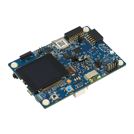
STM32L562E-DK, shown in
Figure
1, associated with the fan-out expansion board, is used as a reference design for user
application development, although it is not considered as the final application.
The full range of hardware features on the board helps the user to evaluate all the peripherals (USB, USART, digital
™
microphones, ADC and DAC, TFT LCD, Octo-SPI Flash memory device, microSD
card, audio codec, joystick, user button,
®
Bluetooth
Low Energy, accelerometer and gyroscope) and to develop applications. Extension headers allow easy connection
of a daughterboard or wrapping board for a specific application.
An STLINK-V3E is integrated on the board, as embedded in-circuit debugger and programmer for the STM32 MCU and the
USB Virtual COM port bridge.
Figure 1.
STM32L562E-DK Discovery kit (top view)
Picture is not contractual.
UM2617 - Rev 2 - January 2020
www.st.com
For further information contact your local STMicroelectronics sales office.
Advertisement
Table of Contents

Related Manuals for ST STM32L562E-DK


Summary of Contents for ST STM32L562E-DK
-
Page 1: Figure 1. Stm32L562E-Dk Discovery Kit (Top View)
UM2617 User manual Discovery kit with STM32L562QE MCU Introduction The STM32L562E-DK Discovery kit is designed as a complete demonstration and development platform for STMicroelectronics ® ® ® Cortex -M33 core-based STM32L562QEI6QU microcontroller with TrustZone . It features 256 Kbytes of internal SRAM and 512 Kbytes of internal Flash memory, one flexible memory controller (FMC) interface, one Octo-SPI memory interface, one ™... -
Page 2: Features
Audio MEMS daughterboard expansion connector ® – ARDUINO Uno V3 expansion connector • Flexible power-supply options: ST-LINK, USB V or external sources • On-board STLINK-V3E debugger/programmer with USB re-enumeration capability: mass storage, Virtual COM port, and debug port • Comprehensive free software libraries and examples available with the... -
Page 3: Ordering Information
Evaluation tools marked as “ES” or “E” are not yet qualified and therefore not ready to be used as reference design or in production. Any consequences deriving from such usage will not be at ST charge. In no event, ST will be liable for any customer usage of these engineering sample tools as reference designs or in production. -
Page 4: Development Environment
STM32 Flash memory for easy demonstration of the device peripherals in standalone mode. The latest versions of the demonstration source code and associated documentation can be downloaded from www.st.com. UM2617 - Rev 2 page 4/61... -
Page 5: Conventions
UM2617 Conventions Conventions Table 3 provides the conventions used for the ON and OFF settings in the present document. Table 3. ON/OFF convention Convention Definition Jumper JPx ON Jumper fitted Jumper JPx OFF Jumper not fitted Jumper JPx [1-2] Jumper should be fitted between Pin 1 and Pin 2 Solder bridge SBx ON SBx connections closed by 0 Ω... -
Page 6: Delivery Recommendations
UM2617 Delivery recommendations Delivery recommendations Before the first use, make sure that no damage occurred to the board during shipment and no socketed components are not firmly fixed in their sockets or loose in the plastic bag. UM2617 - Rev 2 page 6/61... -
Page 7: Hardware Layout And Configuration
UM2617 Hardware layout and configuration Hardware layout and configuration The STM32L562E-DK Discovery kit is designed around the STM32L562QEI6QU target microcontroller. Figure 2 illustrates STM32L562QEI6QU connections with peripheral components. Figure 3 shows the location of the main components on the top side of the Discovery board and... -
Page 8: Figure 3. Stm32L562E-Dk Pcb Layout (Top View)
UM2617 Hardware layout and configuration Figure 3. STM32L562E-DK PCB layout (top view) Figure 4. STM32L562E-DK PCB layout (bottom view) UM2617 - Rev 2 page 8/61... -
Page 9: Embedded Stlink-V3E
USB_DEV_HS_CN_P PB15 6.1.2 Drivers Before connecting the STM32L562E-DK board to a Windows PC via USB, the user must install a driver for the STLINK-V3E (not required for Windows 10). It is available on the www.st.com website. In case the STM32L562E-DK board is connected to the PC before the driver is installed, some STM32L562E-DK interfaces may be declared as “Unknown”... -
Page 10: Stlink-V3E Firmware Upgrade
STM32L562E-DK Discovery kit and periodically, to stay up-to-date with the latest firmware version. 6.1.4 Using an external debug tool to program and debug the onboard STM32 There are 2 basic ways to support an external debug tool: Keep the embedded STLINK-V3E running. -
Page 11: Table 5. Stdc14 Connector Pinout
UM2617 Embedded STLINK-V3E Figure 7 shows the CN8 STDC14 connector pinout. Figure 7. CN8 STDC14 connector pinout Table 5 describes the CN8 STDC14/MIPI10 debug connector pinout. Table 5. STDC14 connector pinout STM32 pin Board function Board function STM32 pin T.SWDIO: Target SWDIO using SWD protocol or Target Power PA13... -
Page 12: Tag Footprint
UM2617 TAG footprint TAG footprint The CN9 TAG footprint can also output a debug interface compatible with the TAG probe TC2050-IDC-NL. Figure 8 shows the TAG connector pinout. Figure 8. CN9 TAG connector pinout Table 6 describes the CN9 TAG connector pinout. Table 6. -
Page 13: Power Supply
CN18 pin 5, or directly after the JP4 connector for 5 V selection When 5V_VIN, 5V_CHG, 5V_DC or 3V3 is used to power the STM32L562E-DK board, this power source must comply with the standard EN-60950-1: 2006+A11/2009 and must be Safety Extra Low Voltage (SELV) with limited power capability LD12 Green LED turns on when the voltage on the power line marked as 5 V is present. -
Page 14: 5V_Vin Power Source: 7 To 12 V, 800 Ma Maximum
UM2617 Power supply 6.3.2 Power supply input from STLINK-V3E USB connector (default setting): 5V/500mA 5V_STLK is a DC power with limitation from CN17 STLINK-V3E USB connector, the USB type Micro-B connector of STLINK-V3E. In this case, the JP4 jumper must be on pin [1-2] to select 5V_STLK power source on JP4 silkscreen. -
Page 15: 5V_Ucpd Power Source: 5 V, 1 A Maximum
UM2617 Power supply Figure 10. JP4 [3-4]: 5V_VIN PWR SOURCE 6.3.4 5V_UCPD power source: 5 V, 1 A maximum ™ 5V_UCPD is the DC power supply connected to the CN15 user USB Type-C connector for Power Delivery. To select the 5V_UCPD power source on the JP4 silkscreen, the JP4 jumper must be on pins [5-6]. 5V_UCPD power source configuration for jumper JP4 [5-6] is described in Figure 11 Figure 11. -
Page 16: 5V_Pm Power Source: 5 V, 500 Ma
5V_CHG is the DC power charger connected to CN17 USB STLINK-V3E. To select the 5V_CHG power source on JP4 silkscreen, the JP4 jumper must be on pins [9-10]. In this case, if the STM32L562E-DK board is powered by an external USB charger, then the debug on the STLINK-V3E USB connector is not available. -
Page 17: 5V_Dc Power Source
UM2617 Power supply Figure 13. JP4 [9-10]: CN17 5V_CHG PWR SOURCE Note: With this JP4 configuration: 5V_CHG, the USB_PWR protection is bypassed. Never use this configuration with a computer connected instead of the charger, because as the USB_PWR_protection is bypassed, and if the board consumption is more than 500mA, this can damage the computer. -
Page 18: Programing/Debugging When The Power Supply Is Not From Stlink-V3E (5V_Stlk)
Regardless of the 5V power source, a U46 DC-DC converter is used to deliver a fixed 3.3 V power supply, with a current capability of 300 mA. This power source of 3.3 V is shared between the STM32L562E-DK and its expansion board. -
Page 19: Table 8. Vdd_Mcu Power Selection
JP3 [x-x] SW1 [2-3] [6-7] Current measurement selection VDD_MCU and to perform current consumption measurement. 1. The default configuration is shown in bold. Figure 16 describes the VDD_MCU power selection on the STM32L562E-DK board. UM2617 - Rev 2 page 19/61... -
Page 20: Rss/Bootloader
VDD_MCU power selection RSS/bootloader The bootloader is located in the system memory, programmed by ST during production. It is used to reprogram the Flash memory by using USART, I C, SPI, CAN FD or USB FS in device mode through the DFU (device firmware upgrade). -
Page 21: Boot From Rss
Boot from RSS On STM32L562E-DK, the PH3-BOOT0 is fixed to a LOW level allowing the boot from the memory address defined by SECBOOTADD0 option byte. In order to change the boot from RSS, it is needed to set the PH3- BOOT0 to the HIGH level by removing R32 and soldering R31, or just by applying 3V3 on PH3-BOOT0 signal between R32 and R31. -
Page 22: Reset Source
PH1 not used as GPIO 1. The default configuration is shown in bold. Reset source The reset signal of the STM32L562E-DK Discovery kit is active low. Internal PU force the RST signal to a high level. Sources of reset are: •... -
Page 23: Operating Voltage
UM2617 Audio There is one low-power digital microphone on-board of the STM32L562E-DK. The Discovery kit offers the possibility to connect a MEMS expansion module. 6.7.2 Operating voltage The microphone is supplied by VDD and is compatible with the VDD_MCU voltage range from 1.8 to 3.3 V. The audio codec has two supplies: •... -
Page 24: Digital Microphone Interface
OUT_SPEAKER_RIGHT 6.7.6 Digital microphone interface A low power digital microphone U16 is available on STM32L562E-DK. The interface used for this microphone is the DFSDM1 with DFSDM1_CKOUT and DFSDM1_DATIN1. The microphone is supplied with a programmable clock directly generated by STM32L562QEI6QU. -
Page 25: I/O Restriction To Other Features
When a USB host connection to the CN15 USB Type-C connector of STM32L562E-DK is detected, the STM32L562E-DK Discovery kit starts behaving as a USB device. Depending on the powering capability of the USB host, the board can take power from the V terminal of CN15. -
Page 26: Usb Type-C™ Connector
UCPD_FLT: This signal is provided by the STM Type-C port Protection. It is used as fault reporting to MCU after a bad V level detection. By design, R45 set to 2.7 kΩ, the STM32L562E-DK protection is set to 6 V maximum. -
Page 27: I/O Restriction To Other Features
UM2617 microSD™ card STM32 pin Signal name Signal name STM32 pin VBUSc VBUSc PA15 SBU2 PA12 PA11 PA11 PA12 SBU1 PB15 VBUSc VBUSc RX2- TX2- RX2+ TX2+ 6.8.6 I/O restriction to other features Caution: Due to the sharing of some I/Os of STM32L562QEI6QU by multiple peripherals, the following limitations apply in using the USB features: The USB UCPD cannot be operated simultaneously with full JTAG (JTDI). -
Page 28: Table 19. Cn1 Sd Card Connector Pinout
UM2617 microSD™ card Configuration PC11 is connected to SDCARD SDIO_D3. PC11 ™ PC11 is shared with Pmod pin3 / STMod+ pin 3 (UART_RX function). PC12 PC12 is connected to SDCARD SDIO_CLK. PD2 is connected to SDCARD SDIO_CMD. ™ PD2 is shared with Pmod pin 4 / STMod+ pin 3 (UART_RTS function). -
Page 29: I/O Restriction To Other Features
PD3 is connected to the red LED LD9 and active low. 6.11 Physical input devices: buttons 6.11.1 Description The STM32L562E-DK Discovery kit provides two push buttons for physical human control. • The USER button (B2), • The RST reset button (B1). -
Page 30: Octo-Spi Memory Devices
Octo-SPI memory devices 6.12.1 Description MX25LM51245GXDI00, a 512-Mbit Octal-SPI Flash memory device, is fitted on STM32L562E-DK, in the U6 position. It is used when evaluating the STM32L562QEI6QU Octo-SPI interface. MX25LM51245GXDI00 can operate in both single (STR) and double (DTR) transfer-rate modes. -
Page 31: 3D-Accelerometer And 3D-Gyroscope
PB0 is connected to SPI1.SCK. 6.14 3D-accelerometer and 3D-gyroscope 6.14.1 Description The STM32L562E-DK Discovery kit supports a 3d accelerometer and a 3d gyroscope. These functions are supported by the STM module LSM6DSO. This module is driven by an I C interface. 6.14.2 Operating voltage The LSM6DSO module supports the voltage range from 1.8 to 3.3 V. - Page 32 UM2617 TFT LCD Configuration PD5 is used as LCD.FMC_NWE. PD4 is used as LCD.FMC_NOE. PF0 is used as LCD.FMC_A0_RS. PD14 PD14 is used as LCD.FMC_D0. PD15 PD15 is used as LCD.FMC_D1. PD0 is used as LCD.FMC_D2. PD1 is used as LCD.FMC_D3. PE7 is used as LCD.FMC_D4.
-
Page 33: Table 26. Cn7 Lcd Connector Pinout
UM2617 TFT LCD Figure 21. CN7 LCD connector pinout Table 26 describes the CN7 LCD interface and connector pinout. Table 26. CN7 LCD connector pinout STM32 STM32 Function Signal name Pin name Pin name Signal name Function FMARK LCD.TE LCD.TE PD10 LCD.FMC_D15 DB15... -
Page 34: Pmod™ Connector
6.16 Pmod™ connector 6.16.1 Description ™ The CN4 Pmod standard connector is in the STM32L562E-DK board to support flexibility in small form factor ™ ™ application. The Pmod connector implements the Pmod type 2A and 4A on the STM32L562E-DK board. -
Page 35: Table 28. I/O Configuration For The Pmod™ Interface
UM2617 Pmod™ connector Table 28. I/O configuration for the Pmod™ interface I/O PF12 I/O PF11 STMod+ STMod+ Configuration SEL_34 SEL_12 SPI interface PB13/PB5/PB4/PG9 used for SPI mode mikroBUS™ interface PC10/PC11 for UART mode and PB13/PG9 for SPI mode Not used UART interface PB13/PC10/PC11/PD2 used for UART mode 1. -
Page 36: I/O Restriction To Other Features
6.17 STMod+ connector 6.17.1 Description The CN3 STMod+ standard connector is on the STM32L562E-DK board to support flexibility in small form factor ® application. The STMod+ expansion connector supports the fan-out expansion board (MB1280) for Wi‑Fi , Grove and mikroBUS™ compatible connectors 6.17.2... -
Page 37: I/O Restriction To Other Features
UM2617 STMod+ connector Figure 24. CN3 STMod+ connector pinout Table 31 describes the CN3 STMod+ interface and connector pinout. Table 31. CN3 STMod+ interface and connector pinout STM32 STM32 MCU Function Function Function MCU Function SPI3 PB13 SPI_NSS PMOD_INT INT5 USART3 PB13 UART_CTS... -
Page 38: Arduino® Connectors
The ARDUINO Uno V3 connector supports 5 V, 3.3 V and VDD for I/O compatibility. VIN, voltage range from 7 to ® 12 V is also available to supply the STM32L562E-DK Discovery kit from an ARDUINO shield. Section 6.3 Power supply provides information on how to use the powering option. -
Page 39: Table 32. I/O Configuration For The Arduino ® Interface
UM2617 ARDUINO® connectors ® Table 32. I/O configuration for the ARDUINO interface Configuration PA0 is used as ARD.A0: ADC1_IN5. shared with STMod+. PA1 is used as ARD.A1: ADC1_IN6. R33 OFF PA4 is used as ARD.A2: ADC1_IN9 only. PA4 is used as ARD.A2: ADC1_IN9. R33 ON Shared with USB_C.VBUS_SENSE PA5 is used as ARD.A3: ADC1_IN10. -
Page 40: Table 33. Arduino ® Connector Pinout
UM2617 ARDUINO® connectors ® Table 33. ARDUINO connector pinout Connector Pin names Function STM32 pin MCU Function NC (reserved for the test) IOREF (VDD 1V8 or 3V3) NRST NRST NRST CN18 VIN 7V-12V ARD_ADC.A0 ADC1_IN5 ARD_ADC.A1 ADC1_IN6 ARD_ADC.A2 ADC1_IN9 CN19 ARD_ADC.A3 ADC1_IN10 ARD_ADC.A4... -
Page 41: Mcu Energy Meter Tools
This function is performed with the support of the U22 STM32L496VGT6 MCU. The energy meter tools included on the STM32L562E-DK are a part of the standalone board X-NUCLEO-LPM01A, also called PowerShield. The X-NUCLEO-LPM01A expansion board is a programmable power supply source, from 1.8 to 3.3 V, with advanced power consumption measurement capability. -
Page 42: Figure 27. Energy Metering Firmware Update Hardware
Energy meter firmware update The Energy meter firmware can be upgraded with the following procedure: Get the PowerShield firmware binary file on www.st.com: firmware binary file has the extension “.dfu” standing for Device Firmware Upgrade (DFU). Download and install USB-DFU driver and utility: software reference: STSW-STM320803. -
Page 43: Fan-Out Board (Mb1280)
Fan-out board (MB1280) The fan-out board, shown in Figure 29, is included in the STM32L562E-DK Discovery kit. It can be connected to STMod+ connector (CN3) and it provides access to: • MikroElektronika Click board compatible connectors (MB1280 CN10 and CN11: two 1x8-pin female connectors) •... -
Page 44: Mikroelektronika Mikrobus™ Compatible Connector (Fan-Out Cn10 / Cn11)
UM2617 Fan-out board (MB1280) Figure 29. STMod+ fan-out board plugged into CN1 connector 6.20.1 MikroElektronika mikroBUS™ compatible connector (Fan-out CN10 / CN11) The mikroBUS™ compatible connector is 2.54" pitch with a pair of 1x8-pin female connectors. Table 34 shows the assignment of CN10 and CN11 mikroBUS™... -
Page 45: Compatible Connectors For The Grove Boards
UM2617 Fan-out board (MB1280) 6.20.3 Compatible connectors for the Grove boards The two connectors of the Grove board are 2.54"-pitch with 1x4-pin male connectors. The part number is 1125S- SMT-4P. Warning: On MB1280 PCBs revision A and B, the I C interface is only 3.3 V tolerant. -
Page 46: Limitation
UM2617 Limitation Limitation RSS and bootloader limitation Issue observed: The STM32L5 part soldered on STM32L562E-DK that embeds the bootloader V9.0 is affected by the limitations described in Section 6.4.1 RSS limitation. Proposed workaround: Refer to Section 6.4.1 RSS limitation to detail workaround. -
Page 47: Appendix Astm32L562E-Dk Jumper Summary
Appendix A STM32L562E-DK jumper summary Figure 30 Figure 31 summarize the default setting of the STM32L562E-DK jumpers and switches. Figure 30. Default jumper and switch setting of the STM32L562E-DK (top view) Figure 31. Default jumper and switch setting of the STM32L562E-DK (bottom view) -
Page 48: Appendix Bstm32L562E-Dk I/O Assignment
UM2617 STM32L562E-DK I/O assignment Appendix B STM32L562E-DK I/O assignment Table 38. STM32L562E-DK I/O assignment Main function Optional function Pin name pinout pinout assignment pinout assignment SAI.SCK_A SAI.SD_B LCD.BL_CTRL ARD.D9_TIM I2C1_SCL PG12 LED_GREEN STMod+ 8_SPI_MOSIs LCD.FMC_NWE SDIO.CMD STMod+ 4_UART_RTS PC11 SDIO.D3... - Page 49 UM2617 STM32L562E-DK I/O assignment Main function Optional function Pin name pinout pinout assignment pinout assignment PC15 OSC32_OUT LCD.FMC_A0_RS GYRO_ACC_INT POWER / VDD_MCU I2C1_SDA USB_C.DBn STMod+ 2_SPI_MOSIp ARD.D11_TIM_SPI_MOSI LCD.FMC_NE1_CS VDDIO POWER / VDDIO2 POWER / VDD_MCU T.VCP_TX ARD.D1_TX PA10 T.VCP_RX ARD.D0_RX LCD.TE...
- Page 50 UM2617 STM32L562E-DK I/O assignment Main function Optional function Pin name pinout pinout assignment pinout assignment SPI1.BLE_CS VSSA POWER / GND OCTOSPI.IO7 OPAM1_VINM POWER / GND POWER / GND PD14 LCD.FMC_D0 PD13 ARD.D5_TIM PD15 LCD.FMC_D1 VREFP POWER / VREFP ARD_ADC.A0 STMod+ 13_ADC ARD_ADC.A5...
- Page 51 UM2617 STM32L562E-DK I/O assignment Main function Optional function Pin name pinout pinout assignment pinout assignment PE11 LCD.FMC_D8 PE15 LCD.FMC_D12 PB11 ARC.D1_TX T.VCP_TX VSS_SMPS POWER / GND PB12 DFSDM_DATIN1 LCD.FMC_D13 ARD_ADC.A3 OPAM2_VINM ARD_ADC.A4 OCTOSPI.IO1 PF13 ARD.D8_IO LCD.FMC_D6 PE13 LCD.FMC_D10 VDD_SMPS POWER / VDDSMPS...
-
Page 52: Appendix C Federal Communications Commission (Fcc) And Industry Canada (Ic)
UM2617 Federal Communications Commission (FCC) and Industry Canada (IC) Compliance Statements Appendix C Federal Communications Commission (FCC) and Industry Canada (IC) Compliance Statements FCC Compliance Statement Part 15.19 This device complies with Part 15 of the FCC Rules. Operation is subject to the following two conditions: (1) this device may not cause harmful interference, and (2) this device must accept any interference received, including interference that may cause undesired operation. -
Page 53: Warning
UM2617 Warning Warning EN 55032 / CISPR32 (2012) Class A product Warning: this device is compliant with Class A of EN55032 / CISPR32. In a residential environment, this equipment may cause radio interference. Avertissement : cet équipement est conforme à la Classe A de la EN55032 / CISPR 32. Dans un environnement résidentiel, cet équipement peut créer des interférences radio. -
Page 54: Revision History
UM2617 Revision history Table 39. Document revision history Date Revision Changes 29-Nov-2019 Initial release. Added: • Section 7 Limitation 28-Jan-2020 Updated: • Section 6.4 RSS/bootloader UM2617 - Rev 2 page 54/61... -
Page 55: Table Of Contents
UM2617 Contents Contents Features................2 Ordering information . - Page 56 UM2617 Contents 6.4.2 Boot from RSS ............21 Clock source .
- Page 57 UM2617 Contents 6.11.3 Physical input I/O interface ..........29 6.12 Octo-SPI memory devices .
- Page 58 STM32L562E-DK jumper summary ........
-
Page 59: List Of Tables
STM32L562E-DK I/O assignment ........ -
Page 60: List Of Figures
Default jumper and switch setting of the STM32L562E-DK (top view) ......47... - Page 61 ST’s terms and conditions of sale in place at the time of order acknowledgement. Purchasers are solely responsible for the choice, selection, and use of ST products and ST assumes no liability for application assistance or the design of Purchasers’...
Need help?
Do you have a question about the STM32L562E-DK and is the answer not in the manual?
Questions and answers