Sign In
Upload
Manuals
Brands
ST Manuals
Microcontrollers
STM32L562E-DK
ST STM32L562E-DK Manuals
Manuals and User Guides for ST STM32L562E-DK. We have
2
ST STM32L562E-DK manuals available for free PDF download: User Manual
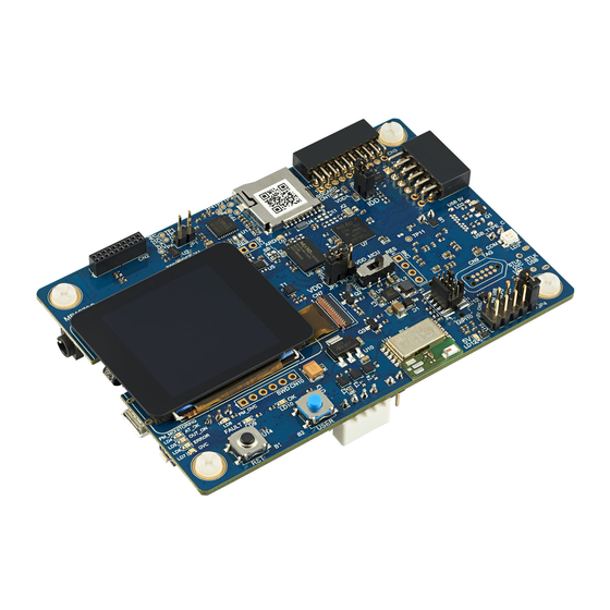
ST STM32L562E-DK User Manual (61 pages)
Discovery kit with STM32L562QE MCU
Brand:
ST
| Category:
Microcontrollers
| Size: 7 MB
Table of Contents
Figure 1. STM32L562E-DK Discovery Kit (Top View)
1
1 Features
2
Table 1. Ordering Information
3
Table 2. Codification Explanation
3
2 Ordering Information
3
Product Marking
3
Codification
3
3 Development Environment
4
System Requirements
4
Development Toolchains
4
Demonstration Software
4
Table 3. ON/OFF Convention
5
4 Conventions
5
5 Delivery Recommendations
6
Figure 2. Hardware Block Diagram
7
6 Hardware Layout and Configuration
7
Figure 4. STM32L562E-DK PCB Layout (Bottom View)
8
Figure 3. STM32L562E-DK PCB Layout (Top View)
8
Embedded STLINK-V3E
9
Description
9
Drivers
9
Table 4. CN17 USB Micro-B Connector Pinout
9
Figure 7. CN8 STDC14 Connector Pinout
11
Table 5. STDC14 Connector Pinout
11
Figure 8. CN9 TAG Connector Pinout
12
Figure 9. JP4 [1-2]: 5V_STLK PWR SOURCE
14
5V_UCPD Power Source: 5 V, 1 a Maximum
15
Figure 10. JP4 [3-4]: 5V_VIN PWR SOURCE
15
Figure 11. JP4 [5-6]: CN15 5V_USB_TYPE_C PWR SOURCE
15
5V_CHG Power Source: 5 V
16
5V_PM Power Source: 5 V, 500 Ma
16
Figure 12. JP4 [7-8]: CN16 5V_PM PWR SOURCE
16
5V_DC Power Source
17
Figure 13. JP4 [9-10]: CN17 5V_CHG PWR SOURCE
17
Figure 14. JP4 [-]: 5V_DC PWR SOURCE
17
External Power Supply Output
18
Internal Power Supply
18
Programing/Debugging When the Power Supply Is Not from STLINK-V3E (5V_STLK)
18
Figure 15. VDD_MCU Power Selection Schematics
19
Table 8. VDD_MCU Power Selection
19
Figure 16. VDD_MCU Power Selection
20
RSS Limitation
20
Rss/Bootloader
20
Boot from RSS
21
Clock Source
21
Figure 17. BOOT0 Modification to Set the HIGH Level
21
HSE Clock Reference
21
LSE Clock Reference
21
Audio
22
Description
22
Reset Source
22
Table 9. I/O Configuration for the Optional HSE
22
Audio Codec Interface
23
Audio Jack Connector
23
Figure 18. CN13 Audio Jack Connector
23
Headphones Outputs
23
Operating Voltage
23
Table 10. I/O Configuration for the Audio Interface
23
Digital Microphone Interface
24
Table 11. CN13 Audio Jack Connector Pinout
24
Table 12. I/O Configuration for the U13 AUDIO MEMS
24
Table 13. CN13 Audio Jack Connector Pinout
24
Description
25
I/O Restriction to Other Features
25
Operating Voltage
25
Ucpd
25
USB FS Device
25
USB Type-C™ FS Port
25
Table 6. CN9 TAG Connector Pinout
12
TAG Footprint
12
Power Supply
13
5 V Power Supply General View
13
Power Supply Input from STLINK-V3E USB Connector (Default Setting): 5V/500Ma
13
5V_VIN Power Source: 7 to 12 V, 800 Ma Maximum
14
Figure 5. USB Composite Device
10
Figure 6. Connecting an External Debug Tool to Program the On-Board STM32L5
10
STLINK-V3E Firmware Upgrade
10
Using an External Debug Tool to Program and Debug the Onboard STM32
10
Table 15. I/O Configuration for the USB Interface
25
Table 14. I/O Configuration for the Audio DFSDM Interface
25
Figure 19. CN15 USB Type-C ™ Connector Pinout
26
Figure 20. CN1 SD Card Connector
28
Description
29
LED Interface
29
Operating Voltage
29
Table 20. HW Configuration for the LED Interface
29
Table 21. I/O Configuration for the Physical User Interface
29
User Leds
29
BLE I/O Interface
30
Bluetooth ® Low Energy (BLE)
30
Description
30
Octo-SPI I/O Interface
30
Octo-SPI Memory Devices
30
Operating Voltage
30
Table 22. I/O Configuration for the Octo-SPI Interface
30
Table 23. I/O Configuration for the BLE I/O Interface
30
3D Accelerator and Gyrometer Interface
31
3D-Accelerometer and 3D-Gyroscope
31
Description
31
LCD Interface
31
Operating Voltage
31
Table 24. I/O Configuration for the 3D ACC/GYRO Interface
31
Table 25. I/O Configuration for the LCD and CTP Interface
31
Tft Lcd
31
Figure 21. CN7 LCD Connector Pinout
33
Table 26. CN7 LCD Connector Pinout
33
Description
34
Operating Voltage
34
Pmod™ Connector
34
Pmod™ Interface
34
Table 18. I/O Configuration for the SDIO Interface
27
Table 19. CN1 SD Card Connector Pinout
28
I/O Restriction to Other Features
29
Physical Input Devices: Buttons
29
Physical Input I/O Interface
29
Table 17. CN15 USB Type-C ™ Connector Pinout
26
Table 16. I/O Configuration for the UCPD Feature
26
USB Type-C™ Connector
26
I/O Restriction to Other Features
27
Microsd™ Card
27
Description
27
Operating Voltage
27
SD Card Interface
27
Table 27. CN14 Touch Panel Connector Pinout
34
Figure 23. CN4 Pmod ™ Connector Pinout
35
Table 28. I/O Configuration for the Pmod™ Interface
35
Table 29. CN4 Pmod ™ Connector Pinout
35
Table 30. I/O Configuration for the Stmod+ Interface
36
Figure 24. CN3 Stmod+ Connector Pinout
37
Table 31. CN3 Stmod+ Interface and Connector Pinout
37
ARDUINO ® Interface
38
ARDUINO® Connectors
38
Description
38
Operating Voltage
38
I/O Restriction to Other Features
37
Figure 25. ARDUINO ® Connector Pinouts
38
Table 32. I/O Configuration for the ARDUINO ® Interface
39
Figure 26. Energy Metering Hardware Configuration
41
Figure 27. Energy Metering Firmware Update Hardware
42
Fan-Out Board (MB1280)
43
Figure 28. Energy Metering Firmware Upgrade Software
43
ESP-01 Wi-Fi
44
Figure 29. Stmod+ Fan-Out Board Plugged into CN1 Connector
44
Mikroelektronika Mikrobus™ Compatible Connector (Fan-Out CN10 / CN11)
44
Compatible Connectors for the Grove Boards
45
Table 33. ARDUINO ® Connector Pinout
40
MCU Energy Meter Tools
41
Description
41
Energy Meter Firmware Update
41
IDD Measurement
41
Operating Voltage
41
Figure 22. CN14 LCD Touch Panel Connector Pinout
34
I/O Restriction to Other Features
36
Stmod+ Connector
36
Description
36
Operating Voltage
36
Stmod+ Interface
36
Table 34. Description of the Mikrobus™ Connector Pins
44
Table 35. Description of the ESP-01 Wi-Fi ® Connector Pins
44
Table 36. Description of the I C Grove Board CN3 Connector Pins
45
Table 37. Description of the UART Grove Board CN2 Connector Pins
45
7 Limitation
46
RSS and Bootloader Limitation
46
SMPS Limitation
46
Appendix Astm32L562E-Dk Jumper Summary
47
Figure 30. Default Jumper and Switch Setting of the STM32L562E-DK (Top View)
47
Figure 31. Default Jumper and Switch Setting of the STM32L562E-DK (Bottom View)
47
Appendix Bstm32L562E-Dk I/O Assignment
48
Table 38. STM32L562E-DK I/O Assignment
48
Appendix C Federal Communications Commission (FCC) and Industry Canada (IC)
52
Compliance Statements
52
FCC Compliance Statement
52
IC Compliance Statement
52
Warning
53
Revision History
54
Table 39. Document Revision History
54
Table of Contents
55
Contents
55
List of Tables
59
List of Figures
60
Advertisement
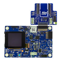
ST STM32L562E-DK User Manual (64 pages)
Discovery kit with STM32L562QE MCU
Brand:
ST
| Category:
Computer Hardware
| Size: 4 MB
Table of Contents
Figure 1. STM32L562E-DK Discovery Kit (Top View)
1
Features
2
Ordering Information
3
Codification
3
Table 1. Ordering Information
3
Table 2. Codification Explanation
3
Development Environment
4
System Requirements
4
Development Toolchains
4
Demonstration Software
4
Conventions
5
Table 3. ON/OFF Convention
5
Delivery Recommendations
6
Hardware Layout and Configuration
7
Figure 2. Hardware Block Diagram
7
Figure 3. STM32L562E-DK PCB Layout (Top View)
8
Figure 4. STM32L562E-DK PCB Layout (Bottom View)
8
Embedded STLINK-V3E
9
Description
9
Drivers
9
Table 4. USB Micro-B Connector (CN17) Pinout
9
STLINK-V3E Firmware Upgrade
10
Using an External Debug Tool to Program and Debug the Onboard STM32
10
Figure 5. USB Composite Device
10
Figure 6. Connecting an External Debug Tool to Program the On-Board STM32L5
10
Table 5. STDC14 Connector Pinout
11
Figure 7. STDC14 Connector (CN8) Pinout
11
TAG Footprint
12
Table 6. TAG Connector (CN9) Pinout
12
Figure 8. TAG Connector (CN9) Pinout
12
Power Supply
13
5 V Power Supply General View
13
Table 7. Power Supply Capabilities
13
Power Supply Input from an STLINK-V3E USB Connector (Default Setting): 5 V/500 Ma
14
Figure 9. JP4 [1-2]: 5V_STLK PWR SOURCE
14
5V_VIN Power Source: 7 to 12 V, 800 Ma Maximum
15
5V_UCPD Power Source: 5 V, 1 a Maximum
15
Figure 10. JP4 [3-4]: 5V_VIN PWR SOURCE
15
Figure 11. JP4 [5-6]: 5V_USB_TYPE_C PWR SOURCE (CN15)
15
5V_PM Power Source: 5 V, 500 Ma
16
5V_CHG Power Source: 5 V
16
Figure 12. JP4 [7-8]: 5V_PM PWR SOURCE (CN16)
16
Figure 13. JP4 [9-10]: 5V_CHG PWR SOURCE (CN17)
16
5V_DC Power Source
17
Figure 14. JP4 [-]: 5V_DC PWR SOURCE
17
Programing/Debugging When the Power Supply Is Not from STLINK-V3E (5V_STLK)
18
External Power Supply Output
18
Internal Power Supply
18
Table 8. VDD_MCU Power Selection
19
Figure 15. VDD_MCU Power Selection Schematics
19
Rss/Bootloader
20
Limitation
20
Figure 16. VDD_MCU Power Selection
20
Boot from RSS
21
Figure 17. BOOT0 Modification to Set the High-Level Logic
21
Clock Source
22
LSE Clock Reference
22
HSE Clock Reference
22
Reset Source
22
Table 9. I/O Configuration for the Optional HSE
22
Audio
23
Description
23
Operating Voltage
23
Audio Codec Interface
23
Headphones Outputs
23
Table 10. I/O Configuration for the Audio Interface
23
Audio Jack Connector
24
Digital Microphone Interface
24
Table 11. Audio Jack Connector (CN13) Pinout
24
Table 12. I/O Configuration for the U13 AUDIO MEMS
24
Figure 18. Audio Jack Connector (CN13)
24
I/O Restriction to Other Features
25
Table 13. Audio Jack Connector (CN13) Pinout
25
Table 14. I/O Configuration for the Audio DFSDM Interface
25
USB Type-C ® FS Port
26
Description
26
Operating Voltage
26
USB FS Device
26
Ucpd
26
Table 15. I/O Configuration for the USB Interface
26
USB Type-C Connector
27
Table 16. I/O Configuration for the UCPD Feature
27
Table 17. USB Type-C ® (CN15) Connector Pinout
27
Figure 19. USB Type-C ® Connector (CN15) Pinout
27
I/O Restriction to Other Features
28
Microsd™ Card
28
Description
28
Operating Voltage
28
SD Card Interface
28
Table 18. I/O Configuration for the SDIO Interface
28
I/O Restriction to Other Features
29
Table 19. SD Card Connector (CN1) Pinout
29
Figure 20. SD Card Connector (CN1)
29
User Leds
30
Description
30
Operating Voltage
30
LED Interface
30
Physical Input Devices: Buttons
30
Physical Input I/O Interface
30
Table 20. Hardware Configuration for the LED Interface
30
Table 21. I/O Configuration for the Physical User Interface
30
Octo-SPI Memory Devices
31
Description
31
Operating Voltage
31
Octo-SPI I/O Interface
31
Table 22. I/O Configuration for the Octo-SPI Interface
31
Bluetooth ® Low Energy
32
Description
32
Operating Voltage
32
Bluetooth ® Low Energy I/O Interface
32
3D Accelerometer and 3D Gyroscope
32
3D Accelerator and 3D Gyrometer Interface
32
Table 23. I/O Configuration for the Bluetooth ® Low Energy I/O Interface
32
Table 24. I/O Configuration for the 3D ACC/GYRO Interface
32
Tft Lcd
33
Description
33
Operating Voltage
33
LCD Interface
34
Table 25. I/O Configuration for the LCD and CTP Interface
34
Figure 21. LCD Connector (CN7) Pinout
35
Table 26. LCD Connector (CN7) Pinout
36
Figure 22. LCD Touch-Panel Connector (CN14) Pinout
36
Pmod™ Connector
37
Description
37
Operating Voltage
37
Pmod ™ Interface
37
Table 27. Touch-Panel Connector (CN14) Pinout
37
Table 28. I/O Configuration for the Pmod ™ Interface
37
I/O Restriction to Other Features
38
Table 29. Pmod ™ Connector (CN4) Pinout
38
Figure 23. Pmod ™ Connector (CN4) Pinout
38
Stmod+ Connector
39
Description
39
Operating Voltage
39
Stmod+ Interface
39
Table 30. I/O Configuration for the Stmod+ Interface
39
Figure 24. Stmod+ Connector (CN3) Pinout
39
I/O Restriction to Other Features
40
ARDUINO® Connectors
40
Description
40
Operating Voltage
40
Table 31. Stmod+ Interface and Connector (CN3) Pinout
40
ARDUINO ® Interface
41
Figure 25. ARDUINO ® Connector Pinouts
41
Table 32. I/O Configuration for the ARDUINO ® Interface
42
Table 33. ARDUINO ® Connector Pinout
43
MCU Energy Meter Tools
44
Description
44
Operating Voltage
44
IDD Measurement
44
Figure 26. Energy Metering Hardware Configuration
44
Energy Meter Firmware Update
45
Figure 27. Energy Metering Firmware Update Hardware
45
Figure 28. Energy Metering Firmware Upgrade Software
46
STM32L562E-DK Jumper Summary
47
Figure 29. Default Jumper and Switch Setting of the STM32L562E-DK (Top View)
47
Figure 30. Default Jumper and Switch Setting of the STM32L562E-DK (Bottom View)
47
STM32L562E-DK I/O Assignment
48
Table 34. STM32L562E-DK I/O Assignment
48
STM32L562E-DK Product Information
52
Product Marking
52
STM32L562E-DK Product History
53
Table 35. Product History
53
Board Revision History
54
Table 36. Board Revision History
54
Federal Communications Commission (FCC) and ISED Canada Compliance
55
Statements
55
FCC Compliance Statement
55
ISED-Canada User Manual Notice for Licence-Exempt Radio Apparatus
55
FCC and ISED-Canada RF Exposure Statements
55
CE Conformity
56
Table 37. Document Revision History
57
Advertisement
Related Products
ST STM32L5 Series
ST STM32L4R5 Series
ST STM32L4R7 Series
ST STM32L496QG
ST STM32L4A6VG
ST STM32L4A6ZG
ST STM32L4A6VGT6
ST STM32L486ZGT3
ST STM32L011 4 Series
ST STM32L021K4
ST Categories
Motherboard
Computer Hardware
Microcontrollers
Control Unit
Controller
More ST Manuals
Login
Sign In
OR
Sign in with Facebook
Sign in with Google
Upload manual
Upload from disk
Upload from URL