Table of Contents
Advertisement
Quick Links
Advertisement
Table of Contents

Related Manuals for Kontron MOPSlcdGX1


Summary of Contents for Kontron MOPSlcdGX1
- Page 1 MOPSlcdGX1 Product Manual Document Revision 1.3...
-
Page 3: Table Of Contents
MOPSlcdGX1 Product Manual Contents CONTENTS USER INFORMATION....................1 ....................1 BOUT ANUAL ....................1 OPYRIGHT OTICE ......................2 RADEMARKS ......................2 TANDARDS ......................2 ARRANTY ....................3 ECHNICAL UPPORT 2. INTRODUCTION ......................4 SPECIFICATIONS ......................5 ................5 UNCTIONAL PECIFICATIONS ................7 ECHANICAL PECIFICATIONS .................7 LECTRICAL PECIFICATIONS .................7 NVIRONMENTAL PECIFICATIONS 4. CPU, CHIPSET, AND SUPER I/O .................9 CPU........................9... - Page 4 MOPSlcdGX1 Product Manual Contents 10. KEYBOARD AND FRONT-PANEL INTERFACE ...........18 10.1 (X10) ....................18 ONNECTOR 10.2 ....................18 ONFIGURATION 10.3 ..................19 IGNAL ESCRPITIONS 10.4 ..................20 DAPTER ABLE INOUT 11. PS/2-MOUSE INTERFACE ..................21 11.1 (X20) ....................21 ONNECTOR 11.2 ....................21 ONFIGURATION 12. FLOPPY-DRIVE INTERFACE..................22 12.1...
- Page 5 MOPSlcdGX1 Product Manual Contents 20. APPENDIX A: SYSTEM-RESOURCE ALLOCATIONS.........38 20.1 I/O P ..................38 SSIGNMENTS 20.2 ..................38 NTERRUPT EQUEST INES 20.3 (DMA) C .............39 IRECT EMORY CCESS HANNELS 20.4 .................39 PPER EMORY 20.5 PCI D ......................39 EVICES 21. APPENDIX B: BIOS OPERATION................40 21.1...
-
Page 7: User Information
1.1.1 JUMPtec Brand JUMPtec Industrielle Computertechnik AG and Kontron Embedded Computers AG merged in July 2002. JUMPtec is now known as Kontron Embedded Modules GmbH. Products labeled and sold under the Kontron Embedded Modules name (formerly JUMPtec) are now considered Kontron products for all practical purposes, including warranty and support. -
Page 8: Trademarks
Within the warranty period, the repair of products is free of charge as long as warranty conditions are observed. You may receive a bill for test costs if Kontron Embedded Modules finds no fault with the product. You also may receive a bill for repairs if a product’s warranty has expired. -
Page 9: Technical Support
Web site for the latest product documentation, utilities, and drivers. If the information does not help solve the problem, contact us by email or telephone. The table below lists technical support contacts and service facilities for Kontron Embedded Modules. Asia... -
Page 10: Introduction
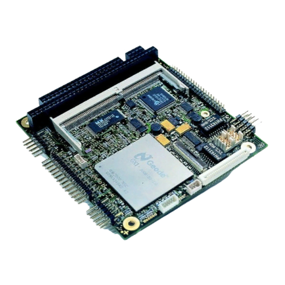
MOPSlcdGX1 Product Manual Introduction 2. INTRODUCTION The MOPSlcdGX1 provides a complete embedded solution and offers the latest in features and technology. The board uses the National GX1 CPU. PC/AT subsystems found in desktop units are built into the MOPSlcdGX1. Subsystems include: •... -
Page 11: Specifications
MOPSlcdGX1 Product Manual Specifications 3. SPECIFICATIONS Functional Specifications • National Semiconductor Geode GX1 Processor • Bus ♦ 200MHz (33Mhz bus clock) ♦ 266MHz (33Mhz bus clock) ♦ 300MHz (33Mhz bus clock) • Geode I/O Companion Multifunction South Bridge (CS5530A) chipset •... - Page 12 MOPSlcdGX1 Product Manual Specifications • Onboard CompactFlash socket ♦ Type 1 only for commercial compact flashes ♦ Master on secondary IDE ♦ Located on bottom of MOPSlcdGX1 board • USB ♦ Two USB-1.1 ports (OHCI) ♦ USB legacy-keyboard support • Two...
-
Page 13: Mechanical Specifications
MOPSlcdGX1 Product Manual Specifications Mechanical Specifications • Mechanical: 96mm x 90mm (3.8" x 3.6") • Mounting: Two pieces of 2x32 pin-male and 2x20 pin-male connector Electrical Specifications 3.3.1 Supply Voltage When operating a LCD panel, make sure you use a stable power supply, using the following volts. - Page 14 MOPSlcdGX1 Product Manual Specifications 3.4.2 Humidity • Operating: 10% to 90% (noncondensing) • Nonoperating: 5% to 95% (noncondensing) Kontron Embedded Modules Revision 1.3...
-
Page 15: Cpu, Chipset, And Super I/O
MOPSlcdGX1 Product Manual CPU, Chipset, and Super I/O 4. CPU, CHIPSET, AND SUPER I/O National Semiconductor Geode GX1 Processor features include: • Support for Intel’s MultiMedia eXtensions (MMX) instruction set extension for acceleration of multimedia applications • 16KB unified L1 cache •... -
Page 16: Super I/O
MOPSlcdGX1 Product Manual CPU, Chipset, and Super I/O • Boot-read only memory (ROM) and keyboard-chip select • Two controllers with support for up to three IDE devices • Independent timing for master and slave devices for both channels • PCI bus master burst reads and writes •... -
Page 17: System Memory
One socket is available for 3.3-volt (power level), unbuffered synchronous dynamic random access memory (SDRAM) of 8, 16, 32, 64, 128, or 256MB. To find the location of Connector X1 on the MOPSlcdGX1 board, please see the Appendix E: Connector Layout chapter. -
Page 18: Isa Expansion
8-bit, ISA-bus signals. X2a is a 40-pin connector of the same style and implements 16-bit expansion signals on the ISA bus. To find the location of Connectors X2a and X2b on the MOPSlcdGX1 board, please see Appendix E: Connector Layout chapter. -
Page 19: Configuration
PC/104 adapter cards are mounted in a stack-through manner. Adapter cards are designed with plugs on their undersides that mate with the PC/104 socket connectors of the MOPSlcdGX1. PC/104 adapters can support the socket-connector version on their topside and allow further stacking of adapters. -
Page 20: Usb Interface
For more information on USB interfaces, please see the Appendix G: Literature and Standards chapter. Connectors (X6 and X7) To find the location of Connectors X6 and X7 on the MOPSlcdGX1 board, please see the Appendix E: Connector Layout chapter. Pin Function USB- USB+ Use power contacts on Pin 1 and Pin 4 for internal USB devices only. -
Page 21: Serial-Communication Interface
Appendix G: Literature and Standards chapter. Connectors (X11 and X12) To find the location of Connectors X11 and X12 on the MOPSlcdGX1 board, please see Appendix E: Connector Layout chapter. COMA (X11) and COMB (X12) (RS232C) Signal Name In / Out... -
Page 22: Parallel-Communication Interface
For more information on parallel-communication interfaces, please see the Appendix G: Literature and Standards chapter. Connector (X15) To find the location of Connector X15 on the MOPSlcdGX1 board, please see the Appendix E: Connector Layout chapter. Parallel Port LPT 1 (X15) Signal Name... -
Page 23: Configuration
26-pin Header to 25-pin D-Subconversion Configuration The MOPSlcdGX1 parallel ports are bi-directional. The bi-directional functions are compatible with those of a PS/2 style parallel port. The functionality is always available and does not conflict with normal printer use. The parallel-port mode, I/O addresses, and IRQs are defined in the PhoenixBIOS Setup Utility. -
Page 24: Keyboard And Front-Panel Interface
For more information on keyboard and front-panel interfaces, please see the Appendix G: Literature and Standards chapter. 10.1 Connector (X10) To find the location of Connector X10 on the MOPSlcdGX1 board, please see the Appendix E: Connector Layout chapter. Signal Name Function... -
Page 25: Signal Descrpitions
MOPSlcdGX1 Product Manual Keyboard and Front-Panel Interface 10.3 Signal Descrpitions 10.3.1 KLOCK# (Keyboard Lock) • Input on CPU modules • Output on other modules • Input to keyboard controller: input port 1, bit 7 10.3.2 RESIN (Reset Input 1) • Input on CPU modules •... -
Page 26: Adapter Cable Pinout
10.3.6 VBAT (System Battery Connection) • This pin connects a system battery to all modules. • The battery voltage has to be higher than 2.85V and lower than 3.15V. Kontron Embedded Modules recommends a 3V battery (for example, CR2032). Note: There is no battery needed to hold CMOS-setup data. Your configuration information is saved in an onboard Ferroelectric Random-Access Memory (FRAM.) -
Page 27: Ps/2-Mouse Interface
MOPSlcdGX1 Product Manual PS/2-Mouse Interface 11. PS/2-MOUSE INTERFACE 11.1 Connector (X20) To find the location of Connector X20 on the MOPSlcdGX1 board, please see the Appendix E: Connector Layout chapter. Signal Name Function MSDAT PS/2 mouse data Power 5V Power ground... -
Page 28: Floppy-Drive Interface
For more information on floppy-drive interfaces, please see the Appendix G: Literature and Standards chapter. 12.1 Connector (X13) To find the location of Connector X13 on the MOPSlcdGX1 board, please see the Appendix E: Connector Layout chapter. Signal Function Signal... -
Page 29: Configuration
MOPSlcdGX1 Product Manual Floppy-Drive Interface 12.2 Configuration Specify the drive type using the PhoenixBIOS Setup Utility. Choices for the 3.5" drive type include: • 720KB • 1.44MB • 2.44MB • None You can disable the floppy-disk interface from the PhoenixBIOS Setup Utility. -
Page 30: Ide-Controller Interface
13.1 IDE Connector (X5) The IDE connector is a 44-pin, dual in-line, 2mm-pitch, male header. To find the location of Connector X5 on the MOPSlcdGX1 board, please see the Appendix E: Connector Layout chapter. IDE Connector for 2.5 “ Hard Disk (X5) -
Page 31: Configuration
13.3 CompactFlash Connector (X14) A CompactFlash socket for commercial CompactFlashes (Type I) is integrated on the bottom side of the MOPSlcdGX1 board. 13.3.1 Configuration You can use the CompactFlash card as a master device on the secondary IDE port. -
Page 32: Chipdisk-Ide Interface
14. CHIPDISK-IDE INTERFACE As an option, you can add Kontron Embedded Modules’ chipDISK-IDE to the MOPSlcdGX1 board. However, the boards support just two IDE drives on the interface. You can use one chipDISK-IDE and one hard disk or CD-ROM. The chipDISK-IDE provides high-capacity, solid-state, Flash memory that is electrically compatible with an IDE disk drive. - Page 33 MOPSlcdGX1 Product Manual chipDISK-IDE Interface See the chipDISK-IDE manual on the Kontron Embedded Modules home page more information. Kontron Embedded Modules Revision 1.3...
-
Page 34: Connector (X5)
MOPSlcdGX1 Product Manual chipDISK-IDE Interface 14.1 Connector (X5) To find the location of Connector X5 on the MOPSlcdGX1 board, please see the Appendix E: Connector Layout chapter. Signal Signal Reset# IOW# IOR# IOCS16# PDIAG# IDECS0 IDEC/S1 SLVI/ACT 14.2 Configuration Refer to the... - Page 35 MOPSlcdGX1 Product Manual chipDISK-IDE Interface 14.3.3 D[0:15] Input / output 16-bit bi-directional data bus between the host and the drive. The lower eight bits, D0:D7, are used for register and error-correction code (ECC) access. All 16 bits are used for data transfers.
- Page 36 MOPSlcdGX1 Product Manual chipDISK-IDE Interface 14.3.8 PDIAG# Input / output Passed Diagnostic. Output by the chipDISK if it is the slave drive. Input to the chipDISK if it is the master drive. This low active signal indicates to a master that the slave has passed its internal diagnostic command.
-
Page 37: Ethernet-Controller Interface
MOPSlcdGX1 Product Manual Ethernet-Controller Interface 15. ETHERNET-CONTROLLER INTERFACE The MOPSlcdGX1 on-board Ethernet interfaces uses two Davicom DM9102A PCI Fast Ethernet Controllers. The network controllers support a 10/100Base-T interface. The device auto-negotiates the use of a 10Mbit/sec or 100Mbit/sec connection. All major network-operating systems and several real-time and embedded-operating systems support the interface. -
Page 38: Connector (X17 And X18)
MOPSlcdGX1 Product Manual Ethernet-Controller Interface 15.1 Connector (X17 and X18) To find the location of Connectors X17 and X18 on the MOPSlcdGX1 board, please see Appendix E: Connector Layout chapter. 15.1.1 Connector Pinout Pin# Signal Name Function In/Out TXD+ 100/10BASE-T Transmit... -
Page 39: Graphics-Controller Interface
The user interface for flat panels is the JUMPtec Intelligent LVDS Interface (JILI). The implementation of this subsystem complies with the JILI Specification. To find the location of Connector X16 on the MOPSlcdGX1 board, please see the Appendix E: Connector Layout chapter. -
Page 40: Vga Connector (X9)
MOPSlcdGX1 Product Manual Graphics-Controller Interface 16.3 VGA Connector (X9) To find the location of Connector X9 on the MOPSlcdGX1 board, please see the Appendix E: Connector Layout chapter. Signal Name Function DSUB15 (Need Adapter) Analog Video Red GREEN Analog Video Green... -
Page 41: Operating Systems
MOPSlcdGX1 Product Manual Operating Systems 17. OPERATING SYSTEMS The MOPSlcdGX1 is compatible with the following operating systems (OS): • DOS • Linux • Most PC-compatible RTOS • Windows CE, Window 9x, and Windows NT Kontron Embedded Modules Revision 1.3... -
Page 42: Power
Note: The MOPSlcdGX1 is not a replacement for a backplane. Use all power pins on the PC/104 connector for power supply to the MOPSlcdGX1, and additional I/O cards. It is not acceptable to use only the power pins of the PC/104 connector for power supply of the full PC/104 stack. -
Page 43: Watchdog Timer
15 minutes. Refer to the Watchdog Settings Submenu in the Appendix B: BIOS Operation chapter for additional information on configuraton. Contact Kontron Embedded Modules Error! Reference source not found. information on programming and operating the WDT. Kontron Embedded Modules Revision 1.3... -
Page 44: Appendix A: System-Resource Allocations
Appendix A: System-Resource Allocations 20. APPENDIX A: SYSTEM-RESOURCE ALLOCATIONS 20.1 I/O Port Assignments Devices on the MOPSlcdGX1 use I/O addresses common to the PC/AT. 20.2 Interrupt Request Lines The following table describes the allocation of the 16 hardware-interrupt lines for the MOPSlcdGX1. -
Page 45: Direct Memory Access (Dma) Channels
MOPSlcdGX1 Product Manual Appendix A: System-Resource Allocations 20.3 Direct Memory Access (DMA) Channels DMA # Used For Available Sound Cascade Sound If the “Used For” device is disabled in setup, the corresponding interrupt is available for Note: other devices. 20.4 Upper Memory Area Map... -
Page 46: Appendix B: Bios Operation
Appendix B: BIOS Operation 21. APPENDIX B: BIOS OPERATION The MOPSlcdGX1 comes equipped with Phoenix BIOS 4.0, Release 6.1, which is located in the onboard Flash. The BIOS version displays onscreen during the POST at boot. The device has an 8-bit access. The shadow RAM feature offers faster access (16 bit). - Page 47 MOPSlcdGX1 Product Manual Appendix B: BIOS Operation Menu Bar The menu bar at the top of the window lists menus. Use the left/right arrow keys to make a selection. Legend Bar Use the keys listed in the legend bar on the bottom to make your selections or exit the current menu.
-
Page 48: Main Menu
MOPSlcdGX1 Product Manual Appendix B: BIOS Operation 21.2 Main Menu Feature Option Description System Time HH:MM:SS Sets the system time. Use <Enter> to move to MM or SS. System Date MM/DD/YYYY Set the system date. Use <Enter> to move to DD or YYYY. - Page 49 MOPSlcdGX1 Product Manual Appendix B: BIOS Operation Feature Option Description 8 sectors Standard is one sector per block. 16 sectors LBA Mode Control Disabled Enabling LBA causes Logical Block Addressing to be used in place of Enabled CHS. 32-Bit I/O...
-
Page 50: Advanced Menu
MOPSlcdGX1 Product Manual Appendix B: BIOS Operation 21.3 Advanced Menu Feature Option Description 8Advanced Chipset Control Submenu Opens Advanced Chipset Control submenu. Plug & Play (PNP) OS If your system has a PNP OS, such as Win9X, select Yes to let the OS configure PNP devices not required for boot. - Page 51 MOPSlcdGX1 Product Manual Appendix B: BIOS Operation Note: In the Option column, bold shows default settings. If Motherboard Disable is enabled and you want to Defaults. To load the Setup Defaults during boot up, press <F2> until you hear a beep and then <F9><Enter> and <F10> <Enter>.
- Page 52 MOPSlcdGX1 Product Manual Appendix B: BIOS Operation 21.3.4 PCI/PNP ISA IRQ Exclusion Submenu Feature Option Description IRQ3 Reserves the specified IRQ for use Available Reserved by legacy ISA devices. IRQ4 Reserves the specified IRQ for use Available Reserved by legacy ISA devices.
- Page 53 MOPSlcdGX1 Product Manual Appendix B: BIOS Operation 21.3.5 PCI/PNP ISA DMA Exclusion Submenu Feature Option Description DMA 0 Reserves specified DMA for legacy Available Reserved ISA devices. DMA 1 Reserves specified DMA for legacy Available Reserved ISA devices. DMA 2...
- Page 54 MOPSlcdGX1 Product Manual Appendix B: BIOS Operation 21.3.8 I/O Device Configuration Submenu Feature Option Description Local Bus IDE adapter Disabled Enables onboard PCI IDE device. Primary Secondary Both Onboard FDC Disabled Enables onboard FDC controller. Enabled External FDC Disabled Enables external FDC controller.
- Page 55 MOPSlcdGX1 Product Manual Appendix B: BIOS Operation Feature Option Description IRQ 5, IRQ 7 Select IRQ of parallel port on backplane. USB Host Controller Enable or disable onboard USB Disabled Enabled controller. USB BIOS Legacy Enable or disable support for USB...
-
Page 56: Security Menu
MOPSlcdGX1 Product Manual Appendix B: BIOS Operation 21.4 Security Menu Feature Option Description Set User Password Up to seven alphanumeric Pressing <Enter> displays the dialog characters box for entering the user password. In related systems, this password gives restricted access to setup. -
Page 57: Power Menu
MOPSlcdGX1 Product Manual Appendix B: BIOS Operation 21.5 Power Menu A power-management system reduces the amount of energy used after specified periods of inactivity. The setup menu supports: • Full-on state • Standby state with partial power reduction • Suspend state with full power reduction... -
Page 58: Setup Boot Menu
MOPSlcdGX1 Product Manual Appendix B: BIOS Operation 21.6 Setup Boot Menu Feature Option Description Floppy Check Enabled verifies floppy type Disabled Enabled on boot. Disabled speeds boot. Summary Screen Displays system Disabled Enabled configuration on boot. QuickBoot Mode Disabled Allows the system to skip certain tests while booting. - Page 59 MOPSlcdGX1 Product Manual Appendix B: BIOS Operation • Network card You can make the selections from the BIOS utility setup, or by selecting the boot device in the BootFirst Menu. MultiBoot consists of the following menus: • Setup Boot • Boot Device Priority •...
- Page 60 MOPSlcdGX1 Product Manual Appendix B: BIOS Operation Removable Devices Submenu If there is more than one Removable Media drive, select Removable Devices and press <Enter> to display the Removable Media menu and choose which drive is represented in the boot-order menu.
-
Page 61: Exit Menu
Phoenix Phlash allows you to update BIOS using a floppy disk without having to install a new ROM chip. Phoenix Phlash is a utility for flashing a BIOS to the Flash ROM installed on the MOPSlcdGX1. Use Phoenix Phlash to: •... - Page 62 Appendix B: BIOS Operation 21.8.1 Flashing a BIOS Use the following procedure to update or restore a BIOS. 1. Download the Phoenix Phlash compressed file, CRISPGX1.ZIP, from the Kontron Embedded Modules Web site. It contains the following files: File Purpose MAKEBOOT.EXE...
- Page 63 (see above). Additionally, the end user can insert an update key into the LPT port to force initiating the boot block recovery routine. For further information on the update key and the crisis diskette, see Kontron Embedded Modules application note JAP0034.
-
Page 64: Appendix C: Block Diagram
MOPSlcdGX1 Product Manual Appendix C: Block Diagram 22. APPENDIX C: BLOCK DIAGRAM BIOS Flash Geode GX1 100BaseT 100BaseT DRAM Ethernet Controller Ethernet Controller DAVICOM DM9102A DAVICOM DM9102A PCI-Bus LCD (JILI) Companion Chip Compact Flash USB1 CS5530A USB2 ISA-Bus PC/104-Connector Floppy... -
Page 65: Appendix D: Mechanical Dimensions
MOPSlcdGX1 Product Manual Appendix D: Mechanical Dimensions 23. APPENDIX D: MECHANICAL DIMENSIONS 23.1 Top 23.2 Bottom Kontron Embedded Modules Revision 1.3... -
Page 66: Appendix E: Connector Layout
MOPSlcdGX1 Product Manual Appendix E: Connector Layout 24. APPENDIX E: CONNECTOR LAYOUT 24.1 Connector Layout 24.2 Connector Table Connector Device Connector Device SO-DIMM memory COM1 PC/104 ISA-lower COM2 PC/104 ISA-upper Floppy Power connector CompactFlash socket (bottom of board) IDE hard-disk drive... -
Page 67: Appendix F: Jida Standard
MOPSlcdGX1 Product Manual Appendix F: JIDA Standard 25. APPENDIX F: JIDA STANDARD Every board with an on-board BIOS extension supports the following function calls, which supply information about the board. Jumptec Intelligent Device Architecture (JIDA) functions are called via Interrupt 15h. Functions include: •... -
Page 68: Appendix G: Literature And Standards
MOPSlcdGX1 Product Manual Appendix G: Literature and Standards 26. APPENDIX G: LITERATURE AND STANDARDS Below is a list of information sources to help you to further understand PC architecture. 26.1 Buses 26.1.1 ISA, Standard PS/2 - Connectors • AT Bus Design: Eight and Sixteen-Bit ISA, E-ISA and EISA Design, Edward Solari, Annabooks, 1990, ISBN 0-929392-08-6 •... -
Page 69: General Pc Architecture
MOPSlcdGX1 Product Manual Appendix G: Literature and Standards 26.2 General PC Architecture • Embedded PCs, Markt&Technik GmbH, ISBN 3-8272-5314-4 (German) • ePanorama PC Hardware ePanorama.net offers information about electronics. • Hardware Bible, Winn L. Rosch, SAMS, 1997, 0-672-30954-8 • Interfacing to the IBM Personal Computer, Second Edition, Lewis C. Eggebrecht, SAMS, 1990, ISBN 0-672-22722-3 •... -
Page 70: Programming
MOPSlcdGX1 Product Manual Appendix G: Literature and Standards 26.3.2 Serial ATA Serial AT Attachment (ATA) Working Group This X3T10 standard defines an integrated bus interface between disk drives and host processors. It provides a common point of attachment for systems manufacturers and the system. -
Page 71: Appendix H: Document-Revision History
MOPSlcdGX1 Product Manual Appendix H: Document-Revision History 27. APPENDIX H: DOCUMENT-REVISION HISTORY Version Date Edited by Changes 23.07.02 Updated Upper Memory Area Map table. 20.06.02 Updated information on supply voltage, interrupt-request lines, and the Setup Boot Menu. 06.05.02 Updated BIOS chapter.
Need help?
Do you have a question about the MOPSlcdGX1 and is the answer not in the manual?
Questions and answers