Table of Contents
Advertisement
Quick Links
Copyright Notice
This documentation and the software included with this product are
copyrighted 2003 by Advantech Co., Ltd. All rights are reserved.
Advantech Co., Ltd. reserves the right to make improvements in the
product described in this manual at any time without notice. No part of
this manual may be reproduced, copied, translated or transmitted in any
form or by any means without the prior written permission of
Advantech Co., Ltd. Information provided in this manual is intended to
be accurate and reliable. However, Advantech Co., Ltd. assumes no
responsibility for its use, or for any infringements of the rights of third
parties which may result from its use.
Acknowledgements
PC-LabCard™ is a trademark of Advantech Co., Ltd.
IBM and PC are trademarks of International Business Machines
Corporation.
MS-DOS, Windows, Microsoft Visual C++ and Visual BASIC are
trademarks of Microsoft Corporation.
Intel and Pentium are trademarks of Intel Corporation.
Delphi and C++ Builder are trademarks of Borland Software
Corporation.
PICMG, CompactPCI and the PICMG, and CompactPCI logos are
trademarks of the PCI Industrial Computers Manufacturers Group.
All other product names or trademarks are properties of their respective
owners.
CE notification
The MIC-3716, developed by ADVANTECH CO., LTD., has passed
the CE test for environmental specifications when shielded cables are
used for external wiring. We recommend the use of shielded cables.
This kind of cable is available from Advantech. Please contact your
local supplier for ordering information.
On-line Technical Support
For technical support and service, please visit our support website at:
http://www.advantech.com/support
Part No.: 2003371600
Printed in Taiwan
1st Edition
January 2004
i
Advertisement
Table of Contents

Related Manuals for Advantech MIC-3716


Summary of Contents for Advantech MIC-3716
- Page 1 This documentation and the software included with this product are copyrighted 2003 by Advantech Co., Ltd. All rights are reserved. Advantech Co., Ltd. reserves the right to make improvements in the product described in this manual at any time without notice. No part of...
- Page 2 (This page is left blank for hard printing.)
-
Page 3: Table Of Contents
Contents 1. Introduction · · · · · · · · · · · · · · · · · · · · · · · · · · · · · · · · · · · · · · · · · · · · · · · · · · · · · · · · · · · · · · · · · · · · · · · · · · · · · · · · · · · · · · · · · · · · · · · · · · · ·2 1.1 Product Description·... - Page 4 5.3 Auto-Calibration · · · · · · · · · · · · · · · · · · · · · · · · · · · · · · · · · · · · · · · · · · · · · · · · · · · · · · · · · · · · · · · · · · · · · · · · ·54 5.4 Manual Calibration·...
- Page 5 D.2 Counter Read/Write and Control Registers· · · · · · · · · · · · · · · · · · · · · · · · · · · · · · · · · 101 D.3 Counter Operating Modes· · · · · · · · · · · · · · · · · · · · · · · · · · · · · · · · · · · · · · · · · · · · · · · · · · · · · · · · · · 105 D.4 Counter Operations·...
- Page 6 (This page is left blank for hard printing.)
- Page 7 Table C-1: MIC-3716 register format (Part 1) · · · · · · · · · · · · · · · · · · · · · · · · · · · · · · · · · ·...
- Page 8 Table E-2: D/A binary code table· · · · · · · · · · · · · · · · · · · · · · · · · · · · · · · · · · · · · · · · · · · · · · · · · · · · · · · · · · · · · · · · · · · ·117 viii...
- Page 9 Fig. 2-12: Counter tab on the Device Test dialog box · · · · · · · · · · · · · · · · · · · · · · · · · · · · · · · · · · · · ·29 Fig. 3-1: I/O connector pin assignments for the MIC-3716 · · · · · · · · · · · · · · · · · · · · · · · · · · · ·34 Fig.
- Page 10 Fig. 5-6: A/D Calibration Procedure 2· · · · · · · · · · · · · · · · · · · · · · · · · · · · · · · · · · · · · · · · · · · · · · · · · · · · · · · · · · · · · ·58 Fig.
- Page 11 Introduction...
-
Page 12: Introduction
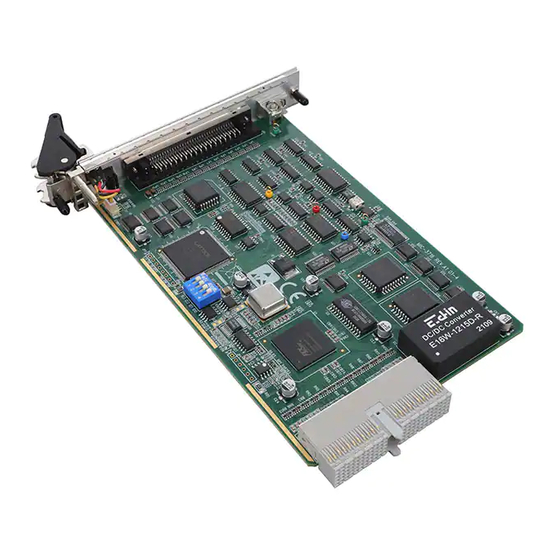
1. Introduction Thank you for buying the Advantech MIC-3716 CompactPCI (cPCI) card. The Advantech MIC-3716 is a powerful data acquisition (DAS) card which complies with PICMG 2.0 R2.1 CompactPCI specifications. It features a unique circuit design and complete functions for data acquisition and control, including A/D conversion, D/A conversion, digital input, digital output, and counter/timer. -
Page 13: Product Description
1.1 Product Description The Advantech MIC-3716 provides users with the most requested measurement and control functions as below: w CompactPCI bus specification 2.1 compliant w PCI-bus mastering for data transfer w 16-channel Single-Ended or 8 differential analog input w 16-bit A/D conversion with up to 250 KS/s sampling rate... - Page 14 On-board FIFO (First-In-First-Out) Memory The MIC-3716 provides an onboard FIFO memory buffer that can store 1K samples. Users can either enable or disable the interrupt request feature of the FIFO buffer. While the interrupt request for...
- Page 15 Board ID The MIC-3716 has a built-in DIP switch that helps define each card’ s ID when multiple cards have been installed on the same CompactPCI system. The board ID function is very useful when users build their system with multiple MIC-3716 cards.
-
Page 16: What You Need To Get Started
1.2 What You Need to Get Started Before you install your MIC-3716 card, please make sure you have the following necessary components: w MIC-3716 Multifunction card w MIC-3716 User’ s Manual w Driver software Advantech DLL drivers (included in the... -
Page 17: Fig. 1-1: Installation Flow Chart
Fig. 1-1: Installation Flow Chart... -
Page 18: Software Programming Choices
1.3 Software Programming Choices Advantech offers a rich set of DLL drivers, third-party driver support and application software to help fully exploit the functions of your MIC-3716 card: DLL driver (on the companion CD-ROM) LabVIEW driver Advantech ActiveDAQ Advantech GeniDAQ For more information on software, please refer to Chapter 4, Software Programming Overview. -
Page 19: Optional Accessories
1.4 Optional Accessories Advantech offers a complete set of accessory products to support the MIC-3716 cards. These accessories include: Wiring Cable n PCL-10168 The PCL-10168 shielded cable is specially designed for MIC-3716 cards to provide high resistance to noise. To achieve a better signal quality, the signal wires are twisted in such a way as to form a “twisted-pair cable”, reducing... - Page 20 connectors. The PCLD-8710 features the following functions: w Two additional 20-pin flat-cable connectors for digital input and output w Reserved space on the board to meet future needs for signal-conditioning circuits (e.g. low-pass filter, voltage attenuator and current shunt) w Industrial-grade screw-clamp terminal blocks for heavy-duty and reliable connections.
- Page 21 Installation and Configuration...
-
Page 22: Installation
This chapter gives users a package item checklist, proper instructions about unpacking and step-by-step procedures for both driver and card installation. 2.1 Unpacking After receiving your MIC-3716 package, please inspect its contents first. The package should contain the following items: þ MIC-3716 card þ Companion CD-ROM (DLL driver included) þ... - Page 23 After taking out the card, you should first: Inspect the card for any possible signs of external damage (loose or damaged components, etc.). If the card is visibly damaged, please notify our service department or our local sales representative immediately. Avoid installing a damaged card in your system.
-
Page 24: Software Installation
2.2 Software Installation We recommend you install the driver before you plug the MIC-3716 card into your system, since this will guarantee a smooth installation process. The 32-bit DLL driver Setup program for the MIC-3716 card is included on the companion CD-ROM that is shipped with your DAS card package. -
Page 25: Hardware Installation
Fig. 2-2: Different options for Driver Setup For further information on driver-related issues, an online version of the DLL Drivers Manual is available by accessing the following path: Start/ Programs/ Advantech Automation/ Device Manager/ Device Driver's Manual 2.3 Hardware Installation... - Page 26 Step 3: Holding the lower handle, pull the handle down to unlock it. Step 4: Insert the MIC-3716 card into the cPCI chassis carefully by sliding the lower edge of the card into the card guide.
- Page 27 Blue LED on the front panel will turn on. You can now slide the card out. Note : 1. Advantech MIC-3761’s “Hot-Swap” function complies with the cPCI Hot Swap Specification PICMG 2.1 R2.0. 2. Because of the “Hot-Swap”, the above steps detail the card removal process while the system is on.
- Page 28 2.2 Software Installation. After the MIC-3716 card is installed, you can verify whether it is properly installed on your system with the Device Manager: 1. Access the Device Manager through:...
-
Page 29: Fig. 2-3: The Device Name Listed On The Device Manager
Fig. 2-3: The device name listed on the Device Manager Note: If your card is properly installed, you should see the device name of your card listed on the Device Manager tab. If you do see your device name listed on it but marked with an exclamation sign “!”, it means your card has not been correctly installed. -
Page 30: Device Setup & Configuration
Step 1: To install the I/O device for your card, you must first run the Advantech Device Manager program by accessing: Start/ Programs/ Advantech Automation/ Device Manager/ Advantech Device Manager. Step 2: The Advantech Device Manager will search for the device(s) already installed on your system (if any) automatically. -
Page 31: Fig. 2-4: The Device Manager Dialog Box
Step 3: The Installed Devices box will list the device(s) found on your system, such as the one in Fig. 2-4. Fig. 2-4: The Device Manager dialog box... -
Page 32: Fig. 2-5: The Device Setting Dialog Box
Configuring the Device Step 4: In the Device Setting dialog box (Fig. 2-5), you can configure the voltage source either as External or Internal, and specify the voltage output range for the two D/A channels. Fig. 2-5: The Device Setting dialog box Note: w You can configure the source of D/A reference voltage either as Internal or External, and select the output voltage range. -
Page 33: Fig. 2-6: The Device Name Appearing On The List Of Devices Box
Note: As you can see from the above figure, the device name is: “000: <MIC-3716 BoardID=15 I/O=fd00H >”. Each device name begins with a device number (“000”), which is specifically assigned to each card. The device number is passed to the driver to specify which device you wish to... -
Page 34: Device Testing
An Advantech Device Test dialog box will appear accordingly (Fig. 2-7). Fig. 2-7: The Advantech Device Test dialog box In the Advantech Device Test dialog box, you can test various functions of MIC-3716 from the Analog input, Digital input, Digital output, Analog output or Counter tabs. -
Page 35: Fig. 2-8: Analog Input Tab On The Device Test Dialog Box
Note: n You can access the Advantech Device Test dialog box either by the previous procedure for the Advantech Device Manager or simply by accessing Start/Programs/ Advantech Automation/ Device Manager/ Advantech Device Manager. n All the functions are performed by the software polling method. For high speed data acquirement or output, they have to use corresponding VC examples like ADINT, ADDMA or ADBMDMA. -
Page 36: Fig. 2-9: Analog Output Tab On The Device Test Dialog Box
Testing the Analog Output Function Click the Analog Output tab to bring it up to the foreground. The Analog Output tab allows you to output quasi-sine, triangle, or square waveforms generated by the software automatically, or output single values manually. You can also configure the waveform frequency and output voltage range. -
Page 37: Fig. 2-10: Digital Input Tab On The Device Test Dialog Box
Testing the Digital Input Functions Click the Digital Input tab to show the Digital Input test panel as seen below in figure 2-10. Through the color of the lamps, you can discern whether the status of each digital input channel is either high or low. (Red = high, Green = low) Fig. -
Page 38: Fig. 2-11: Digital Output Tab On The Device Test Dialog Box
Testing the Digital Output Functions Click the Digital Output tab to bring up the Digital Output test panel such as the one seen on the next page. By pressing the buttons on each tab, you can set each digital output channel as high or low for the corresponding port. -
Page 39: Fig. 2-12: Counter Tab On The Device Test Dialog Box
Testing the Counter Function Click the Counter Tab to bring its test panel forth. The counter channel (Channel 0) offers two options: Event counting and Pulse out. If you select Event counting, you need to first connect your clock source to pin CNT0_CLK. The counter will start counting after the pin CNT0_GATE is triggered. - Page 40 (This page is left blank for hard printing.)
- Page 41 Signal Connections...
-
Page 42: Signal Connections
MIC-3716 via the I/O connector. 3.2 I/O Connector The I/O connector on the MIC-3716 is a 68-pin connector that enables you to connect to accessories with the PCL-10168 shielded cable. Note: The PCL-10168 shielded cable is especially designed for the MIC-3716 to reduce noise in the analog signal lines. - Page 43 The three ground references AIGND, AOGND, and DGND should each be used discreetly according to their designated purpose. An individual GND pin is available for AI, AO and DIO to provide optimum signal quality. Since all the signals on the DAS card need to refer to the same GND, the manufacturer has tested and chosen the best point to connect AIGND, AOGND and DGND together.
-
Page 44: Fig. 3-1: I/O Connector Pin Assignments For The Mic-3716
Fig. 3-1: I/O connector pin assignments for the MIC-3716... -
Page 45: Table 3-1: I/O Connector Signal Description
I/O Connector Signal Description Table 3-1: I/O Connector Signal Description Signal Name Reference Direction Description Analog Input Channels 0 through 15. Each channel pair, AI<0… 15> AIGND Input AI<i, i+1> (i = 0, 2, 4...14), can be configured as either two single-ended inputs or one differential input. -
Page 46: Analog Input Connections
A signal source without a local ground is also called a “floating source”. It is fairly simple to connect a single-ended channel to a floating signal source. In this mode, the MIC-3716 provides a reference ground for external floating signal sources. Fig. 3-2 shows a single-ended channel connection between a floating signal source and an input channel on the MIC-3716. -
Page 47: Fig. 3-2: Single-Ended Input Channel Connection
The differential input channels operate with two signal wires for each channel, and the voltage difference between both signal wires is measured. On the MIC-3716, when all channels are configured to differential input, up to 8 analog channels are available. -
Page 48: Fig. 3-3: Differential Input Channel Connection - Ground Reference Signal
Low input. Fig. 3-3 shows a differential channel connection between a ground-reference signal source and an input channel on the MIC-3716. With this connection, the PGIA rejects a common-mode voltage V... -
Page 49: Fig. 3-4: Differential Input Channel Connection - Floating Signal Source
MIC-3716. In this figure, each side of the floating signal source is connected through a resistor to the AIGND. This connection can reject the common-mode voltage between the signal source and the MIC-3716 ground. -
Page 51: Analog Output Connections
3.4 Analog Output Connections The MIC-3716 provides two D/A output channels, AO0_OUT and AO1_OUT. You may use the MIC-3716 internally-provided precision -5V (-10V) reference to generate a 0 to +5 V (+10 V) D/A output range. You may also create a D/A output range through external references, AO0_REF and AO1_REF. -
Page 52: Trigger Source Connections
32-bit timer for pacer triggering. A low-to-high edge from the Counter 2 output (PACER_OUT) will trigger an A/D conversion on the MIC-3716. At the same time, you can also use this signal as a synchronous signal for other applications. - Page 53 MIC-3716. The signal cables must be kept away from strong electromagnetic sources such as power lines, large electric motors, circuit breakers or welding machines, since they may cause strong electromagnetic interference. Keep the analog signal cables away from any video monitor, since it can significantly affect a data acquisition system.
- Page 54 (This page is left blank for hard printing.)
- Page 55 Software Programming Overview...
-
Page 56: Software Programming Overview
DLL Driver The Advantech DLL Drivers software is included on the companion CD-ROM. It also comes with all Advantech DAS cards. Advantech’ s DLL driver features a complete I/O function library to help boost your application performance. The Advantech DLL driver for Windows 95/98/NT/2000/XP works seamlessly with development tools such as Visual C++, Visual Basic, Borland C++ Builder and Borland Delphi. -
Page 57: Dll Driver Programming Roadmap
Since register-level programming requires much effort and time, we recommend that you use the Advantech DLL drivers instead. However, if register-level programming is indispensable, you should... - Page 58 2000/XP Application with DLL Driver chapter and the Function Overview chapter on the DLL Drivers Manual. Programming with the DLL Driver Function Library The Advantech DLL driver offers a rich function library to be utilized in various application programs. This function library consists of...
- Page 59 numerous APIs that support many development tools, such as Visual C++, Visual Basic, Delphi and C++ Builder. According to their specific functions or services, the APIs can be categorized into several function groups: w Analog Input Function Group w Analog Output Function Group w Digital Input/Output Function Group w Counter Function Group w Temperature Measurement Function Group...
- Page 60 (This page is left blank for hard printing.)
- Page 61 Calibration...
-
Page 62: Calibration
If you installed the program to another directory, you can find these programs in the corresponding subfolders in your destination directory. The MIC-3716 has been calibrated at the factory for initial use. However, a calibration of the analog input and the analog output functions every six months is recommended. -
Page 63: Vr Assignment
\Program Files\ADVANTECH\ADSAPI\Utilities\MIC3716 5.2 VR Assignment There is one variable resistor (VR1) on the MIC-3716 to adjust the accurate reference voltage on the MIC-3716. We have provided a test point (See TP4 in Fig. 5-1) for you to check the reference voltage on board. -
Page 64: Auto-Calibration
D/A calibration. The program helps the user to easily finish the calibration procedures automatically; however, the user can calibrate the MIC-3716 manually. Appendix E illustrates the standard calibration procedure for your reference. If you want to calibrate the hardware in your own way, these two sections will guide you. The following steps will guide you through the MIC-3716 software calibration. -
Page 65: Fig. 5-2: Selecting The Device You Want To Calibrate
Note: If you installed the program to another directory, you can find this program in the corresponding subfolders in your destination directory. Step 2: Select MIC-3716 in the ADSDAQ dialog box. Fig. 5-2: Selecting the device you want to calibrate... -
Page 66: Fig. 5-3: Warning Message Before Start Calibration
Step 3: After you start to calibrate the MIC-3716, please don’t forget to adjust VR1. Fig. 5-3: Warning message before start calibration... -
Page 67: Fig. 5-4: Auto A/D Calibration Dialog Box
A/D channel Auto-Calibration Step 4: Click the Auto A/D Calibration tab to show the A/D channel auto-calibration panel (Fig. 5-4). Press the start button to calibrate A/D channels automatically. Fig. 5-4: Auto A/D Calibration Dialog Box Step 5: The first A/D calibration procedure is enabled (Fig. 5-5). Fig. -
Page 68: Fig. 5-6: A/D Calibration Procedure 2
Step 6: The second A/D calibration procedure is enabled (Fig. 5-6) Fig. 5-6: A/D Calibration Procedure 2 Step 7: The third A/D calibration procedure is enabled (Fig. 5-7) Fig. 5-7: A/D Calibration Procedure 3... -
Page 69: Fig. 5-8: A/D Calibration Is Finished
Please finish the A/D calibration procedure first before you start the D/A calibration procedure. There are two D/A channels in MIC-3716; select the output range for each channel and then press the start button to calibrate the D/A channels (Fig. 5-9). -
Page 70: Fig. 5-9: Range Selection In D/A Calibration
Fig. 5-9: Range Selection in D/A Calibration Step 10: D/A channel 0 calibration is enabled (Fig. 5-10) Fig. 5-10: Calibrating D/A Channel 0... -
Page 71: Fig. 5-11: Calibrating D/A Channel 1
Step 11: D/A channel 1 calibration is enabled (Fig. 5-11) Fig. 5-11: Calibrating D/A Channel 1 Step 12: Auto-calibration is finished (Fig. 5-12) Fig. 5-12: D/A Calibration is finished... -
Page 72: Manual Calibration
MIC-3716 can read. For example, if the input range is 0 ~ 5V, the input voltage should be 2.9992V not 3V. -
Page 73: Fig. 5-13: Selecting Input Rage In Manual A/D Calibration Panel
Fig. 5-13: Selecting Input Rage in the Manual A/D Calibration panel Step 2: Depending on the difference between reference voltage and the received data in MIC-3716, adjust the gain, bipolar offset and unipolar offset registers (Fig. 5-14) Fig. 5-14: Adjusting registers... - Page 74 Step 3: Adjust the registers until they fall between the input voltage from the standard voltage reference and the receiving voltage reflected in the Manual A/D Calibration tab. D/A channel Manual-Calibration Step 1: Click the Manual D/A Calibration tab to show the D/A channel manual calibration panel.
- Page 75 Step 2: For example, choose channel 0; select the Range and select the wished output voltage code or value from the radio buttons (Fig. 5-15 and Fig. 5-16). Fig. 5-15 & Fig. 5-16: Selecting D/A Range and Choosing Output Voltage...
-
Page 76: Fig. 5-17: Adjusting Registers
Step 3: According to the difference between the output voltage from D/A channel and the value in the multi-meter, adjust the gain, bipolar offset and unipolar offset registers (Fig. 5-17) Fig. 5-17: Adjusting registers Step 4: Adjust registers until they fall between the output voltage from the D/A channel and the value in the multi-meter. - Page 77 Appendixes...
-
Page 78: Appendix A. Specifications
Appendix A. Specifications Analog Input Channels 16 Single-Ended or 8rdiggerential or combination Resolution 16-bit FIFO Size 1K samples Max. Sampling 250 KS/s max. Rate Conversion Time 2.5 µs Gain Input range and Unipolar 0~10 0~2.5 0~1.25 Gain List ±5V ±2.5V ±1.25V ±0.625V Bipolar... - Page 79 Analog Output Channels Resolution 16-bit Operation mode Single output Throughput 200 KS/s max. per channel ( FSR) Using Internal 0 ~ +5V, 0 ~ +10V, - 5V ~ + 5V, - 10V ~ Output Range Reference +10V ( Internal & External 0 ~ +x V @ + x V ( - 10 ≦...
- Page 80 General I/O Connector Type 68-pin SCSI-II female Dimensions 175 mm x 100 mm ( 6.9” x 3.9” ) + 5 V @ 850mA Typical Power + 12V @ 600mA Consumption + 5 V @ 1 A Max. + 12V @ 700mA 0 ~ +60°C ( 32~ 158 ℉...
-
Page 81: Appendix B. Block Diagrams
Appendix B. Block Diagrams... - Page 82 (This page is left blank for hard printing.)
-
Page 83: Appendix C. Register Structure And Format
For example, BASE+0 is the card's base address and BASE+7 is the base address plus seven bytes. Table C-1 shows the function of each register of the MIC-3716 or driver and its address relative to the card's base address. -
Page 84: Table C-1: Mic-3716 Register Format (Part 1)
Table C-1: MIC-3716 register format (Part 1) Base Read Address +decimal A/D Data AD15 AD14 AD13 AD12 AD11 AD10 A/D Status Register AD16/12 CNT0 ONE/FH IRQEN GATE PACER D/A channel 0 data D/A channel 1 data... -
Page 85: Table C-1: Mic-3716 Register Format (Part 2)
Table C-1: MIC-3716 register format (Part 2) Base Read Address +decimal Digital Input DI15 DI14 DI13 DI12 DI11 DI10 Board ID Counter 0 Counter 1 Counter 2... -
Page 86: Table C-1: Mic-3716 Register Format (Part 3)
Table C-1: MIC-3716 register format (Part 3) Base Write Address +decimal Software A/D Trigger A/D Channel Range Setting Multiplexer Control Stop channel Start channel A/D Control Register CNT0 ONE/FH IRQEN GATE EXT0 PACER AD16/12 Clear Interrupt and FIFO Clear FIFO... -
Page 87: Table C-1: Mic-3716 Register Format (Part 4)
Table C-1: MIC-3716 register format (Part 4) Base Write Address +decimal Digital Output DO15 DO14 DO13 DO12 DO11 DO10 DOI9 Calibration Command and Data Counter 0 Counter 1 Counter 2 Counter Control... -
Page 88: Channel Number And A/D Data - Base+0 And Base+1
BASE+0 and BASE+1 hold the result of A/D conversion data. The 16 bits of data from the A/D conversion are stored in BASE+1 bit 7 to bit 0 and BASE+0 bit 7 to bit 0. Table C-2: MIC-3716 Register for A/D data Read A/D Data... -
Page 89: Software A/D Trigger - Base+0
C.4 Software A/D Trigger — BASE+0 You can trigger an A/D conversion by software, the card's on-board pacer or an external pulse. BASE+6, Bit 2 to bit 0, select the trigger source. (see Section C.7, Control Register -- BASE+6 ) If you select software triggering, a write to the register BASE+0 with any value will trigger an A/D conversion. -
Page 90: A/D Channel Range Setting - Base+2
C.5 A/D Channel Range Setting — BASE+2 Each A/D channel has its own input range, controlled by a gain code stored in the on-board RAM. To change the range code for a channel: w Write the same channel in BASE+4 (the start channel) and BASE+5 (the stop channel) (refer to Section C.6). -
Page 91: Table C-4: Gain Codes For Mic-3716
Table C-4: Gain codes for MIC-3716 Gain Code Gain Input Range(V) -5 to +5 -2.5 to +2.5 -1.25 to +1.25 -0.625 to +0.625 -10 to +10 0 to 10 0 to 5 0 to 2.5 0 to 1.25 Example: To set channel 3 as gain=1 1. -
Page 92: Mux Control - Base+4 And Base+5
C.6 MUX Control — BASE+4 and BASE+5 Table C-5: Register for multiplexer control Write Multiplexer Control Bit # BASE + 5 STO3 STO2 STO1 STO0 BASE + 4 STA3 STA2 STA1 STA0 STA3 ~ STA0 Start Scan Channel Number STO3 ~ STO0 Stop Scan Channel Number When you set the gain code of analog input channel n, you should set the Multiplexer start &... - Page 93 AI13, AI14, AI15, AI0, AI1, AI2, AI13, AI14, AI15, AI0, AI1, AI2, AI13, AI14... The scan logic of the MIC-3716 card is powerful and easily understood. You can set the gain code, B/U and S/D, for each channel.
- Page 94 When in single-ended mode, we can get data from AI0 and AI1 separately. But if we set them as differential mode, the results polling AI0 and AI1 will be the same. That is if we set the AI0 and AI1 as a differential input channel, we can get the correct result no matter if we poll channel 0 or channel 1.
- Page 95 Warning! Only even channels can be set as differential. An odd channel will become unavailable if its preceding channel is set as differential.
-
Page 96: Control Register - Base+6 And Base+7
C.7 Control Register — BASE+6 and BASE+7 The write-only register BASE+6 and BASE+7 allows users to set an A/D trigger source and an interrupt source. Table C-6: Control Register Write A/D Status Register Bit # BASE + 7 BASE + 6 AD16/12 CNT0 ONE/FH... -
Page 97: Table C-7: Mic-3716 Register For Channel Number And A/D Data
10 MH AD16/12 Analog Input resolution. 16 bit 12 bit. And those two registers BASE+0 & BASE+1 (Table C-7) Table C-7: MIC-3716 Register for channel number and A/D data Read Channel Number and A/D Data Bit # BASE + 1... - Page 98 CH3 ~ CH0 A/D Channel Number CH3 ~ CH0 hold the number of the A/D channel from which the data is received Analog I/O calibration bit Normal mode All analog input and outputs channels are connected to the 68 pin SCSI-II connector respectively.
-
Page 99: Status Register - Base+6 And Base+7
C.8 Status Register — BASE+6 and BASE+7 The registers of BASE+6 and BASE+7 provide information for A/D configuration and operation. Table C-8: Status Register Write A/D Control Register Bit # BASE + 7 BASE + 6 AD16/12 CNT0 ONE/FH IRQEN GATE PACER The content of the status register of BASE+6 is the same as that of the... -
Page 100: Clear Interrupt And Fifo - Base+8 And Base+9
Clear Interrupt C.10 D/A Output Channel 0 — BASE+10 and BASE+11 The MIC-3716 provides an innovative design as gate control for the Analog Output function. It works as a general Analog Output function when you disable the flag (bit 3 (DA0_LDEN) of BASE+14). That means data will be output immediately. -
Page 101: D/A Output Channel 0 - Base+10 And Base+11
C.11 D/A Output Channel 0 — BASE+10 and BASE+11 The write-only registers of BASE+10 and BASE+11 accept data for the D/A Channel 0 output. Table C-11: Register for D/A channel 0 data Write D/A Output Channel 0 Bit # BASE + 11 DA15 DA14 DA13... -
Page 102: D/A Output Channel 1 - Base+12 And Base+13
C.12 D/A Output Channel 1 — BASE+12 and BASE+13 The MIC-3716 provides an innovative design as gate control for the Analog Output function. It works as a general Analog Output function when you disable the flag (bit 11 (DA1_LDEN) of BASE+14). That means the data will be output immediately. -
Page 103: D/A Output Channel 1 - Base+12 And Base+13
C.13 D/A Output Channel 1 — BASE+12 and BASE+13 The write-only registers of BASE+12 and BASE+13 accept data for the D/A channel 1 output. Table C-13: Register for D/A channel 1 data Write D/A Output Channel 1 Bit # BASE + 13 DA15 DA14 DA13... -
Page 104: D/A Reference Control - Base+14
C.14 D/A Reference Control — BASE+14 The write-only register of BASE+14 allows users to set the D/A reference source. Table C-14: Register for D/A reference control Write D/A Output Channel 1 Bit # BASE + 15 DA1_LDEN DA1_I/E DA0_B/U DA1_5/10 BASE + 14 DA0_LDEN DA0/I/E DA0_B/U DA0_5/10 DAn_5/10... -
Page 105: Digital I/O Registers - Base+16 And Base+17
C.15 Digital I/O Registers — BASE+16 and BASE+17 The MIC-3716 offers 16 digital input channels and 16 digital output channels. These I/O channels use the input and output ports at addresses BASE+16 and BASE+17. Table C-15: Register for digital input... -
Page 106: Calibration Registers - Base+18 And Base+19
C.16 Calibration Registers — BASE+18 and BASE+19 The MIC-3716 offers Calibration registers BASE+16 and BASE+17 for calibrating A/D and D/A. Table C-17: Calibration Command and Data Register Write Calibration Command and Data Bit # BASE + 19 BASE + 18... -
Page 107: Table C-18: Calibration Command And Data Register
Table C-18: Calibration Command and Data Register Command Code Meaning A/D bipolar offset adjust A/D unipolar offset adjust PGA offset adjust A/D gain adjust D/A 0 gain 1 adjust (10 V) D/A 0 gain 2 adjust (5 V) D/A 0 bipolar offset adjust D/A 0 unipolar offset adjust D/A 1 gain 1 adjust (10 V) D/A 1 gain 2 adjust (5 V) -
Page 108: Board Id Registers - Base+20
C.17 Board ID Registers — BASE+20 The MIC-3716 offers Board ID register BASE+20. With correct Board ID settings, you can easily identify and access each card during hardware configuration and software programming. Table C-19: Register for Board ID Read Board ID... -
Page 109: Appendix D. 82C54 Counter Chip Function
Counter 0 On the MIC-3716, counter 0 can be a 16-bit timer or an event counter, selectable by users. When the clock source is set as an internal source, counter 0 is a 16-bit timer; when set as an external source, then counter 0 is an event counter and the clock source comes from CNT0_CLK. - Page 110 32-bit timer for the pacer trigger. A low-to-high edge of counter 2 output (PACER_OUT) will trigger an A/D conversion. At the same time, you can use this signal as a synchronous signal for other applications.
-
Page 111: Counter Read/Write And Control Registers
D.2 Counter Read/Write and Control Registers The 82C54 programmable interval timer uses four registers at addresses BASE + 24(Dec), BASE + 26(Dec), BASE + 28(Dec) and BASE + 30(Dec) for read, write and control of counter functions. Register functions appear below: Register Function BASE + 24(Dec) - Page 112 Description SC1 & SC0 Select counter Counter Read-back command RW1 & RW0 Select read / write operation Operation Counter latch Read/write LSB Read/write MSB Read/write LSB first, then MSB M2, M1 & M0 Select operating mode M1 M0 Mode Description Stop on terminal count Programmable one shot Rate generator...
- Page 113 BCD Select binary or BCD counting Type Binary counting 16-bits Binary coded decimal (BCD) counting If you set the module for binary counting, the count can be any number from 0 up to 65535. If you set it for BCD (Binary Coded Decimal) counting, the count can be any number from 0 to 9999.
- Page 114 The data format of the counter read/write register then becomes: BASE+24/26/28(Dec) Status read-back mode D6 D5 D3 D2 D1 D0 Value NC RW1 M2 M1 M0 BCD Current state of counter output Null count is 1 when the last count written to the counter register has been loaded into the counting element...
-
Page 115: Counter Operating Modes
D.3 Counter Operating Modes MODE 0 – Stop on Terminal Count The output will initially be low after you set this mode of operation. After you load the count into the selected count register, the output will remain low and the counter will count. When the counter reaches the terminal count, its output will go high and remain high until you reload it with the mode or a new count value. - Page 116 pulses, the present period will not be affected, but the subsequent period will reflect the value. The gate input, when low, will force the output high. When the gate input goes high, the counter will start from the initial count. You can thus use the gate input to synchronize the counter.
- Page 117 (N+1)/2 counts and low for (N-1)/2 counts. MODE 4 –Software-Triggered Strobe After the mode is set, the output will be high. When the count is loaded, the counter will begin counting. On terminal count, the output will go low for one input clock period then go high again. If you reload the count register during counting, the new count will be loaded on the next CLK pulse.
-
Page 118: Counter Operations
D.4 Counter Operations Read/Write Operation Before you write the initial count to each counter, you must first specify the read/write operation type, operating mode and counter type in the control byte and write the control byte to the control register [BASE + 30(Dec)]. - Page 119 latch commands, one for each counter latched. The read-back command can also latch status information for selected counter(s) by setting STA bit = 0. The status must be latched to be read; the status of a counter is accessed by a read from that counter. The counter status format appears at the beginning of the chapter.
- Page 120 (This page is left blank for hard printing.)
-
Page 121: Appendix E. Manual Calibration
(i.e. through software calibration) by executing the A/D calibration program AutoCali.EXE. Therefore, it is not necessary to adjust the hardware settings of the MIC-3716. However, the following calibration steps are also provided for your reference in case manual calibration is needed: 1. - Page 122 discrepancy is less then 2 LSB. 4. Adjust the BIPOLAR offset voltage. First, write any value to BASE+9 to clear FIFO. Then set the A/D channel to channel 0, and to set the range as –5 V to +5 V. 5.
-
Page 123: Table E-1: A/D Binary Code Table
9. Write the value from 0x0300 to 0x03FF sequentially to the Calibration Command and Data register (BASE+18), and get each bipolar range’ s data by the software trigger A/D method. Repeat this procedure 1000 times then average those data for each value. -
Page 124: D/A Calibration
1. Write 0x0400, 0x0500, 0x0600, 0x0700, 0x0800, 0x0900, 0x0A00 and 0x0B00 sequentially to the Calibration Command and Data register (BASE+18). Next, set the MIC-3716 to AI software trigger and calibration mode. After that, set the A/D channel to the corresponding D/A channel. That means, connect A/D channel 4 to D/A channel 0, and connect A/D channel 6 to D/A channel 1. - Page 125 D/A range as 0 V to 10 V. Next, write 0xFFFF to the corresponding D/A registers (BASE+10 and BASE+12). 3. Write the value from 0x0400 to 0x04FF sequentially to the Calibration Command and Data register (BASE+18), and get each bipolar range’ s data by the software trigger A/D method. Repeat this procedure 1000 times to average those data for each value.
- Page 126 7. Writing the value from 0x0600 to 0x06FF sequentially to the Calibration Command and Data register (BASE+18), and get each bipolar range’ s data by the software trigger A/D method. Repeat this procedure 1000 times to average those data for each value.
- Page 127 Table E-2: D/A binary code table A/D code Mapping Voltage Hex. Dec. Bipolar Unipolar 0000h 7FFFh 32767 -1 LSB 0.5 FS – 1 LSB 8000h 32768 0.5 FS FFFFh 65535 +FS – 1 LSB FS – 1 LSB Note n 1 LSB = FS / 65535 for Unipolar (For example: 1LSB = 10 / 65535, while the range is 0 V to10 V) n 1 LSB = +FS / 32768 for Bipolar (For example: 1LSB = 5 / 32768, while the range is –5 V to +5 V)
Need help?
Do you have a question about the MIC-3716 and is the answer not in the manual?
Questions and answers