Table of Contents
Advertisement
Quick Links
Advertisement
Table of Contents

Related Manuals for Advantech PCI-1723


Summary of Contents for Advantech PCI-1723
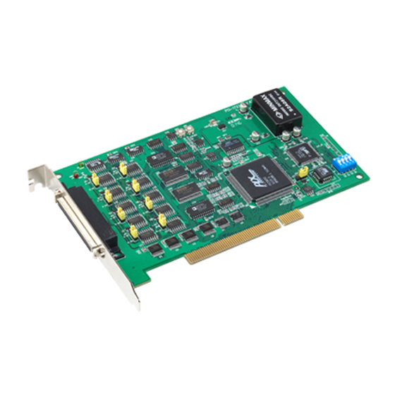
- Page 1 PCI-1723 16-bit, 8-ch., Non-Isolated Analog Output Card User Manual...
- Page 2 No part of this man- ual may be reproduced, copied, translated or transmitted in any form or by any means without the prior written permission of Advantech Co., Ltd. Information provided in this manual is intended to be accurate and reli- able.
- Page 3 Product Warranty (2 years) Advantech warrants to you, the original purchaser, that each of its prod- ucts will be free from defects in materials and workmanship for two years from the date of purchase. This warranty does not apply to any products which have been repaired or...
- Page 4 Before setting up the system, check that the items listed below are included and in good condition. If any item does not accord with the table, please contact your dealer immediately. Before you install your PCI-1723 card, please make sure you have the following necessary components: • PCI-1723 DA&C card •...
-
Page 5: Table Of Contents
Chapter 2 Installation ............. 12 Unpacking ..............12 Driver Installation ............13 Figure 2.1:Advantech Automation Software Setup ..13 Figure 2.2:Options for Driver Setup ......14 Hardware Installation ............. 15 Figure 2.3:Device Name on Device Manager ..... 16 Device Setup and Configuration ........17 2.4.1... - Page 6 Appendix C Register Structure & Format ....... 36 Overview ................ 36 I/O Port Address Map ........... 36 Table C.1:PCI-1723 Register Format ......37 D/A ch output data — BASE+00H~0EH ..... 41 D/A ch latch data — BASE+00H~0EH......42 Board ID — BASE+10H ..........43 All D/A Ch Synchronized Settings —...
- Page 7 Introduction This chapter gives background infor- mation on the PCI-1723. Sections include: • Features • Applications • Installation Guide • Software Overview • Device Driver Programming Road- • Accessories...
-
Page 8: Chapter 1 Introduction
Chapter 1 Introduction Thank you for buying the Advantech PCI-1723. The PCI-1723 is a non- isolated multiple channels analog output card for PCI bus, and each ana- log output channel is equipped with a 16-bit, double-buffered DAC. It features an auto-calibration function and Board ID. -
Page 9: Applications
Flexible Voltage Output Range The PCI-1723 provides a fixed voltage output range of °”10 V to fulfill your flexible range needed applications. Users can define the specific voltage output range and output data format via the enclosed software utility and driver. -
Page 10: Installation Guide
1.3 Installation Guide Before you install your PCI-1723 card, please make sure you have the following necessary components: • PCI-1723 DA&C card • PCI-1723 User’s Manual • Advantech DLL drivers (Included in the companion CD-ROM) • Wiring cable PCL-10168 (option) •... -
Page 11: Figure 1.1:Installation Flow Chart
Install Driver from CD -ROM, then power -off PC Install Hardware and power -on PC Use driver utility to configure hardware Use test utility to test hardware Read examples & driver manual Start to wri te your own application Figure 1.1: Installation Flow Chart Chapter 1... -
Page 12: Software Overview
Device Drivers The Advantech Device Drivers software is included on the companion CD-ROM at no extra charge. It also comes with all the Advantech DA&C cards. Advantech’s Device Drivers features a complete I/O function library to help boost your application performance. The Advantech... -
Page 13: Device Driver Programming Roadmap
• C++ Builder For instructions on how to begin programming works in each develop- ment tool, Advantech offers a Tutorial Chapter in the Device Drivers Manual for your reference. Please refer to the corresponding sections in this chapter on the Device Drivers Manual to begin your programming efforts. - Page 14 Drivers Manual. Programming with Device Drivers Function Library Advantech Device Drivers offer a rich function library that can be utilized in various application programs. This function library consists of numer- ous APIs that support many development tools, such as Visual C++, Visual Basic, Delphi and C++ Builder.
-
Page 15: Accessories
1.6 Accessories Advantech offers a complete set of accessory products to support the PCI- 1723 card. These accessories include: Wiring Cable PCL-10168 The PCL-10168 shielded cable is specially designed for PCI-1723 cards to provide high resistance to noise. To achieve a better signal quality, the signal wires are twisted in such a way as to form a “twisted-pair cable,”... - Page 16 PCI-1723 User Manual...
- Page 17 Installation This chapter gives users a package item checklist, proper instructions for unpacking and step-by-step procedures for both driver and card installation. Sections include: • Unpacking • Driver Installation • Hardware Installation • Device Setup and Configuration...
-
Page 18: Chapter 2 Installation
Chapter 2 Installation 2.1 Unpacking After receiving your PCI-1723 package, please inspect its contents first. The package should contain the following items: • PCI-1723 card • Companion CD-ROM (Device Drivers included) • User Manual The PCI-1723 card harbors certain electronic components vulnerable to electrostatic discharge (ESD). -
Page 19: Driver Installation
PC or transport it elsewhere. 2.2 Driver Installation We recommend you to install the driver before you install the PCI-1723 card into your system, since this will guarantee a smooth installation pro- cess. -
Page 20: Figure 2.2:Options For Driver Setup
Figure 2.2: Options for Driver Setup For further information on driver-related issues, an online version of the Device Drivers Manual is available by accessing the following path: Start/Programs/Advantech Device Drivers V2.0/Device Drivers Manual PCI-1723 User Manual... -
Page 21: Hardware Installation
Touch the metal part on the surface of your computer to neutralize the static electricity that might be on your body. Insert the PCI-1723 card into a PCI slot. Hold the card only by its edges and carefully align it with the slot. Insert the card firmly into place. -
Page 22: Figure 2.3:Device Name On Device Manager
After the PCI-1723 card is installed, you can verify whether it is properly installed on your system in the Device Manager: Access the Device Manager through Control Panel/System/Device Manager. The device name of the PCI-1723 should be listed on the Device Manager tab on the System Property Page. -
Page 23: Device Setup And Configuration
2.4 Device Setup and Configuration The Advantech Device Manager program is a utility that allows you to set up, configure and test your device, and later stores your settings on the system registry. These settings will be used when you call the APIs of Advantech Device Drivers. -
Page 24: Figure 2.5:"Device(S) Found" Dialog Box
Setting dialog box such as the one in Fig. 2-6. Figure 2.5: “Device(s) Found” Dialog Box 2.4.2 Configuring the Device On the Device Setting dialog box (Fig. 2-6), you can configure the voltage output range for the 8 D/A channels. Figure 2.6: Device Setting Dialog Box PCI-1723 User Manual... -
Page 25: Figure 2.7:Device Name On The List Of Devices Box
Figure 2.7: Device Name on the List of Devices Box Note: As we have noted, the device name “000:PCI-1723 BoardID=0 I/O=6500H” begins with a device number “000”, which is specifically assigned to each card. The device number is passed to the driver to specify which device you wish to control. - Page 26 Test… button to test your hardware by using the testing utility supplied. For more detailed information, please refer to Chapter 2 of the Device Drivers Manual. You can also find examples on the CD-ROM to speed up your program- ming. PCI-1723 User Manual...
- Page 27 Signal Connections This chapter gives an overview of the signal connections of PCI-1723. Sections include: • Overview • Switch and Jumper Settings • Signal Connections • Field Wiring Considerations...
-
Page 28: Chapter 3 Signal Connections
PCI- 1723 via the I/O connector. 3.2 Switch and Jumper Settings The PCI-1723 card has one function switch and five jumper settings. Figure 3.1: Card Connector, Jumper & Switches PCI-1723 User Manual... -
Page 29: Jp9
Complete loss of power to the chip clears the chip memory. Thus, no mat- ter how JP1 is set, if the power to the PCI-1723 is disconnected, the ana- log output initial power-on state will be "ZERO". -
Page 30: Board Id Setting
3.2.4 Board ID setting Board ID Note: On: 1, Off: 0 PCI-1723 User Manual... -
Page 31: Signal Connections
3.3 Signal Connections 3.3.1 Pin Assignment Figure 3-2 shows the pin assignments for the 68-pin I/O connector on the PCI-1723. Figure 3.2: I/O Connector Pin Assignments Chapter 3... -
Page 32: I/O Connector Signal Descriptions
Current Output, Channels 0 through 3. AGND Analog Ground. The two ground refer- ences (AGND and DGND) are con- nected together on the PCI-1723 card. DI0<0..15> DGND Digital Input / Output signals. These pins are digital input / Output channel 0 to 15. -
Page 33: Analog Output Connection
3.3.3 Analog Output Connection The PCI-1723 provides eight D/A output channels, Vout_0 ~ Vout_7 and Iout_0 ~ Iout_7. Users may use the PCI-1723 internally provided preci- sion -5V (-10 V) reference to generate 0 to +5 V (+10 V) D/A output range. -
Page 34: Field Wiring Considerations
3.4 Field Wiring Considerations When you use the PCI-1723 to acquire data from outside, noises in the environment might significantly affect the accuracy of your measure- ments if due cautions are not taken. The following measures will be help- ful to reduce possible interference running signal wires between signal sources and the PCI-1723. -
Page 35: Specifications
Specifications This appendix provides information on the specifications of PCI-1723. Sections include: • Analog Output • Digital Input/Output • General... -
Page 36: A.1 Analog Output
A.2 Digital Input /Output 16 (bi-directional) Input Channels Number of ports 0.8 V max. Input Voltage High 2.0 V min. 0.5 V max. @ +24 mA (sink) Output Voltage High 2.0 V min. @ -15 mA (source) PCI-1723 User Manual... -
Page 37: General
A.3 General I/O Connector Type 68-pin SCSI-II female 175 x 100 mm (6.9" x 3.9") Dimensions Typical +5 V @ 850 mA, +12 V @ 600 mA Power Consumption Max. +5 V @ 1 A, +12 V @ 700 mA Operation 0 ~ 60°... - Page 38 PCI-1723 User Manual...
-
Page 39: Block Diagram
Block Diagram This appendix shows the block diagram for PCI-1723. -
Page 40: Appendix B Block Diagram
Iout 3 16-Bit DAC 3 Vout 3 Iout 4 16-Bit DAC 4 Vout 4 Iout 5 16-Bit DAC 5 Vout 5 Iout 6 16-Bit DAC 6 Vout 6 Iout 7 16-Bit DAC 7 Vout 7 Auto Calibration Circuit PCI-1723 User Manual... - Page 41 Register Structure & Format This chapter provides information on the system settings of UNO-2052. Sections include: • Board Connectors and Jumpers • RS-232 Standard Serial Port • CAN Serial Port • Ethernet RJ-45 Connector • Phoenix Power Connector (PWR) • PS/2 Keyboard and Mouse Connector •...
-
Page 42: C.1 Overview
For example, BASE+0 is the card's base address and BASE+7 is the base address plus seven bytes. Table C-1 shows the function of each register of the PCI-1723 or driver and its address relative to the card's base address. -
Page 43: Table C.1:Pci-1723 Register Format
Table C.1: PCI-1723 Register Format Base PCI-1723 Register Format Adr. +HEX W D/A channel 0 output data R D/A channel 0 latch data W D/A channel 1 output data R D/A channel 1 latch data W D/A channel 2 output data... - Page 44 Table C.1: PCI-1723 Register Format W D/A channel 6 output data R D/A channel 6 latch data W D/A channel 7 output data R D/A channel 7 latch data W N/A R Board ID W All D/A channels synchronized setting...
- Page 45 R Digital I/O port mode W Write digital output command R Read digital input data W Write calibration command R Read calibration status Table C-1 PCI-1723 register format (Part 3) Base PCI-1723 Register Format Address 13 12 11 10 9 8 7...
- Page 46 Reset the calibration controller strobe X X X X X X X X Change D/A channels output type strobe X X X X X X X X Select the calibration Ref_V X X X X X X X X PCI-1723 User Manual...
-
Page 47: D/A Ch Output Data - Base+00H~0Eh
C.3 D/A ch output data — BASE+00H~0EH Table C-2 Register for D/A Channels Output Data Base 15 14 13 12 11 10 9 8 7 Addr. D/A channel 0 output data D/A channel 1 output data D/A channel 2 output data D/A channel 3 output data D/A channel 4 output data D/A Channel 5 output data... -
Page 48: D/A Ch Latch Data - Base+00H~0Eh
D/A channel 5 latch data D/A channel 6 latch data D/A channel 7 latch data DA15 ~ DA0 D/A channel latch data DA0 the least significant bit (LSB) of the D/A data DA15 the most significant bit (MSB) PCI-1723 User Manual... -
Page 49: Board Id - Base+10H
C.5 Board ID — BASE+10H The PCI-1723 offers Board ID register BASE+10H. With correct Board ID settings, users can easily identify and access each card during hard- ware configuration and software programming. Table C-4 Register for Board ID Base 15 14 13 12 11 10 9 Addr. -
Page 50: All D/A Ch Synchronized Settings - Base+12H
C.6 All D/A Ch Synchronized Settings — BASE+12H The PCI-1723 provides an innovate function in which all D/A channels can output their data in synchronization. Table C-5 Register for all D/A channels synchronized setting Base Addr. All D/A channels synchronized setting... -
Page 51: Dac Range & Calibration Mode - Base+14H
C.8 DAC Range & Calibration Mode — BASE+14H Table C-7 Register for DAC Range and Calibration Mode Base 15 14 13 12 11 10 9 Addr. DAC range and calibration mode R1 R0 O_ CH2 ~ CH0 Select D/A channel Channel 0 Channel 1 Channel 2... -
Page 52: Dac Range & Calibration Status - Base+14H
R1 R0 O_ CH2 ~ CH0 Select D/A channel Channel 0 Channel 1 Channel 2 Channel 3 Channel 4 Channel 5 Channel 6 Channel 7 Calibrate gain or offset Gain Offset R1 ~ R0 Select D/A range ± 10V PCI-1723 User Manual... -
Page 53: Sadc Control Command For Calibration Function-Base+16H
Change D/A channels output type and reload the parameters C.10 SADC Control Command for Calibration Func- tion— BASE+16H The PCI-1723 uses SADC (serial analog to digital converter) for the cali- bration function. Please refer to the Burr-Brown ADS7822 data sheet for the chipset detailed information (CD-ROM:\Documents\Component Specification\ ADS7822.PDF). -
Page 54: C.12 Calibration Parameter Strobe — Base+18H
Write any values to BASE+18H after finishing the calibration procedure to save all the D/A channels’ parameters into the EEPROM. Table C-11 Register for calibration parameter strobe Base 15 14 13 12 11 10 9 Addr. Calibration parameter strobe PCI-1723 User Manual... -
Page 55: Digital I/O Setting - Base+1Ah
Note: If you want to calibrate the range of the specific channel, be sure to write the value to BASE+14H first. Next, write the data to BASE+1EH for calibration purposes. Lastly, write the value to this register to strobe the parameters into EEPROM. -
Page 56: Digital I/O Port Mode - Base+1Ah
15 14 13 12 11 10 9 Addr. Write digital output command D9 D8 D7 D6 D5 D4 D3 D2 D1 D0 D15 ~ D0 Digital output data LSB of the output data MSB of the output data PCI-1723 User Manual... -
Page 57: Read Digital Input Data - Base+1Ch
C.16 Read Digital Input Data — BASE+1CH Table C-15 Register for Read Digital Input Data Base 15 14 13 12 11 10 9 Addr. Read digital input data D9 D8 D7 D6 D5 D4 D3 D2 D1 D0 D15 ~ D0 Digital input data LSB of the input data MSB of the input data C.17 Write Calibration Command —... -
Page 58: Read Calibration Status - Base+1Eh
15 14 13 12 11 10 9 Addr. Read calibration status D7 D6 D5 D4 D3 D2 D1 D0 D7 ~ D0 Calibration result data the least significant bit (LSB) of the data the most significant bit (MSB) PCI-1723 User Manual... -
Page 59: Synchronized Strobe - Base+20H
C.19 Synchronized Strobe — BASE+20H Write any values to BASE+20H to synchronize all D/A channels. Table C-18 Register for synchronized strobe Base 15 14 13 12 11 10 9 Addr. Synchronized strobe Note: Be sure to enable the synchronize function by writing the value to BASE+12H first. -
Page 60: Reset The Calibration Controller Strobe - Base+24H
Change D/A channels output type strobe Note: Once you want to change the range of the specific channel, be sure to write the value to BASE+14H first. After that, write any value to this register to strobe the change. PCI-1723 User Manual... -
Page 61: Select The Calibration Ref_V - Base+28H
C.23 Select the calibration Ref_V — BASE+28H Table C-22 Register for select the calibration Ref_V Base 15 14 13 12 11 10 9 Addr. Select the calibration Ref_V REF_A1 ~ REF_A0 Ref_V (reference voltage) index -10 V +10 V C.24 Summary Calibrate the range of the specific channel Step 1: BASE+14H Step 2: BASE+1EH... - Page 62 PCI-1723 User Manual...
Need help?
Do you have a question about the PCI-1723 and is the answer not in the manual?
Questions and answers