
Related Manuals for Advantech MIO-5393


Summary of Contents for Advantech MIO-5393
- Page 1 User Manual MIO-5393 ® ® 9th/8th Gen. Intel Xeon / Core™ H- series Processor, 3.5" MI/O- Compact SBC, DDR4, DP, HDMI, 48- bit LVDS, 2 GbE, M.2 E Key, M.2 B Key, MIOe...
- Page 2 No part of this manual may be reproduced, copied, translated or transmitted in any form or by any means without the prior written permission of Advantech Co., Ltd. Information provided in this manual is intended to be accurate and reliable. How- ever, Advantech Co., Ltd.
- Page 3 Because of Advantech’s high quality-control standards and rigorous testing, most of our customers never need to use our repair service. If an Advantech product is defec- tive, it will be repaired or replaced at no charge during the warranty period. For out- of-warranty repairs, you will be billed according to the cost of replacement materials, service time and freight.
- Page 4 Discard used batteries according to the manufacturer's instruc- tions. Technical Support and Assistance Visit the Advantech website at http://support.advantech.com where you can find the latest information about the product. Contact your distributor, sales representative, or Advantech's customer service center for technical support if you need additional assistance. Please have the following information ready before you call: –...
- Page 5 Packing List Before you begin installing your card, please make sure that the following materials have been shipped: 1 x MIO-5393 SBC 1 x SATA Cable 30cm (p/n: 1700006291) 1 x SATA Power Cable 35cm (p/n: 1700018785) ...
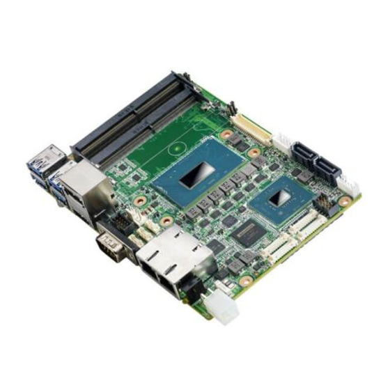
- Page 6 MIO-5393 User Manual...
-
Page 7: Table Of Contents
Environmental ................5 Block Diagram................... 5 Board Layout: Dimensions ................ 6 Figure 1.1 MIO-5393 Mechanical Drawing (Top Side) ....6 Figure 1.2 MIO-5393 Mechanical Drawing (Bottom Side) ... 6 Figure 1.3 MIO-5393 Mechanical Drawing (Coastline)....7 Figure 1.4 MIO-5393 Mechanical Drawing (with Cooler)..... 7 Figure 1.5 MIO-5393 Mechanical Drawing (with Heatsink) .. - Page 8 Table B.1: System I/O Ports ............86 DMA Channel Assignments ..............87 Table B.2: DMA Channel Assignments ........87 1st MB Memory Map................87 Table B.3: 1st MB Memory Map ..........87 Interrupt Assignments ................87 Table B.4: Interrupt Assignments ..........87 MIO-5393 User Manual viii...
-
Page 9: Chapter 1 General Information
Chapter General Information This chapter gives background information on the MIO-5393 Sections include: Introduction Specifications Block diagram Board layout and dimensions... -
Page 10: Introduction
Introduction MIO-5393 is designed using MI/O Extension form factor (compact series, 146 x 102 ® ® mm) and powered by 9th/8th generation of Intel Xeon /Core™ H series processors. MIO-5393 offers embedded iManager 3.0, SUSI 4.0 and WISE-PaaS/DeviceOn cre- ated by Advantech to monitor and control system operation effectively and remotely. - Page 11 Port2: i210 Gigabit Ethernet Controller Flow Control Support compliant with the 802.3X Specification Compliant with the 1 Gb/s IEEE 802.3 802.3u 802.3ab Specifications Magic Packet* wake-up enable with unique MAC address * Supports IEEE 1588 Peripheral Interface MIO-5393 User Manual...
-
Page 12: Os Support
– TPM2.0, only support under UEFI mode 1.2.2 OS Support MIO-5393 supports Win10 64 bit For further information about OS support of MIO-5393, please Advantech website: http://support.advantech.com.tw/ or contact the technical support center. 1.2.3 Mechanical Specifications Dimensions: 146 x 102 mm (5.7 x 4 inches) ... -
Page 13: Environmental
DDI x 1, PCIe x4, Audio Codec USB3.0/2.0 MIOe LPC, SMBUS, Rest, Line out, Power on Line-in/Out/MIC SMBus 256MB BIOS EIO-IS201 TPM 2.0 CAN Bus 2 x 8-bit GPIO COM1 RS-232/422/485 COM2 RS-232/422/485 *Function block with dotted line support by request MIO-5393 User Manual... -
Page 14: Board Layout: Dimensions
Board Layout: Dimensions Figure 1.1 MIO-5393 Mechanical Drawing (Top Side) Figure 1.2 MIO-5393 Mechanical Drawing (Bottom Side) MIO-5393 User Manual... - Page 15 Figure 1.3 MIO-5393 Mechanical Drawing (Coastline) Figure 1.4 MIO-5393 Mechanical Drawing (with Cooler) MIO-5393 User Manual...
- Page 16 Figure 1.5 MIO-5393 Mechanical Drawing (with Heatsink) Figure 1.6 MIO-5393 Mechanical Drawing (with Heat Spreader) MIO-5393 User Manual...
-
Page 17: Chapter 2 Installation
Chapter Installation This chapter explains the setup procedures of the MIO-5393 hard- ware, including instructions on setting jumpers and connecting peripherals, switches and indica- tors. Be sure to read all safety pre- cautions before you begin the installation procedure. -
Page 18: Jumpers & Switches
Jumpers & Switches The MIO-5393 has a number of jumpers that allow you to configure your system to suit your application. The table below lists the functions of the various jumpers. Table 2.1: Jumpers & Switches Clean CMOS Auto Power on Setting... -
Page 19: Locating Connectors & Block Diagram
Locating Connectors & Block Diagram CN18 CN28 CN29 CN30 CN17 CN15 CN14 CN13 CN10 CN7 CN31 CN27CN11 Figure 2.1 MIO-5393 Connector Locations (Top Side) CN19 CN21 CN22 CN33 CN24 Figure 2.2 MIO-5393 Connector Locations (Bottom Side) CN20 CN26 CN25 CN16 CN12 Figure 2.3 MIO-5393 Connector Locations (Coastline) -
Page 20: Setting Jumpers
Table 2.3: Clear CMOS (J1) Setting Function (1-2)* Normal (*Default) (2-3) Clear COMS 2.4.2 Auto Power On Setting (J2) Table 2.4: Auto Power On Setting (J2) Setting Function Power Button for Power On (1-2)* Auto Power On (*Default) MIO-5393 User Manual... -
Page 21: Com1 Power Setting (J3)
Table 2.6: LVDS VCON Setting (J4) Setting Function (1-3)* +3.3V (*Default) (3-5) (3-4) +12V 2.4.5 LVDS VCON Setting (J5) Table 2.7: LVDS VCON Setting (J5) Setting Function (1-2) 3.3V High for VCON on LVDS (2-3) * Low for VCON on LVDS (*Default) MIO-5393 User Manual... - Page 22 MIO-5393 User Manual...
-
Page 23: Chapter 3 Ami Bios Setup
Chapter AMI BIOS Setup... - Page 24 AMIBIOS has been integrated into many motherboards for over a decade. With the AMIBIOS Setup program, you can modify BIOS settings and control the various sys- tem features. This chapter describes the basic navigation of the MIO-5393 BIOS setup screens.
-
Page 25: Entering Setup
BIOS supports your CPU. If there is no number assigned to the patch code, please contact an Advantech application engineer to obtain an up-to-date patch code file. This will ensure that your CPU‘s system status is valid. -
Page 26: Advanced Bios Features Setup
3.1.2 Advanced BIOS Features Setup Select the Advanced tab from the MIO-5393 setup screen to enter the Advanced BIOS Setup screen. You can select any of the items in the left frame of the screen, such as CPU Configuration, to go to the sub menu for that item. You can display an Advanced BIOS Setup option by highlighting it using the <Arrow>... - Page 27 3.1.2.1 RC ACPI Settings Low Power S0 Idle Capability Determine if Enable ACPI Low Power S0 Idle Capability. MIO-5393 User Manual...
- Page 28 This item allows users to set how many processor cores should be active. Enable/Disable AES (Advanced Encryption Standard). MachineCheck Enable/Disable Machine Check. MonitorMWait Enable/Disable MonitorMWait. Intel Trusted Execution Technology ® Enables utilization of additional hardware capability provided by Intel Trusted Exe- cution Technology. MIO-5393 User Manual...
- Page 29 3.1.2.3 Power & Performance CPU – Power Management Control CPU – Power Management Control Options. GT – Power Management Control GT – Power Management Control Options. CPU - Power Management Control MIO-5393 User Manual...
- Page 30 Platform PL2 Enable Enable/Disable Platform Power Limit 1 programming. Power Limit 4 Override Enable/Disable Power Limit 4 override. C States Enable/Disable CPU Power Management. PowerLimit 3 Settings Power Limit 3 Settings. CPU Lock Configuration CPU Lock Configuration. MIO-5393 User Manual...
- Page 31 View/Configure Turbo Options Energy Efficient P-state Enable/Disable Energy Efficient P-state feature. Package Power Limit MSR Lock Enable/Disable locking of Package Power Limit settings. Energy Efficient Turbo Enable/Disable Energy Efficient Turbo feature. MIO-5393 User Manual...
- Page 32 Config TDP Configurations Configurable TDP Boot Mode Configurable TDP Mode as Nominal/Up/Down/Deactivate TDP selection. Configurable TDP Lock Configurable TDP Mode Lock sets the Lock bit. CTDP BIOS Control Enables CTDP control via runtime ACPI BIOS method. MIO-5393 User Manual...
- Page 33 Power Limit 3 Settings Power Limit 3 Override Enable/Disable Power Limit 3 override. MIO-5393 User Manual...
- Page 34 CPU Lock Configuration CFG Lock Configure MSR 0xE2[15], CFG Lock bit. Overclocking Lock Enable/Disable Overclocking Lock (BIT 20) in FLEX_RATIO(194) MSR. MIO-5393 User Manual...
- Page 35 GT - Power Management Control RC6(Render Standby) Check to enable render standby support. Maximum GT Frequency Maximum GT frequency limited by user. Disable Turbo GT Frequency Enabled/Disabled Turbo GT frequency. MIO-5393 User Manual...
- Page 36 MEBx setup. AMT Configuration ® Configure Intel Active Management Technology Parameters. ME Unconfig on RTC Clear When Disabled, ME will not be unconfigured on RTC Clear. Firmware Update Configuration Configure Management Engine Technology Parameters. MIO-5393 User Manual...
- Page 37 ACPI Sleep State Select the highest ACPI sleep state the system will enter when the SUSPEND button is pressed. Lock Legacy Resources Enables or Disables Lock of Legacy Resources. S3 Video Repost Enable or Disable S3 Video Repost. MIO-5393 User Manual...
- Page 38 Wake On Ring Control Enable/Disable Wake on Ring Function. Hardware Monitor Monitor hardware Status. Watch Dog Timer Configuration Watch Dog Timer Configuration Page. Case Open Detection Enable or Disable Case Open Detect Function. GPIO Configuration GPIO Configuration Settings. MIO-5393 User Manual...
- Page 39 Serial Port 1 Configuration Serial Port Enable or Disable Serial Port (COM). Change Settings Select an optimal settings for Super I/O device. COM Port Mode COM1 Port Mode Select. MIO-5393 User Manual...
- Page 40 Serial Port 2 Configuration Serial Port Enable or Disable Serial Port (COM). Change Settings Select an optimal settings for Super IO device. COM Port Mode COM2 Port Mode Select. MIO-5393 User Manual...
- Page 41 Hardware Monitor Watch Dog Timer Configuration Watch Dog Timer Enable or Disable Watch Dog Timer Function. MIO-5393 User Manual...
- Page 42 GPIO Configuration GPIO0/1/2/3/4/5/6/7/8/9/10/11/12/13/14/15 Configure GPIO0/1/2/3/4/5/6/7/8/9/10/11/12/13/14/15. MIO-5393 User Manual...
- Page 43 Select the TCG2 Spec Version Support. Physical Presence Spec Version Select to Tell O.S. to support PPI Spec Version 1.2 or 1.3. Device Select TPM 1.2 will restrict support to TPM 1.2 devices, TPM 2.0 will restrict support to TPM 2.0 devices. MIO-5393 User Manual...
- Page 44 3.1.2.8 S5 RTC Wake Settings Wake System from S5 Enable or disable System wake on alarm event. Select FixedTime, system will wake on the hr::min::sec specified. MIO-5393 User Manual...
- Page 45 3.1.2.9 Serial Port Console Redirection Console Redirection This item allows users to enable or disable console redirection for Microsoft Windows Emergency Management Services (EMS). Console Redirection This item allows users to configuration console redirection detail settings. MIO-5393 User Manual...
- Page 46 3.1.2.10 Intel TXT Information Intel TXT Information Display Intel TXT information. MIO-5393 User Manual...
- Page 47 Maximum time the device will take before it properly reports itself to the Host Control- ler. 'Auto' uses default value: for a Root port it is 100 ms, for a Hub port the delay is taken from Hub descriptor. MIO-5393 User Manual...
- Page 48 Controls the execution of UEFI and Legacy PXE OpROM. Storage Controls the execution of UEFI and Legacy Storage OpROM. Video Controls the execution of UEFI and Legacy Video OpROM. Other PCI Devices Determines OpROM execution policy for devices other than Network, Storage, or Video. MIO-5393 User Manual...
- Page 49 3.1.2.13 NVMe Configuration 3.1.2.14 Network Stack Configuration Network Stack Enable/Disable UEFI Network Stack. MIO-5393 User Manual...
-
Page 50: Chipset Configuration
3.1.3 Chipset Configuration Select the Chipset tab from the MIO-5393 setup screen to enter the Chipset BIOS Setup screen. You can display a Chipset BIOS Setup option by highlighting it using the <Arrow> keys. All Plug and Play BIOS Setup options are described in this sec- tion. - Page 51 X2APIC Opt Out Enable/Disable X2APIC Opt Out Bit. Memory Configuration Max TOLUD Maximum Value of TOLUD. Memory Scrambler Enable/Disable Memory Scrambler support. Force ColdReset Force ColdReset OR Choose MrcColdBoot mode. Memory Remap Enable/Disable Memory Remap above 4GB. MIO-5393 User Manual...
- Page 52 Select DVMT 5.0 Total Graphic Memory size used by the Internal Graphics Device. Gfx Low Power Mode This option is applicable for SFF only. PM Support Enable/Disable PM Spport. PAVP Enable Enable/Disable PAVP. CD Clock Frequency Select the highest Cd clock frequency supported by this platform. MIO-5393 User Manual...
- Page 53 Color Depth & Data Packing Color depth and data packing format for Non-EDID Support. Dual LVDS Mode Select LVDS bus to Single bus mode or Dual bus mode. LVDS Panel Type This item allow user to select LVDS panel type. MIO-5393 User Manual...
- Page 54 Enable or Disable onboard LAN's PXE option ROM. PCIE Wake Enable or Disable PCIE to wake the system from S5. State After S3 Specify what state to go to when power is re-applied after a power failure (G3 state). MIO-5393 User Manual...
- Page 55 PCI Express Configuration PCI Express Root Port 7/9/10/11/12/17 PCI Express Port 5/6/7/8/12/13 Settings. MIO-5393 User Manual...
- Page 56 Indicates the maximum speed the SATA controller can support. Software Feature Mask Configuration RST Legacy ROM/RST UEFI Driver will refer to the SWFM configuration to enable/ disable the storage feature. Aggressive LPM Support Enabled PCH to aggressively enter link power state. MIO-5393 User Manual...
- Page 57 USB Configuration XHCI Disable Compliance Mode Option to disable Compliance Mode. USB Port Disable Override Selectively Enable/Disable the corresponding USB Port from reporting a Device Con- nection to the Controller. MIO-5393 User Manual...
- Page 58 Security Configuration RTC Lock Enable will lock bytes 38h-3Fh in the lower/upper 128-byte bank of RTC RAM. BIOS Lock Enable or Disable the PCH BIOS Lock Enable feature. MIO-5393 User Manual...
- Page 59 HD Audio Configuration HD Audio Control Detection of the HD-Audio device. Disabled = HDA will be unconditionally disabled. Enabled = HDA will be unconditionally Enabled. MIO-5393 User Manual...
- Page 60 SerialIO Configuration I2C0 Controller Enable/Disables SerialIO Controller. MIO-5393 User Manual...
-
Page 61: Security
3.1.4 Security Select Security Setup from the MIO-5393 Setup main BIOS setup menu. All Security Setup options, such as password protection and virus protection are described in this section. To access the sub menu for the following items, select the item and press <Enter>:... -
Page 62: Boot
Enables or disables boot with initialization of a minimal set of devices required to launch active boot option. Has no effect for BBS boot options. New Boot Option Policy Controls the placement of newly detected UEFI boot options. MIO-5393 User Manual... -
Page 63: Save & Exit
This item allows you to save the changes done so far as user defaults. Restore User Defaults This item allows you to restore the user defaults to all the options. Boot Override Boot device select can override your boot priority. MIO-5393 User Manual... - Page 64 MIO-5393 User Manual...
-
Page 65: Chapter 4 Mioe Installation
Chapter MIOe Installation... -
Page 66: Quick Installation Guide
Here is the quick installation guide for our thermal design and MIOe module installation. Quick Installation Guide There is a Heatsink/Cooler (or optional heatspreader) in the white box inside the package, and please assembly it by following explosion drawing. 4.1.1 Cooler MIO-5393 User Manual... - Page 67 4.1.2 Heatsink 4.1.3 Heatspreader MIO-5393 User Manual...
- Page 68 MIO-5393 User Manual...
- Page 69 Appendix Pin Assignments This appendix contains informa- tion of a detailed or specialized nature Sections include: Jumper and Connector Tables...
- Page 70 Inverter Power output CN18 48 bit LVDS CN19 CN20 HDMI & DP++ CN21 M.2 E-key CN22 M.2 B/M-key CN24 NAMO SIM CN25 USB2.0+3.0_13H CN26 USB2.0+3.0_13H CN27 Internal USB CN28 SATA Power CN29 SATA_7V CN30 SATA_7V CN31 CN33 MIO-5393 User Manual...
- Page 71 Power Button for Power On (1-2)* Auto Power On Table A.5: J3 COM1 Power Settings Part Number 1653003201 Footprint HD_3x2P_79_D Description PIN HEADER 3x2P 2.0mm 180D(M) SMD 21N22050 Setting Function (1-2) (3-4) * Wake on Ring (5-6) +12V MIO-5393 User Manual...
- Page 72 Table A.8: CN1 12V Power Input Part Number 1655003865 Footprint WF_2x2P_165_BOX_RA_D_740SP Description ATX PWRCONN 2x2P 4.2mm 90D(M) DIP 740-77-04TS50 Pin Name +12V +12V Table A.9: CN3 SODIMMDDR4_260 9.2mm Part Number 1651002909-02 Footprint SODIMMDDR4_260P_AS0A826-HARB Description DDR4 SODIMM 260P/0.5mm/LCP/RA/G10u/S/BK/H9.2/RVS Pin Name MIO-5393 User Manual...
- Page 73 Table A.11: CN5 RTC Battery Part Number 1655005427-01 Footprint WF_2P_49_53398-0271 Description WAFER 2P 1.25mm 180D(M) SMD 53398-0271 Pin Name VBAT Table A.12: CN7 CAN BUS Part Number 1654903500 Footprint WHL3VS-125M Description WAFER 3P 1.25mm 90D(M) SMD 85205-03001 Pin Name CAN1_D+ CAN1_D- MIO-5393 User Manual...
- Page 74 Wafer 1x10P/1.25mm/PA/M/VA/WH/Sn/H4.7mm/WO Pin Name BUZZER- BUZZER+ RDC_CASEOPEN SATA_EXT_LED# PSIN# RST# HD LED +3.3V Power LED +5V Table A.14: CN9 Audio Part Number 1653007480-01 Footprint HD_5X2P_79_BOX_H245 Description BOXH 2x5P/2.0mm/LCP/M/VA/G10u/S/BK/H4.83/W CAP Pin Name LOUTR LINR LOUTL LINL MIC1R MIC1L MIO-5393 User Manual...
- Page 75 Part Number 1655904020 Footprint FPC4V-125M Description WAFER 4P 1.25mm 180D(M) SMD 85205-04001 Pin Name SMB0_DAT SMB0_CLK +V5_SMB Table A.16: CN11 I Part Number 1655904020 Footprint FPC4V-125M Description WAFER 4P 1.25mm 180D(M) SMD 85205-04001 Pin Name C_DAT C_CLK +V5_I MIO-5393 User Manual...
- Page 76 D-SUB 9P 2.77mm 90D(M) DIP G/F DSB5-09M1-KNR0-90 Pin Name COM_DCD# COM_RXD COM_TXD COM_DTR# COM_DSR# COM_RTS# COM_CTS# COM_RI# or 5/12V Table A.18: CN13 COM2 Part Number 1653007728-01 Footprint WF_10P_49_BOX_53398-1071 Description Wafer 1x10P/1.25mm/PA/M/VA/WH/Sn/H4.7mm/WO CAP Pin Name COM_RI# COM_DTR# COM_CTS# COM_TXD COM_RTS# COM_RXD COM_DSR# COM_DCD# MIO-5393 User Manual...
- Page 77 Table A.19: CN14 GPIO_P0 Part Number 1653007728-01 Footprint WF_10P_49_BOX_53398-1071 Description Wafer 1x10P/1.25mm/PA/M/VA/WH/Sn/H4.7mm/WO CAP Pin Name P0_GPIO7 P0_GPIO2 P0_GPIO6P P0_GPIO1 P0_GPIO5 P0_GPIO0 P0_GPIO4 P0_GPIO3 MIO-5393 User Manual...
- Page 78 Part Number 1653007728-01 Footprint WF_10P_49_BOX_53398-1071 Description Wafer 1x10P/1.25mm/PA/M/VA/WH/Sn/H4.7mm/WO CAP Pin Name P1_GPIO7 P1_GPIO2 P1_GPIO6 P1_GPIO1 P1_GPIO5 P1_GPIO0 P1_GPIO4 P1_GPIO3 Table A.21: CN16 RJ45_2x1_W/XFMR&LED Part Number 1652003274 Footprint RJ45_28P_RTB-19GB9J1A Description PHONE JACK RJ45 28P DIP RTB-19GB9J1A Pin Name MIO-5393 User Manual...
- Page 79 Wafer 2x20P/1.25mm/(M)/NY9T/VA/GFL/S/WH/W Post Pin Name +12V or +5V or +3.3V +12V or +5V or +3.3V +12V or +5V or +3.3V +12V or +5V or +3.3V LVDS0_D0- LVDS1_D0- LVDS0_D0+ LVDS1_D0+ LVDS0_D1- LVDS1_D1- LVDS0_D1+ LVDS1_D1+ LVDS0_D2- LVDS1_D2- LVDS0_D2+ LVDS1_D2+ LVDS0_CLK- MIO-5393 User Manual...
- Page 80 Table A.23: CN18 48-bit LVDS Panel LVDS1_CLK- LVDS0_CLK+ LVDS1_CLK+ LVDS1_CLK LVDS1_DAT LVDS0_D3- LVDS1_D3- LVDS0_D3+ LVDS1_D3+ VCON MIO-5393 User Manual...
- Page 81 +12V or +5V or +3.3V +12V or +5V or +3.3V +12V or +5V or +3.3V eDP_HDP ENABKL eDP Inverter 12V or 5V eDP Inverter 12V or 5V eDP Inverter 12V or 5V eDP Inverter 12V or 5V MIO-5393 User Manual...
- Page 82 MIO-5393 User Manual...
- Page 83 Part Number 1654012663-01 Footprint NGFF_75P_APCI0163-P001A Description NGFF 75P/0.5mm/(F)/LCP/RA/GFL/S/BK/H8.5mm/E-key Pin Name Pin Name +3.3VSB USB_D+ +3.3VSB USB_D- BT_PCMCLK BT_PCMSYNC BT_PCMIN BT_PCMOUT PETp0 PETn0 PERp0 PERn0 REFCLK+ REFCLK- SUSCLK PERESET# CLKREQ# BT_DISABLE# PCIE_WAKE# W_DISABLE# I2C DAT I2C_CLK +3.3VSB +3.3VSB MIO-5393 User Manual...
- Page 84 0.5mm 90D(F) H=8.5 SMD 2E0BC21-S85BM-7H) B key Pin Nam M key Pin Name +3.3VSB +3.3VSB +3.3VSB +3.3VSB PCIe_RX4- POWER_OFF# USB7_P+ PCIe_RX4+ WWAN_DISABLE# USB7_P- PCIe_TX4- +3.3VSB PCIe_TX4+ +3.3VSB +3.3VSB PCIe_RX3- +3.3VSB PCIe_RX3+ PCIe_TX3- GNSS_DISABLE# PCIe_TX3+ PCIe_RX1- PCIe_RX2- UIM_RESET PCIe_RX1+ PCIe_RX2+ UIM_CLK MIO-5393 User Manual...
- Page 85 PCIe_TX2+ SATA_RX+ PCIe_RX1+ SATA_RX- PCIe_RX1- SATA_TX- PCIe_TX1- SATA_TX+ PCIe_TX1+ PLTRST# CLK _REQ# CLK _REQ# CLK _PCIE- CLK _PCIE- PCIE_WAKE# PCIE_WAKE# CLK _PCIE+ CLK _PCIE+ SIM_KEYB_DET PLTRST_BKEY # SUSCLK SUSCLK M2_SSD_PEDET M2_SSD_PEDET +3.3VSB +3.3VSB +3.3VSB +3.3VSB +3.3VSB +3.3VSB MIO-5393 User Manual...
- Page 86 Table A.28: CN24 NANO SIM Part Number 1654013206-01 Footprint SIM_6P_N080613-SICR10 Description Nano SIM Card 6P/1.27/(F)/LCP/RA/GFL/S/BK/H1.37 Pin Name Table A.29: CN25 USB3.0_13H Part Number 1654013480-01 Footprint USB_9X2P_USB5-18F5-BNR0-10 Description USB 3.1 2x9P/2.0mm/PA66/(F)/RA/G30u/D/BU/H15.69 Pin Name MIO-5393 User Manual...
- Page 87 Table A.30: CN26 USB3.0_13H Part Number 1654013480-01 Footprint USB_9X2P_USB5-18F5-BNR0-10 Description USB 3.1 2x9P/2.0mm/PA66/(F)/RA/G30u/D/BU/H15.69 Pin Name Table A.31: CN27 Internal USB Part Number 1653007480-01 Footprint HD_5X2P_79_BOX_H245 Description BOXH 2x5P/2.0mm/LCP/M/VA/G10u/S/BK/H4.83/W CAP Pin Name A_D- B_D- A_D+ B_D+ MIO-5393 User Manual...
- Page 88 WAFER BOX 4P 2.50mm 180D(M) DIP 24W1170-04S10-01 Pin Name +12V Table A.33: CN29 SATA_7V Part Number 1654013615-01 Footprint SATA_7P_WATF-07DBN6SB1U Description SATA 7P/1.27mm/LCP/F/VA/G15u/S/BK/H8.41/W Post Pin Name Table A.34: CN30 SATA_7V Part Number 1654013615-01 Footprint SATA_7P_WATF-07DBN6SB1U Description SATA 7P/1.27mm/LCP/F/VA/G15u/S/BK/H8.41/W Post Pin Name MIO-5393 User Manual...
- Page 89 FAN_SPEED FAN_PWM Table A.36: CN33 MIOe Part Number 1654006235 Footprint BB_40x2P_32_1625x285_2HOLD Description B/B Conn. 40x2P 0.8mm 180D(F) SMD QSE-040-01-L-D Pin Name PCIE_RX0+ PCIE_TX0+ PCIE_RX0- PCIE_TX0- PCIE_RX1+ PCIE_TX1+ PCIE_RX1- PCIE_TX1- PCIE_RX2+ PCIE_TX2+ PCIE_RX2- PCIE_TX2- PCIE_RX3+ PCIE_TX3+ PCIE_RX3- PCIE_TX3- MIO-5393 User Manual...
- Page 90 Table A.36: CN33 MIOe PCIE_CLK+ LOUTL PCIE_CLK- LOUTR AGND SMB_CLK SMB_DAT PCIE_WAKE# RESET# SLP_S3# CLK24M LPC_AD0 DDP_HPD LPC_AD1 LPC_AD2 DDP_AUX+ LPC_AD3 DDP_AUX- LPC_SERIRQ DDP_D0+ LPC_FRAME# DDP_D0- USB0_D+ DDP_D1+ USB0_D- DDP_D1- USB1_D+ DDP_D2+ USB1_D- DDP_D2- USB2_D+ DDP_D3+ MIO-5393 User Manual...
- Page 91 Table A.36: CN33 MIOe USB2_D-- DDP_D3- USB_OC# +12VSB +12VSB +5VSB +5VSB +5VSB +5VSB MIO-5393 User Manual...
- Page 92 MIO-5393 User Manual...
- Page 93 Appendix System Assignments This appendix contains informa- tion of a detailed nature. Sections include: System I/O Ports DMA Channel Assignments 1st MB Memory Map Interrupt Assignments...
- Page 94 EC/PMC Controller 2F8h-2FFh Communications Port (COM2) 380h-3AFh Motherboard Resources 3C0h-3DFh Motherboard Resources 3F8h-3FFh Communications Port (COM1) 490h-4C7h Motherboard Resources 4D0h-4D1h Interrupt Controller 680h-69Fh Motherboard Resources A00h-AFFh Motherboard Resources 164Eh-164Fh Motherboard Resources 1800h-18FFh Motherboard Resources CF9h-CF9h Reset Generator MIO-5393 User Manual...
- Page 95 Communications Port (COM1) IRQ5 EC Watch DOG IRQ6 CANBus Controller IRQ7 Available IRQ8 System CMOS/real time clock IRQ9 Microsoft ACPI-Compliant System IRQ10 Available IRQ11 Display Controller IRQ12 Available IRQ13 Numeric data processor IRQ14 GPIO Controller IRQ15 Reserved MIO-5393 User Manual...
- Page 96 No part of this publication may be reproduced in any form or by any means, electronic, photocopying, recording or otherwise, without prior written permis- sion of the publisher. All brand and product names are trademarks or registered trademarks of their respective companies. © Advantech Co., Ltd. 2020...
Need help?
Do you have a question about the MIO-5393 and is the answer not in the manual?
Questions and answers