
Related Manuals for Altera Agilex 5 FPGA E Series


Summary of Contents for Altera Agilex 5 FPGA E Series
- Page 1 ™ Agilex 5 FPGA E-Series 065B Modular Development Kit User Guide 820977 Online Version Send Feedback 2024.07.12...
-
Page 2: Table Of Contents
Contents Contents 1. Overview........................4 1.1. Block Diagram.......................5 1.2. Feature Summary....................6 1.3. Box Contents......................7 1.4. Recommended Operating Conditions................ 7 2. Getting Started....................... 8 ® 2.1. Quartus Prime Software and Driver Installation............8 2.2. Quick Start Guide....................8 2.3. Design Examples....................9 3. - Page 3 Contents A.6. Memory Interfaces....................68 A.7. Board to Board Connector..................69 A.7.1. Modular Board Primary Connector.............. 69 A.7.2. Modular Board Secondary Connector............72 A.7.3. Carrier Board Primary Connector..............75 A.7.4. Carrier Board Secondary Connector............78 A.8. Communication Interfaces..................81 B. Additional Information....................83 B.1.
-
Page 4: Overview
Altera or Intel. Altera and Intel customers are advised to obtain the latest version of device specifications before relying on any published information and before placing orders for products or services. -
Page 5: Block Diagram
1. Overview 820977 | 2024.07.12 1.1. Block Diagram Figure 2. Agilex 5 FPGA E-Series 065B Modular Development Kit Block Diagram Modular Board HPS IO48 DDR4 x32 DDR4 x32 DDR4 x32 1GbE (HPS) Module GPIO COMP COMP COMP 2 Gb CFG Flash QSPI Uart (FPGA) JTAG... -
Page 6: Feature Summary
1. Overview 820977 | 2024.07.12 1.2. Feature Summary • Agilex 5 E-Series A5E065X device in 32 mm x 32 mm, 1591B Package — Dual core Arm* Cortex*-A76, Dual core Arm Cortex-A55 — 65K logic elements — High-voltage I/O (HVIO)-120 (6 banks) —... -
Page 7: Box Contents
1. Overview 820977 | 2024.07.12 1.3. Box Contents • Agilex 5 E-Series 065B Modular board (with heatsink) • Carrier board • 12V DC power adapter • RJ45 cable • Micro USB cable • Micro SD card Related Information Agilex 5 FPGA E-Series 065B Modular Development Kit Website More information about the Agilex 5 FPGA E-Series 065B Modular Development Kit documentation, including the Quick Start Guide and development kit unboxing video. -
Page 8: Getting Started
Altera or Intel. Altera and Intel customers are advised to obtain the latest version of device specifications before relying on any published information and before placing orders for products or services. -
Page 9: Design Examples
2. Getting Started 820977 | 2024.07.12 Related Information Agilex 5 FPGA E-Series 065B Modular Development Kit Website More information about the Agilex 5 FPGA E-Series 065B Modular Development Kit documentation, including the Quick Start Guide and development kit unboxing video. 2.3. -
Page 10: Development Kit Setup
Altera or Intel. Altera and Intel customers are advised to obtain the latest version of device specifications before relying on any published information and before placing orders for products or services. - Page 11 3. Development Kit Setup 820977 | 2024.07.12 Switch Default Position Function • ON—USER_DIPSW0 Low S7.1 • OFF—USER_DIPSW0 High • ON—USER_DIPSW1 Low S7.2 • OFF—USER_DIPSW1 High • ON—USER_DIPSW2 Low S7.3 • OFF—USER_DIPSW2 High • ON—Disable FMC JTAG mode S7.4 • OFF—Enable FMC JTAG mode 1PPS_MUX_SEL[1:0] •...
-
Page 12: Powering Up The Development Kit
3. Development Kit Setup 820977 | 2024.07.12 Switch Default Position Function MIPI 1 Vertical Sync (XVS) • ON—Enables Signal connection from Agilex 5 FPGA S11.1 device to MIPI1 Module • OFF—Disable Signal connection from Agilex 5 FPGA device to MIPI1 Module MIPI 1 Horizontal Sync (XHS) •... -
Page 13: Restoring Sd Card With The Default Factory Image
3. Development Kit Setup 820977 | 2024.07.12 3.3.2. Restoring SD Card with the Default Factory Image Note: The SD card is pre-programmed with sdimage. Completing the steps overwrites this image. Refer to RocketBoards.org to recover and update sdimage on SD card. 1. -
Page 14: Board Test System
Altera or Intel. Altera and Intel customers are advised to obtain the latest version of device specifications before relying on any published information and before placing orders for products or services. -
Page 15: Setting Up Bts Gui Running Environment
JTAG with other applications such as the Nios II JTAG Debug Module and the Signal Tap logic analyzer. Altera recommends closing other applications before using BTS, as the GUI is designed based on the Quartus Prime software. The BTS relies on the Quartus Prime software's specific library. Before running the BTS, open the Quartus Prime software to automatically set the environment variable QUARTUS_ROOTDIR. - Page 16 4. Board Test System 820977 | 2024.07.12 Figure 4. BTS Package Folder You can run BTS GUI with the following scripts. 1. On Windows system, double click the files to run BTS GUI. .bat 2. On Linux system, add current user to the group "dialout" to ensure the access to UART, using the following commands: # ls -l /dev/ttyUSB* # sudo usermod -a -G dialout $USER...
-
Page 17: Troubleshooting For Launching Bts
4. Board Test System 820977 | 2024.07.12 4.2. Troubleshooting for Launching BTS No Available Serial Ports Figure 6. Failure of "Could not find any available serial ports" 1. Check if the micro-USB is connected physically. 2. Check if the USB Serial Port driver is installed successfully. a. - Page 18 4. Board Test System 820977 | 2024.07.12 Figure 7. UART Port List No Response after Message Sent Figure 8. Failure of "sending msg is successful, but no response received" The issue roots that the UART does not work correctly or the Nios software in the System MAX 10 does not work well, follow the check list below: ™...
-
Page 19: Bts Functionalities
4. Board Test System 820977 | 2024.07.12 1. Check if the BTS is launched before the board is ready. 2. Check if there are some third-party UART tools that have occupied the port. 3. Check if there are other BTS instances and close them. 4. - Page 20 • Set: Sets the programmable oscillator frequency for the selected clock to the value in the OUTx output controls. Frequency changes might take several milliseconds to take effect. Altera recommends resetting the FPGA logic after changing frequencies. • Import: Imports the register list generated from the tool of the Skyworks* Clockbuilder Pro software.
- Page 21 4. Board Test System 820977 | 2024.07.12 • Status: Displays more detail status. • Default: Sets the frequency for the oscillator associated with the active tab back to its default value. This can also be accomplished by power cycling the board. •...
- Page 22 4. Board Test System 820977 | 2024.07.12 4.3.1.3. Si549 Figure 12. The Si549 Setting Page • Read: Reads the current frequency setting for the oscillator associated with the active tab. • Set: Sets the programmable oscillator frequency for the selected clock to the value in the output controls.
- Page 23 4. Board Test System 820977 | 2024.07.12 4.3.1.4. Si569 Figure 13. The Si569 Setting Page Note: This tab has similar control functions as the Si549 tab. 4.3.1.5. Si52202 Figure 14. The Si52202 Setting Page ™ Agilex 5 FPGA E-Series 065B Modular Development Kit User Guide Send Feedback...
-
Page 24: The Power Functionality
4. Board Test System 820977 | 2024.07.12 Note: The output frequency of Si52202 is fixed to 100 MHz. The GUI supports for enabling or disabling the output, and changing the output amplitude and spread enable. 4.3.2. The Power Functionality The Power Monitor tool reports most power rails’ voltage, current, and power information on the board. - Page 25 4. Board Test System 820977 | 2024.07.12 Figure 16. Power Tab—Modular Board Display Configure • Speed Adjustment: Adjusts the update rate of the current curve. • Select Board Type: Select to show the rails of the Carrier or Modular board. •...
- Page 26 4. Board Test System 820977 | 2024.07.12 4.3.2.2. Temperature Monitor Figure 17. Temperature Tab The BTS can monitor the temperature and presents the data visually. The BTS can also show the locations of the temperature sensors in main interface. ™ Agilex 5 FPGA E-Series 065B Modular Development Kit User Guide Send Feedback...
-
Page 27: The Max 10 Functionality
4. Board Test System 820977 | 2024.07.12 4.3.3. The MAX 10 Functionality The Agilex 5 FPGA E-Series 065B Modular Development Kit uses a MAX 10 as Board Management Control (BMC) master. It provides you with a UART based controller to power cycle the Modular board and set the MSEL. - Page 28 4. Board Test System 820977 | 2024.07.12 4.3.3.2. The IO Control Tab Figure 19. IO Control Tab You can use MSEL to set the configuration mode of the Agilex 5 FPGA device. The MSEL functions like a real DIP switch S4 on the board. The virtual switches only take effect when the physical switches are turned off.
-
Page 29: Agilex 5 Fpga Functionality
4. Board Test System 820977 | 2024.07.12 4.3.4. Agilex 5 FPGA Functionality While using the BTS, you reconfigure the FPGA several times with test designs specific to the functionality that you are testing. The BTS is also useful as a reference for designing systems. - Page 30 4. Board Test System 820977 | 2024.07.12 1. On the Configure menu, click the Configure command that corresponds to the functionality you want to test. 2. In the dialog box that appears, click Configure to download the corresponding design's SRAM Object File ( ) to the FPGA.
- Page 31 4. Board Test System 820977 | 2024.07.12 • Jtag Cable: Displays the cable name of the board. • Downloaded SOF: Indicates the design name which have been downloaded to the FPGA device. • Loaded design: Indicates the design name which have been loaded to System Console.
- Page 32 4. Board Test System 820977 | 2024.07.12 4.3.4.3.1. The FMC+ Tab The FMC+ Test Tab Figure 22. The FMC+ Test Tab Use the following controls to select an interface to apply PMA settings, data type and error control. Port Allows you to specify which interface to test. The following port test is available: •...
- Page 33 4. Board Test System 820977 | 2024.07.12 • Serial Loopback: Displays the signal status between the transmitter and the receiver. • VOD: Specifies the voltage output differential of the transmitter buffer. • Pre-emphasis tap: — Pre-tap 1: Specifies the amount of pre-emphasis on the first pre-tap of the transmitter buffer.
- Page 34 4. Board Test System 820977 | 2024.07.12 • Detected Errors: Displays the number of data errors detected in the received bit stream. • Inserted Errors: Displays the number of errors inserted into the transmit data stream. • Bit Error Rate: Calculates the bit error rate of the transmit data stream. •...
- Page 35 4. Board Test System 820977 | 2024.07.12 The FMC+ Status Tab Figure 25. The FMC+ Status Tab The Status Tab displays the following status information during the loopback test: • PLL Lock: Shows the PLL locked or unlocked state. • Pattern Sync: Shows the pattern synced or not state.
- Page 36 4. Board Test System 820977 | 2024.07.12 Figure 26. FMC+ Status—PLL and Pattern Status 4.3.4.3.2. The SFP+ Tab This tab has similar control functions as the FMC+ tab. ™ Agilex 5 FPGA E-Series 065B Modular Development Kit User Guide Send Feedback...
- Page 37 4. Board Test System 820977 | 2024.07.12 Figure 27. The SFP+ Test Tab ™ Agilex 5 FPGA E-Series 065B Modular Development Kit User Guide Send Feedback...
- Page 38 4. Board Test System 820977 | 2024.07.12 Figure 28. The SFP+ Status Tab ™ Agilex 5 FPGA E-Series 065B Modular Development Kit User Guide Send Feedback...
- Page 39 4. Board Test System 820977 | 2024.07.12 4.3.4.4. The Memory Tab This tab allows you to read and write DDR4-COMP memory on your board. Download the design through BTS Configure. 4.3.4.4.1. The COMP0 Tab The COMP0 Test Tab Figure 29. The COMP0 Test Tab The following sections describe controls on this tab.
- Page 40 4. Board Test System 820977 | 2024.07.12 The COMP0 Control Tab Figure 30. The COMP0 Control Tab—Traffic Generator • Test Size: You can choose the size of the memory to test. The available options are 64 KB, 256 KB, 1 MB, 4 MB, 16 MB, 64 MB, 256 MB, 1 GB, 4 GB, and 8 GB (default).
- Page 41 4. Board Test System 820977 | 2024.07.12 4.3.4.4.2. The COMP1 Tab The COMP1 tab shares the same settings with the DDR4 COMP0 tab. Figure 31. The COMP1 Test Tab ™ Agilex 5 FPGA E-Series 065B Modular Development Kit User Guide Send Feedback...
- Page 42 4. Board Test System 820977 | 2024.07.12 Figure 32. The COMP1 Control Tab—Traffic Generator ™ Agilex 5 FPGA E-Series 065B Modular Development Kit User Guide Send Feedback...
- Page 43 4. Board Test System 820977 | 2024.07.12 4.3.4.4.3. The HPS COMP Tab The HPS COMP tab shares the same settings with the DDR4 COMP0 tab. Figure 33. The HPS COMP Test Tab ™ Agilex 5 FPGA E-Series 065B Modular Development Kit User Guide Send Feedback...
- Page 44 4. Board Test System 820977 | 2024.07.12 Figure 34. The HPS COMP Control Tab—Traffic Generator ™ Agilex 5 FPGA E-Series 065B Modular Development Kit User Guide Send Feedback...
-
Page 45: Other Functionalities
4. Board Test System 820977 | 2024.07.12 4.3.5. Other Functionalities 4.3.5.1. The Diagnostic Functionality The Diagnostic menu provides the functionality of checking the status of the main devices on the Carrier and Modular boards. To trigger a basic board diagnostic, click the start button. - Page 46 4. Board Test System 820977 | 2024.07.12 4.3.5.2. The Sys Info The Sys Info menu presents the basic system information of the development kit. • Board Name: The official development kit board name. • Board Revision: The board hardware version. •...
- Page 47 4. Board Test System 820977 | 2024.07.12 4.3.5.3. The Connection Information The Connection menu presents the current connection information. • UART Port: The current recognized and activated UART port. • UART Baud Rate: The baud rate of the UART, with a fixed value of 115200, could not be configured.
- Page 48 4. Board Test System 820977 | 2024.07.12 4.3.5.4. The Bottom Info Bar The bottom information bar shows the status of the UART connection, the recognized Quartus Prime software version. • UART: Shows if the board is connected to BTS successfully. •...
-
Page 49: Development Kit Hardware And Configuration
Altera or Intel. Altera and Intel customers are advised to obtain the latest version of device specifications before relying on any published information and before placing orders for products or services. -
Page 50: Custom Projects For The Development Kit
Altera or Intel. Altera and Intel customers are advised to obtain the latest version of device specifications before relying on any published information and before placing orders for products or services. - Page 51 6. Custom Projects for the Development Kit 820977 | 2024.07.12 PIN_SWIZZLE_CH0_DQS2=16,17,18,19,20,21,22,23; PIN_SWIZZLE_CH0_DQS3=24,25,26,27,28,29,30,31; PIN_SWIZZLE_CH0_ECC=0,2,6,4,1,3,7,5; ™ Agilex 5 FPGA E-Series 065B Modular Development Kit User Guide Send Feedback...
-
Page 52: Hps Boot
Altera or Intel. Altera and Intel customers are advised to obtain the latest version of device specifications before relying on any published information and before placing orders for products or services. -
Page 53: Document Revision History For The Agilex 5 Fpga E-Series 065B Modular Development Kit User Guide
Altera or Intel. Altera and Intel customers are advised to obtain the latest version of device specifications before relying on any published information and before placing orders for products or services. -
Page 54: Development Kit Components
Altera or Intel. Altera and Intel customers are advised to obtain the latest version of device specifications before relying on any published information and before placing orders for products or services. -
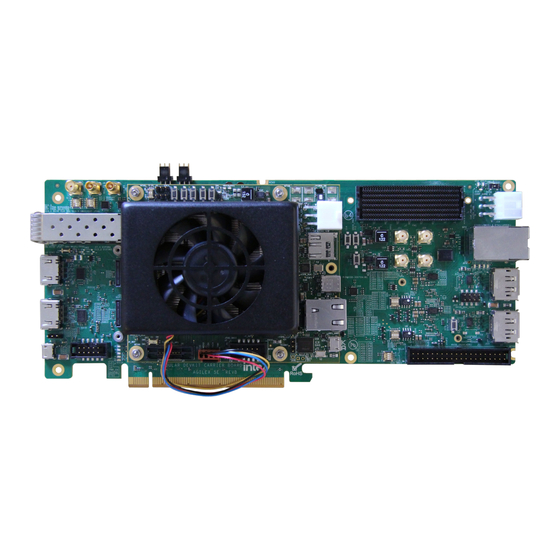
Page 55: Board Components
A. Development Kit Components 820977 | 2024.07.12 Figure 41. Modular Board (Top View) I2C Header-2 (J1) Standalone Power Input (J3) I2C Header-3 (J8) Micro SD Card Connector (J4) USB Type-C Connector (J5) Agilex™ 5 FPGA HPS-Ethernet 1G Jack (J6) (A5ED065BB32AE6SR0) HPS-UART (J2) I2C Header-1... - Page 56 A. Development Kit Components 820977 | 2024.07.12 Connector/Switch Functionality Triggers (BU28) A5E_FPGA_RESET_N_3V3 • Press for less than 3 seconds: FPGA WARM reset triggered (BP31) • Press for more than 3 seconds: is triggered A5E_HPS_COLD_NRESET (CH109/SDMIO10) HPS PB at IOB_5 (B134) Table 9.
-
Page 57: System Management
A. Development Kit Components 820977 | 2024.07.12 Connector/Switch Functionality User DIP switch [0:2], FMC JTAG bypass control switch S13.1 PCIe reference clock selection switch S13.2 User DIP switch S13.3 JTAG source selection switch S13.4 FPGA JTAG bypass control switch A.2. System Management The development kit utilizes MAX 10 FPGA (10M16DAF256I6G) for power management, system management, and onboard JTAG controller. - Page 58 A. Development Kit Components 820977 | 2024.07.12 Figure 43. Power Sequence—Agilex 5 E-Series Modular Board 12V_IN +V3P3_STBY (Power Sequencer, Temperature Sensor, EEPROM, Current Sensor, I2C Buffer) +V5P0_STBY (USB3.0 Mux) +V2P5_STBY +V1P8_STBY (Power Sequencer) +VCCL_VID (VCC/VCCP, VCCL_HPS, VCCL_HPS_CORE0_CORE1, VCCL_HPS_CORE2, VCCL_HPS_CORE3, VCC_IO_SDM, VCCPLLDIG1_HPS, VCCPLLDIG2_HPS, VCCLHPS_ADC_SDM) +V0P8 (VCC_HSSI, VCCL_SDM, VCCPLLDIG_SDM) +V1P0...
- Page 59 A. Development Kit Components 820977 | 2024.07.12 Figure 44. Power Sequence—Agilex 5 E-Series Carrier Board 12V_IN +V3P3_STBY, +V2P5_STBY, +V1P2_STBY, +V1P1_STBY, (BMC, USB HUB, FX2, FTDI, MUX, Si5518, Si53254, LVL Translators) +V1P8_STBY (BMC, Si5518, Si549(x2), Si569(x2), Si52202, Si53307(x7)) M10_CONF_DONE SOM PRESENT (from SEC Connector) SOM_PWR_EN_3V3 (To Modular Board) EN_GRP2...
-
Page 60: Clocks
A. Development Kit Components 820977 | 2024.07.12 A.4. Clocks Table 10. Default Clock Frequency (Modular Board) Schematic Signal Name Default Frequency (MHz) Clock I/O Standard LVDS Fast 1.8 V CLK_A5E_UX_1C_G_100M_DP/DN LVCMOS 1.8 V CLK_SDM_REFCLK_125M LVDS Fast 1.8 V CLK_IO96B_3A_DDR4_150M_DP/DN LVDS Fast 1.8 V CLK_IO96B_2B_DDR4_150M_DP/DN LVDS Fast 1.8 V CLK_IO96B_3B_DDR4_150M_DP/DN... - Page 61 A. Development Kit Components 820977 | 2024.07.12 Table 12. Input Clock Sources, Clock Selection Control for Various Modular Board Banks Pin Name I/O Bank Pin Name Signal Carrier Clock Clock Clock Default (Agilex 5 Connected Clock Net Source 1 Source 2 Selection Frequency E-Series...
- Page 62 A. Development Kit Components 820977 | 2024.07.12 Pin Name I/O Bank Pin Name Signal Carrier Clock Clock Clock Default (Agilex 5 Connected Clock Net Source 1 Source 2 Selection Frequency E-Series Control (MHz) FPGA) AV21 REFCLK_G CLK_A5E_ CLK_HDMI HDMI — —...
- Page 63 A. Development Kit Components 820977 | 2024.07.12 Control Signal High Output 0 Output 1 Mux Select Default CLOCK0) CLOCK1) clk_mux_6_sel CLK_SI549_FMC_ FMC_GBTCLK0_M CLK_MUX_SI549_ CLK_HDMI_1B_10 B_DP_MUX_IN 2C_DP/N FMC_GBTCLK0_DP 0M_DP/N clk_mux_7_sel SI5518_OUT3_DP REFCLK_4B_DP_M CLK_HDMI_4B_10 — High _MUX_IN UX_IN 0M_DP/N CLK_SI53254_CL CLK_PCIE_EDGE_ CLK_PCIE_100M_ CLK_SI53254_OU CLK_SI53254_OU High...
-
Page 64: General Input/Output
A. Development Kit Components 820977 | 2024.07.12 A.5. General Input/Output Table 14. MAX 10 and Modular Board Schematic Signal Name Description Enable remote control of GPIOs of the Modular and Carrier REMOTE_EN_BMC boards, i.e., IP switch, push button through soft commands. Enable Modular board power sequencing. - Page 65 A. Development Kit Components 820977 | 2024.07.12 Schematic Signal Name Description BMC UART Output to FT4232H chip for UART interface. BMC_UART_3V3_FTDI_RXD BMC UART input from FT4232H for UART interface. BMC_UART_3V3_FTDI_TXD UART RX between BMC and Modular board. BMC_UART_RXD_I2C_SCL_3V3 UART TX between BMC and Modular board. BMC_UART_TXD_I2C_SDA_3V3 EN control to Carrier board VRs.
- Page 66 A. Development Kit Components 820977 | 2024.07.12 Schematic Signal Name Description FMC JTAG TDO. FMC_TDO FMC JTAG TMS. FMC_TMS FTDI reset control. FTDI_RESET_N Carrier Board Revision Bit 1. CARRIER_ADDR1 Carrier Board Rev Bit 2. CARRIER_ADDR2 Carrier Board Revision Bit 0. CARRIER_ADDR0 Carrier board Power OK Indication (AND of all Power Goods).
- Page 67 A. Development Kit Components 820977 | 2024.07.12 Schematic Signal Name Description Drive PWR EN pin of Framos Sensor Module (FSM) High=Normal, MIPI0_PWR_EN_0_1V8 Low=Pwr Down (MIPI0 interface related). General Reset of FSM (MIPI0 interface related). MIPI0_RST_0_1V8 SPI Chip Select signal for Framos1 (MIPI1). MIPI1_SPI_CS_1V8 Drive XMASTER pin of FSM, MIPI1.
-
Page 68: Memory Interfaces
A. Development Kit Components 820977 | 2024.07.12 Schematic Signal Name Description User push button switch 3 signal (by default, high). USER_PB3 Agilex 5 E-Series FPGA configuration Mode Select 0 Signal. MSEL0_C2M_1V8 Agilex 5 E-Series FPGA configuration Mode Select 1 Signal. MSEL1_C2M_1V8 Agilex 5 E-Series FPGA configuration Mode Select 2 Signal. -
Page 69: Board To Board Connector
A. Development Kit Components 820977 | 2024.07.12 A.7. Board to Board Connector A.7.1. Modular Board Primary Connector Table 16. Modular Board Primary Connector (J14) +V_HVIO_5A_C2M +V_HVIO_5B_C2M SOM_PRSNT_PRI_1 A5E_JTAG_TDO_M2C_1V8 I2C_SCL2_C2M_3V3 A5E_JTAG_TCK_C2M_1V8 A5E_JTAG_TDI_C2M_1V8 SOM_RESET_C2M_3V3 I2C_SDA2_C2M_3V3 A5E_JTAG_TMS_C2M_1V8 REMOTE_EN_C2M_3V3 A5E_INTN_C2M_1V8 SOM_PWR_EN_C2M_3V3 SOM_PWR_OK_M2C_3V3 A5E_NSTATUS_M2C_B2B_ PMBUS_SDA_C2M_3V3 PMBUS_SCL_C2M_3V3 A5E_NCONFIG_C2M_B2B_ A5E_INIT_DONE_M2C_B2... - Page 70 A. Development Kit Components 820977 | 2024.07.12 A5E_UX_1B_TX2_DP A5E_UX_1B_TX3_DP A5E_UX_1B_RX2_DN A5E_UX_1B_RX3_DN A5E_UX_1B_RX2_DP A5E_UX_1B_RX3_DP A5E_UX_1B_TX0_DN A5E_UX_1B_TX1_DN A5E_UX_1B_TX0_DP A5E_UX_1B_TX1_DP A5E_UX_1B_RX0_DN A5E_UX_1B_RX1_DN A5E_UX_1B_RX0_DP A5E_UX_1B_RX1_DP CLK_A5E_UX_1B_R_DN CLK_A5E_UX_1B_G_DN CLK_A5E_UX_1B_R_DP CLK_A5E_UX_1B_G_DP A5E_UX_1A_RX2_DN A5E_UX_1A_RX3_DN A5E_UX_1A_RX2_DP A5E_UX_1A_RX3_DP A5E_UX_1A_TX0_DN A5E_UX_1A_TX3_DN A5E_UX_1A_TX0_DP A5E_UX_1A_TX3_DP A5E_UX_1A_RX0_DN A5E_UX_1A_RX1_DN A5E_UX_1A_RX0_DP A5E_UX_1A_RX1_DP A5E_UX_1A_TX1_DN A5E_UX_1A_TX2_DN A5E_UX_1A_TX1_DP A5E_UX_1A_TX2_DP CLK_A5E_UX_1A_R_DN CLK_A5E_UX_1A_G_DN...
- Page 71 A. Development Kit Components 820977 | 2024.07.12 A5E_HSIO_2A_B6_DN A5E_HSIO_2A_B24_DN A5E_HSIO_2A_B17_DP A5E_HSIO_2A_B17_DN A5E_HSIO_2A_B4_DP A5E_HSIO_2A_B4_DN A5E_HSIO_2A_B3_DP A5E_HSIO_2A_B22_DP A5E_HSIO_2A_B18_DP A5E_HSIO_2A_B3_DN A5E_HSIO_2A_T22_DP A5E_HSIO_2A_B22_DN A5E_HSIO_2A_B18_DN A5E_HSIO_2A_T22_DN A5E_HSIO_2A_T21_DP A5E_HSIO_2A_T21_DN A5E_HSIO_2A_B2_DP A5E_HSIO_2A_B2_DN A5E_HSIO_2A_T5_DP A5E_HSIO_2A_B21_DP A5E_HSIO_2A_B1_DP A5E_HSIO_2A_T5_DN A5E_HSIO_2A_T20_DP A5E_HSIO_2A_B21_DN A5E_HSIO_2A_B1_DN A5E_HSIO_2A_T20_DN A5E_HSIO_2A_B16_DP A5E_HSIO_2A_B16_DN A5E_HSIO_2A_T6_DP A5E_HSIO_2A_T6_DN A5E_HSIO_2A_T19_DP A5E_HSIO_2A_B20_DP A5E_HSIO_2A_B15_DP A5E_HSIO_2A_T19_DN A5E_HSIO_2A_T4_DP A5E_HSIO_2A_B20_DN...
-
Page 72: Modular Board Secondary Connector
A. Development Kit Components 820977 | 2024.07.12 A.7.2. Modular Board Secondary Connector Table 17. Modular Board Secondary Connector (J13) SOM_PRSNT_SEC_1 +V_HVIO_6CD_C2M +V_HVIO_6EF_C2M A5E_HVIO_6D_17 A5E_HVIO_6D_14 A5E_HVIO_6D_11 A5E_HVIO_6D_15 A5E_HVIO_6D_18 A5E_HVIO_6D_19 A5E_HVIO_6D_16 A5E_HVIO_6D_13 A5E_HVIO_6D_20 A5E_HVIO_6D_12 A5E_HVIO_6D_10 A5E_HVIO_6D_7 A5E_HVIO_6D_8 A5E_HVIO_6D_2 A5E_HVIO_6D_5 A5E_HVIO_6D_9 A5E_HVIO_6D_6 A5E_HVIO_6D_4 A5E_HVIO_6D_3 A5E_HVIO_6D_1 A5E_HVIO_6C_6... - Page 73 A. Development Kit Components 820977 | 2024.07.12 A5E_UX_4C_TX1_DN A5E_UX_4C_TX0_DN A5E_UX_4C_TX1_DP A5E_UX_4C_TX0_DP CLK_A5E_UX_4C_R_DN CLK_A5E_UX_4C_G_DN CLK_A5E_UX_4C_R_DP CLK_A5E_UX_4C_G_DP A5E_UX_4D_RX3_DN A5E_UX_4D_RX2_DN A5E_UX_4D_RX3_DP A5E_UX_4D_RX2_DP A5E_UX_4D_TX3_DN A5E_UX_4D_TX2_DN A5E_UX_4D_TX3_DP A5E_UX_4D_TX2_DP A5E_UX_4D_RX1_DN A5E_UX_4D_RX0_DN A5E_UX_4D_RX1_DP A5E_UX_4D_RX0_DP A5E_UX_4D_TX1_DN A5E_UX_4D_TX0_DN A5E_UX_4D_TX1_DP A5E_UX_4D_TX0_DP A5E_UX_4B_RX3_DN A5E_UX_4B_RX2_DN A5E_UX_4B_RX3_DP A5E_UX_4B_RX2_DP A5E_UX_4B_TX3_DN A5E_UX_4B_TX2_DN A5E_UX_4B_TX3_DP A5E_UX_4B_TX2_DP A5E_UX_4B_RX1_DN A5E_UX_4B_RX0_DN A5E_UX_4B_RX1_DP A5E_UX_4B_RX0_DP...
- Page 74 A. Development Kit Components 820977 | 2024.07.12 A5E_HVIO_6G_2 A5E_HVIO_6G_19 A5E_HVIO_6G_5 A5E_HVIO_6G_1 A5E_HVIO_6G_8 A5E_HVIO_6G_15 A5E_HVIO_6G_7 A5E_HVIO_6G_20 A5E_HVIO_6G_4 A5E_HVIO_6G_6 A5E_HVIO_6G_9 A5E_HVIO_6G_18 A5E_HVIO_6G_3 A5E_HVIO_6G_12 A5E_HVIO_6H_18 A5E_HVIO_6H_17 A5E_HVIO_6H_3 A5E_HVIO_6H_5 A5E_HVIO_6H_2 A5E_HVIO_6H_6 A5E_HVIO_6H_7 A5E_HVIO_6H_11 A5E_HVIO_6H_12 A5E_HVIO_6H_4 A5E_HVIO_6H_20 A5E_HVIO_6H_15 A5E_HVIO_6H_19 A5E_HVIO_6H_8 A5E_HVIO_6H_16 A5E_HVIO_6H_1 A5E_HVIO_6H_14 A5E_HVIO_6H_13 A5E_HVIO_6H_10 A5E_HVIO_6H_9 A5E_4C_PERSTN_HVIO_6 A_7_3V3...
-
Page 75: Carrier Board Primary Connector
A. Development Kit Components 820977 | 2024.07.12 A.7.3. Carrier Board Primary Connector Table 18. Carrier Board Primary Connector (J9) +V1P8_HVIO +V3P3_HVIO SOM_PRSNT_PRI_1 JTAG_TDO_M2C_1V8 I2C_SCL2_C2M_B2B_3V3 JTAG_TCK_C2M_1V8 JTAG_TDI_C2M_1V8 SOM_RESET_C2M_3V3 I2C_SDA2_C2M_B2B_3V3 JTAG_TMS_C2M_1V8 REMOTE_EN_C2M_3V3 INT_N_C2M_1V8 SOM_PWR_EN_C2M_3V3 SOM_PWR_OK_M2C_3V3 NSTATUS_M2C_1V8 PMBUS_SDA_C2M_3V3 PMBUS_SCL_C2M_3V3 NCONFIG_C2M_1V8 INIT_DONE_M2C_1V8 EN_GROUP2_M2C_3V3 FAN_PWM_C2M_3V3 CONF_DONE_M2C_1V8 PG_GROUP2_C2M_3V3 I2C_SCL1_C2M_B2B_3V3... - Page 76 A. Development Kit Components 820977 | 2024.07.12 FMC_RX2_DN FMC_RX3_DN FMC_RX2_DP FMC_RX3_DP FMC_TX0_DN FMC_TX1_DN FMC_TX0_DP FMC_TX1_DP FMC_RX0_DN FMC_RX1_DN FMC_RX0_DP FMC_RX1_DP CLK_MUX_SI549_FMC_GB CLK_MUX_SI5518_OUT6_ TCLK0_DN OUT10_156.25M_DN CLK_MUX_SI549_FMC_GB CLK_MUX_SI5518_OUT6_ TCLK0_DP OUT10_156.25M_DP FMC_RX6_DN FMC_RX7_DN FMC_RX6_DP FMC_RX7_DP FMC_TX4_DN FMC_TX7_DN FMC_TX4_DP FMC_TX7_DP FMC_RX4_DN FMC_RX5_DN FMC_RX4_DP FMC_RX5_DP FMC_TX5_DN FMC_TX6_DN FMC_TX5_DP FMC_TX6_DP...
- Page 77 A. Development Kit Components 820977 | 2024.07.12 I2C_HDMI_DP_SDI_SFP_S MIPI_I2C_SCL_SPI_SCLK_ CL_1V8 FMC_LA_29_1V2_DN FMC_LA_29_1V2_DP FMC_LA_24_1V2_DP FMC_LA_24_1V2_DN FMC_LA_11_1V2_DP FMC_LA_2_1V2_DP CLK_IO96B_2A_150M_DP FMC_LA_11_1V2_DN FMC_LA_1_1V2_DP FMC_LA_2_1V2_DN CLK_IO96B_2A_150M_DN FMC_LA_1_1V2_DN MIPI0_DATA1_DP MIPI0_DATA1_DN FMC_LA_10_1V2_DP FMC_LA_10_1V2_DN FMC_LA_17_1V2_DP FMC_CLK1_M2C_DP MIPI0_DATA0_DP FMC_LA_17_1V2_DN FMC_LA_25_1V2_DP FMC_CLK1_M2C_DN MIPI0_DATA0_DN FMC_LA_25_1V2_DN FMC_LA_22_1V2_DP FMC_LA_22_1V2_DN FMC_LA_3_1V2_DP FMC_LA_3_1V2_DN FMC_LA_15_1V2_DP FMC_LA_9_1V2_DP FMC_LA_5_1V2_DP FMC_LA_15_1V2_DN FMC_LA_12_1V2_DP...
-
Page 78: Carrier Board Secondary Connector
A. Development Kit Components 820977 | 2024.07.12 +V12P0 +V12P0 +V12P0 +V12P0 +V12P0 +V12P0 +V12P0 +V12P0 A.7.4. Carrier Board Secondary Connector Table 19. Carrier Board Secondary Connector (J13) SOM_PRSNT_SEC_1 +V1P8_HVIO +V1P8_HVIO DISP_PORT_RX_AUX_DP_ A5E_HVIO_6D_14_1V8 SENSE DISP_PORT_TX_AUX_DRV DISP_PORT_RX_AUX_DN_ DISP_PORT_TX_CON_CON A5E_HVIO_6D_19_1V8 _OE_1V8 SENSE FIG1_N_1V8 DISP_PORT_TX_AUX_DRV DISP_PORT_TX_CON_HPD _OUT_1V8... - Page 79 A. Development Kit Components 820977 | 2024.07.12 A5E_HVIO_6F_3_1V8 A5E_HVIO_6F_7_1V8 A5E_HVIO_6F_1_1V8 A5E_HVIO_6F_2_1V8 A5E_HVIO_6F_5_1V8 A5E_HVIO_6F_6_1V8 PCIE_RX_0_DN PCIE_RX_1_DN PCIE_RX_0_DP PCIE_RX_1_DP PCIE_TX_0_DN PCIE_TX_1_DN PCIE_TX_0_DP PCIE_TX_1_DP PCIE_RX_2_DN PCIE_RX_3_DN PCIE_RX_2_DP PCIE_RX_3_DP PCIE_TX_2_DN PCIE_TX_3_DN PCIE_TX_2_DP PCIE_TX_3_DP CLK_SI5518_OUT15_100 CLK_SI53254_OUT0_100 M_DN M_DN CLK_SI5518_OUT15_100 CLK_SI53254_OUT0_100 M_DP M_DP PCIE_RX_4_DN PCIE_RX_5_DN PCIE_RX_4_DP PCIE_RX_5_DP PCIE_TX_4_DN PCIE_TX_5_DN...
- Page 80 A. Development Kit Components 820977 | 2024.07.12 DISP_PORT_RX_3_DP DISP_PORT_RX_2_DP DISP_PORT_TX_3_DN DISP_PORT_TX_2_DN DISP_PORT_TX_3_DP DISP_PORT_TX_2_DP DISP_PORT_RX_1_DN DISP_PORT_RX_0_DN DISP_PORT_RX_1_DP DISP_PORT_RX_0_DP DISP_PORT_TX_1_DN DISP_PORT_TX_0_DN DISP_PORT_TX_1_DP DISP_PORT_TX_0_DP CLK_SI549_DISP_PORT_1 CLK_SI5518_OUT17_100 00M_DN M_DN CLK_SI549_DISP_PORT_1 CLK_SI5518_OUT17_100 00M_DP M_DP A5E_HVIO_6G_14_1V8 A5E_HVIO_6G_17_1V8 A5E_HVIO_6G_13_1V8 A5E_HVIO_6G_10_1V8 A5E_HVIO_6G_16_1V8 A5E_HVIO_6G_11_1V8 A5E_HVIO_6G_2_1V8 A5E_HVIO_6G_19_1V8 A5E_HVIO_6G_5_1V8 A5E_HVIO_6G_1_1V8 A5E_HVIO_6G_8_1V8 A5E_HVIO_6G_15_1V8 A5E_HVIO_6G_7_1V8 A5E_HVIO_6G_20_1V8...
-
Page 81: Communication Interfaces
A. Development Kit Components 820977 | 2024.07.12 SFP28_TX_DISABLE_3V3 A5E_HVIO_6B_7_3V3 A5E_HVIO_6B_6_3V3 A5E_HVIO_6B_4_3V3 A5E_HVIO_6B_3_3V3 A5E_HVIO_6B_9_3V3 +V3P3_HVIO +V1P8_HVIO SOM_PRSNT_SEC_2 +V12P0 +V12P0 +V12P0 +V12P0 +V12P0 +V12P0 +V12P0 +V12P0 A.8. Communication Interfaces SFP+ The Agilex 5 FPGA E-Series 065B Modular Development Kit supports 1x SFP ports. The SFP port fans out from the transceiver channel 1C and port UX3. - Page 82 A. Development Kit Components 820977 | 2024.07.12 Table 20. C Debug Headers Schematic Signal Name Description PMBus I C header J9 on the Modular board. PMBUS_SCL_C2M_3V3/SDA C bus header at J1 on the Modular board. I2C_COM_SCL_C2M_3V3 C bus header at J8 on Modular board for clock configuration. I2C_SCL2_C2M_3V3/SDA PMBus I C header J27 on the Carrier board.
-
Page 83: Additional Information
Altera or Intel. Altera and Intel customers are advised to obtain the latest version of device specifications before relying on any published information and before placing orders for products or services. -
Page 84: Safety Warnings
B. Additional Information 820977 | 2024.07.12 B.1.1. Safety Warnings Power Supply Hazardous Voltage AC mains voltages are present within the power supply assembly. No user serviceable parts are present inside the power supply. Power Connect and Disconnect The AC power supply cord is the primary disconnect device from mains (AC power) and used to remove all DC power from the board/system. -
Page 85: Safety Cautions
B. Additional Information 820977 | 2024.07.12 Power Cord Requirements The plug on the power cord must be a grounding-type male plug designed for use in your region. It must have certification marks showing certification by an agency in your region. The connector that plugs into the appliance inlet of the power supply must be an IEC 320, sheet C13, female connector. - Page 86 B. Additional Information 820977 | 2024.07.12 Cooling Requirements Maintain a minimum clearance area of 5 centimeters (2 inches) around the side, front and back of the board for cooling purposes. Do not block power supply ventilation holes and fan. Electro-Magnetic Interference (EMI) This equipment has not been tested for compliance with emission limits of FCC and similar international regulations.
- Page 87 B. Additional Information 820977 | 2024.07.12 Electrostatic Discharge (ESD) Warning A properly grounded ESD wrist strap must be worn during operation/installation of the boards, connection of cables, or during installation or removal of daughter cards. Failure to use wrist straps can damage components within the system. Attention: Please return this product to Intel for proper disposition.
-
Page 88: Compliance Information
B. Additional Information 820977 | 2024.07.12 Please return this product to Intel for proper disposition. If it is not returned, refer to local environmental regulations for proper recycling. Do not dispose of product in unsorted municipal waste. B.2. Compliance Information CE EMI Conformity Caution This development board is delivered conforming to relevant standards mandated by Directive 2014/30/EU.
Need help?
Do you have a question about the Agilex 5 FPGA E Series and is the answer not in the manual?
Questions and answers